EP1058174A2 - Verfahren zur Bearbeitung von Halbleitern - Google Patents
Verfahren zur Bearbeitung von Halbleitern Download PDFInfo
- Publication number
- EP1058174A2 EP1058174A2 EP00111260A EP00111260A EP1058174A2 EP 1058174 A2 EP1058174 A2 EP 1058174A2 EP 00111260 A EP00111260 A EP 00111260A EP 00111260 A EP00111260 A EP 00111260A EP 1058174 A2 EP1058174 A2 EP 1058174A2
- Authority
- EP
- European Patent Office
- Prior art keywords
- environment
- wafer
- chamber
- wafer fab
- scheduling
- Prior art date
- Legal status (The legal status is an assumption and is not a legal conclusion. Google has not performed a legal analysis and makes no representation as to the accuracy of the status listed.)
- Withdrawn
Links
Images






Classifications
-
- G—PHYSICS
- G05—CONTROLLING; REGULATING
- G05B—CONTROL OR REGULATING SYSTEMS IN GENERAL; FUNCTIONAL ELEMENTS OF SUCH SYSTEMS; MONITORING OR TESTING ARRANGEMENTS FOR SUCH SYSTEMS OR ELEMENTS
- G05B19/00—Program-control systems
- G05B19/02—Program-control systems electric
- G05B19/418—Total factory control, i.e. centrally controlling a plurality of machines, e.g. direct or distributed numerical control [DNC], flexible manufacturing systems [FMS], integrated manufacturing systems [IMS] or computer integrated manufacturing [CIM]
- G05B19/4183—Total factory control, i.e. centrally controlling a plurality of machines, e.g. direct or distributed numerical control [DNC], flexible manufacturing systems [FMS], integrated manufacturing systems [IMS] or computer integrated manufacturing [CIM] characterised by data acquisition, e.g. workpiece identification
-
- H—ELECTRICITY
- H10—SEMICONDUCTOR DEVICES; ELECTRIC SOLID-STATE DEVICES NOT OTHERWISE PROVIDED FOR
- H10P—GENERIC PROCESSES OR APPARATUS FOR THE MANUFACTURE OR TREATMENT OF DEVICES COVERED BY CLASS H10
- H10P74/00—Testing or measuring during manufacture or treatment of wafers, substrates or devices
-
- Y—GENERAL TAGGING OF NEW TECHNOLOGICAL DEVELOPMENTS; GENERAL TAGGING OF CROSS-SECTIONAL TECHNOLOGIES SPANNING OVER SEVERAL SECTIONS OF THE IPC; TECHNICAL SUBJECTS COVERED BY FORMER USPC CROSS-REFERENCE ART COLLECTIONS [XRACs] AND DIGESTS
- Y02—TECHNOLOGIES OR APPLICATIONS FOR MITIGATION OR ADAPTATION AGAINST CLIMATE CHANGE
- Y02P—CLIMATE CHANGE MITIGATION TECHNOLOGIES IN THE PRODUCTION OR PROCESSING OF GOODS
- Y02P80/00—Climate change mitigation technologies for sector-wide applications
- Y02P80/10—Efficient use of energy, e.g. using compressed air or pressurized fluid as energy carrier
-
- Y—GENERAL TAGGING OF NEW TECHNOLOGICAL DEVELOPMENTS; GENERAL TAGGING OF CROSS-SECTIONAL TECHNOLOGIES SPANNING OVER SEVERAL SECTIONS OF THE IPC; TECHNICAL SUBJECTS COVERED BY FORMER USPC CROSS-REFERENCE ART COLLECTIONS [XRACs] AND DIGESTS
- Y02—TECHNOLOGIES OR APPLICATIONS FOR MITIGATION OR ADAPTATION AGAINST CLIMATE CHANGE
- Y02P—CLIMATE CHANGE MITIGATION TECHNOLOGIES IN THE PRODUCTION OR PROCESSING OF GOODS
- Y02P90/00—Enabling technologies with a potential contribution to greenhouse gas [GHG] emissions mitigation
- Y02P90/02—Total factory control, e.g. smart factories, flexible manufacturing systems [FMS] or integrated manufacturing systems [IMS]
-
- Y—GENERAL TAGGING OF NEW TECHNOLOGICAL DEVELOPMENTS; GENERAL TAGGING OF CROSS-SECTIONAL TECHNOLOGIES SPANNING OVER SEVERAL SECTIONS OF THE IPC; TECHNICAL SUBJECTS COVERED BY FORMER USPC CROSS-REFERENCE ART COLLECTIONS [XRACs] AND DIGESTS
- Y02—TECHNOLOGIES OR APPLICATIONS FOR MITIGATION OR ADAPTATION AGAINST CLIMATE CHANGE
- Y02P—CLIMATE CHANGE MITIGATION TECHNOLOGIES IN THE PRODUCTION OR PROCESSING OF GOODS
- Y02P90/00—Enabling technologies with a potential contribution to greenhouse gas [GHG] emissions mitigation
- Y02P90/80—Management or planning
Definitions
- wafers in the '868 cluster are first transferred for processing to a cleaning chamber, then to a PVD (physical vapor deposition) chamber, followed by transfer to an annealing chamber and subsequently to a degassing chamber, thus utilizing a sequential process.
- PVD physical vapor deposition
- Control limits are typically set at a multiple of the standard deviation of the mean of the target value, such as for example 2 ⁇ or 3 ⁇ .
- the target value is derived from a test run or a production run which meets such wafer fab design criteria as yield, process control and product quality. SPC and SQC are considered synonymous when used in the above context, see R. Zorich at p. 464.
- a wafer fab is provided with a novel wafer fab efficiency system employing an algorithm for more efficient scheduling of wafer fab resources, resulting in a more efficient wafer flow and thus maximizing die output and wafer fab utilization.
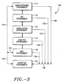
- FIG. 3 shows an SPCIF (SPC integrated fab) 100.
- SPCIF SPC integrated fab
- an SPCIF includes a wafer fab, a wafer fab sub-system or combination of two or more wafer fabs wherein SPC is integrated with one or more wafer fab process control techniques and optionally to other wafer fab systems, sub-systems or components.
- SPCIF 100 shown in FIG. 3, includes a manufacturing environment 110, an SPC environment 112, a computation environment 114, an analysis environment 116, an MES environment 118 and a reporting environment 120.
- Manufacturing environment 110 includes manufacturing apparatus, techniques and methods to manufacture wafer fab devices or device components such as IC structures.
- IC structures as defined herein, includes completely formed ICs and partially formed ICs.
- the manufacturing environment includes such controllers and inputs as are necessary to form the IC structure.
- Suitable controllers include processors for example micro processors such as on-board computers, computer operated software and mechanical/electrical controllers such as switches and electrical circuits employing for example a variable resistor such as a potentiometer. These controllers operate or control various processes and operational functions, such as gas flow rate and wafer handling within manufacturing environment 110.
- Suitable examples of manufacturing environments such as 110 include a wafer fab tool, such as a chamber, or one or more wafer fabs.
- SPCIF 100 schematically illustrated in FIG. 3 provides SPC which is integrated with manufacturing. This integration results in real time monitoring of process control and/or product quality and provides real time process intervention as soon as certain pre-selected process or product parameters are outside the control limits. It also facilitates more effective scheduling of tool availability, materials inventory and real time knowledge as well as scheduling capability for facilities such as electrical power requirements in the manufacturing process.
- MES process intervention environment 256 can be utilized to provide production run information 344 by means of production run information input device 322.
- Such information can include run identification, date or purpose of the run, e.g. testing, production or re-work.
- Wafer and wafer lot identification 346 in wafer fab chamber manufacturing environment 210 can be provided by means of wafer identification input device 324.
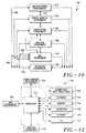
- 12 and 13 is adapted for scheduling the usage of tools in the manufacturing environment such that anticipated power surges occur during relative low power usage periods of the wafer fab.
- pump-down of each of the tools is preferably scheduled such that pump-down is in a planned sequence rather than starting pump-down of several tools simultaneously.
- heating of processing components can be scheduled to avoid simultaneously starting several heaters.
- Manufacturing environment 1110 of wafer fab 1100 includes the processing tools of the wafer fab such as wafer processing chambers and wafer handling tools.
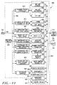
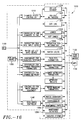
- a wafer processing chamber 1200 suitable for use with the novel spare parts inventory and scheduling system is schematically depicted in FIG. 16. This chamber receives input from MES environment 1150.
- chamber 1200 can receive additional input through non-MES input 1205.
- Inputs from MES environment 1150 and non-MES input 1205 include setting or regulating chamber controllers and providing information to input devices, similar to those described in connection with chamber 800 which is illustrated in FIG. 11. Based on these inputs, chamber controllers and input devices are employed to select the various status, parameter, information and scheduling functions of chamber 1200 similar to those described in connection with chamber 800.
- Spare parts monitor environment 1120 can collect chamber information regarding its status, spare parts and maintenance scheduling, as well as run and wafer ID information. Optionally, this information is displayed or printed, for example by means of reporting environment 1160 as depicted in FIG. 15.
- status information is provided to spare parts monitor environment 1120 by on-line standby 1226, on-line in process 1228, off-line 1230, linked 1232 and not linked 1234.
- Production run 1244 and optionally wafer ID 1246 information are transmitted to spare parts monitor environment 1120.
- Spare parts, also referred to as maintenance parts, schedule 1254 and maintenance activities schedule 1256 are communicated to spare parts monitor environment 1120, see FIG. 16.
- FIG. 19 An additional embodiment of the present invention, schematically illustrated in FIG. 19, shows a wafer fab 1300 including a wafer fab efficiency system.
- This wafer fab efficiency system is integrated with the wafer fab.
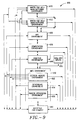
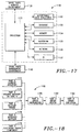
- Wafer fab 1300 includes a manufacturing environment 1310, a scheduling monitor environment 1320, a computation environment 1330, a scheduling management environment 1340, an MES environment 1350 and a reporting environment 1360.
- the novel wafer fab efficiency system comprises: scheduling monitor environment 1320, computation environment 1330 and scheduling management environment 1340.
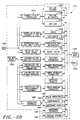
- the various status, parameter, information, metrology and scheduling conditions or results concerning chamber 1400 can be transmitted directly to MES environment 1350, see FIGS. 19 and 20, to provide MES environment 1350 with comprehensive real time information regarding the chamber's status and processing conditions. This information can also be provided on a real time basis to reporting environment 1360 depicted in FIG. 19.
- MES environment 1350, FIG. 19 provide scheduling monitor environment 1320 with a personnel schedule for operating the wafer fab, including for example the manufacturing group, the maintenance group, wafer fab management as well as support personnel. This information can be conveyed to scheduling monitor environment 1320 using for example link 1301 shown in FIG.19.
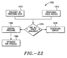
- Algorithm 1335 of the present invention is utilized to optimize the wafer fab process for improved asset utilization.
- This algorithm includes steps 1372 - 1382, as illustrated in FIG. 22.
- step 1372 the sequence of all processing steps for executing the wafer fab process is entered.
- This sequence can for example be obtained from a wafer fab design which has not yet been used in actual production, from a test run, or from a prior production run for this wafer fab.
- the sequence information is generally obtained from MES environment 1350.
- the sequence information resulting from a previous production run can be obtained from database 1333, see FIG. 21.
Landscapes
- Engineering & Computer Science (AREA)
- General Engineering & Computer Science (AREA)
- Manufacturing & Machinery (AREA)
- Quality & Reliability (AREA)
- Physics & Mathematics (AREA)
- General Physics & Mathematics (AREA)
- Automation & Control Theory (AREA)
- General Factory Administration (AREA)
- Testing Or Measuring Of Semiconductors Or The Like (AREA)
- Physical Vapour Deposition (AREA)
- Management, Administration, Business Operations System, And Electronic Commerce (AREA)
Applications Claiming Priority (2)
| Application Number | Priority Date | Filing Date | Title |
|---|---|---|---|
| US323586 | 1999-06-01 | ||
| US09/323,586 US6408220B1 (en) | 1999-06-01 | 1999-06-01 | Semiconductor processing techniques |
Publications (2)
| Publication Number | Publication Date |
|---|---|
| EP1058174A2 true EP1058174A2 (de) | 2000-12-06 |
| EP1058174A3 EP1058174A3 (de) | 2004-06-30 |
Family
ID=23259844
Family Applications (1)
| Application Number | Title | Priority Date | Filing Date |
|---|---|---|---|
| EP00111260A Withdrawn EP1058174A3 (de) | 1999-06-01 | 2000-05-25 | Verfahren zur Bearbeitung von Halbleitern |
Country Status (5)
| Country | Link |
|---|---|
| US (1) | US6408220B1 (de) |
| EP (1) | EP1058174A3 (de) |
| JP (1) | JP2001143980A (de) |
| KR (1) | KR100706584B1 (de) |
| TW (1) | TW452837B (de) |
Cited By (5)
| Publication number | Priority date | Publication date | Assignee | Title |
|---|---|---|---|---|
| US6428673B1 (en) | 2000-07-08 | 2002-08-06 | Semitool, Inc. | Apparatus and method for electrochemical processing of a microelectronic workpiece, capable of modifying processing based on metrology |
| CN101458515B (zh) * | 2007-12-13 | 2011-10-05 | 中芯国际集成电路制造(上海)有限公司 | 晶圆质量分析方法 |
| WO2013023691A1 (de) * | 2011-08-17 | 2013-02-21 | Siemens Aktiengesellschaft | Energiemanagement bei betriebszustandsänderungen einer automatisierungsanlage |
| CN108200778A (zh) * | 2015-11-06 | 2018-06-22 | 株式会社斯库林集团 | 基板处理装置的排程制作方法以及排程制作程序 |
| CN117230417A (zh) * | 2023-08-17 | 2023-12-15 | 沈阳广泰真空科技股份有限公司 | 磁控溅射旋转靶真空镀膜机控制系统及方法 |
Families Citing this family (45)
| Publication number | Priority date | Publication date | Assignee | Title |
|---|---|---|---|---|
| US6678572B1 (en) | 1998-12-31 | 2004-01-13 | Asml Holdings, N.V. | Recipe cascading in a wafer processing system |
| US6865437B1 (en) * | 1998-12-31 | 2005-03-08 | Asml Holdings N.V. | Robot pre-positioning in a wafer processing system |
| US6768930B2 (en) | 1998-12-31 | 2004-07-27 | Asml Holding N.V. | Method and apparatus for resolving conflicts in a substrate processing system |
| US6418356B1 (en) | 1998-12-31 | 2002-07-09 | Silicon Valley Group, Inc. | Method and apparatus for resolving conflicts in a substrate processing system |
| US6763130B1 (en) * | 1999-07-21 | 2004-07-13 | Applied Materials, Inc. | Real time defect source identification |
| AU2001282879A1 (en) | 2000-07-08 | 2002-01-21 | Semitool, Inc. | Methods and apparatus for processing microelectronic workpieces using metrology |
| US6782343B2 (en) * | 2001-02-28 | 2004-08-24 | Asm International N.V. | Resource consumption calculator |
| JP2003077782A (ja) * | 2001-08-31 | 2003-03-14 | Toshiba Corp | 半導体装置の製造方法 |
| US7280883B2 (en) * | 2001-09-06 | 2007-10-09 | Dainippon Screen Mfg. Co., Ltd. | Substrate processing system managing apparatus information of substrate processing apparatus |
| WO2003025685A1 (en) * | 2001-09-14 | 2003-03-27 | Ibex Process Technology, Inc. | Scalable, hierarchical control for complex processes |
| AU2002341677A1 (en) * | 2001-09-18 | 2003-04-01 | Applied Materials, Inc. | Integrated equipment set for forming an interconnect on a substrate |
| US6756243B2 (en) * | 2001-10-30 | 2004-06-29 | Advanced Micro Devices, Inc. | Method and apparatus for cascade control using integrated metrology |
| US20030220708A1 (en) * | 2001-11-28 | 2003-11-27 | Applied Materials, Inc. | Integrated equipment set for forming shallow trench isolation regions |
| US6645780B1 (en) * | 2001-12-13 | 2003-11-11 | Advanced Micro Devices, Inc. | Method and apparatus for combining integrated and offline metrology for process control |
| US6976033B2 (en) * | 2002-04-10 | 2005-12-13 | Charming Systems Corpration | Production cell information system based on activity costs and an architecture therefor |
| TWI266249B (en) * | 2002-05-16 | 2006-11-11 | Mosel Vitelic Inc | Statistical process control method and system thereof |
| US20030225474A1 (en) * | 2002-05-31 | 2003-12-04 | Gustavo Mata | Specialization of active software agents in an automated manufacturing environment |
| US20040007325A1 (en) * | 2002-06-11 | 2004-01-15 | Applied Materials, Inc. | Integrated equipment set for forming a low K dielectric interconnect on a substrate |
| US20040206621A1 (en) * | 2002-06-11 | 2004-10-21 | Hongwen Li | Integrated equipment set for forming a low K dielectric interconnect on a substrate |
| US6773931B2 (en) * | 2002-07-29 | 2004-08-10 | Advanced Micro Devices, Inc. | Dynamic targeting for a process control system |
| US7117057B1 (en) * | 2002-09-10 | 2006-10-03 | Taiwan Semiconductor Manufacturing Co. Ltd. | Yield patrolling system |
| US6650958B1 (en) * | 2002-10-30 | 2003-11-18 | Lsi Logic Corporation | Integrated process tool monitoring system for semiconductor fabrication |
| US6823231B1 (en) * | 2002-11-25 | 2004-11-23 | Advanced Micro Devices, Inc. | Tuning of a process control based upon layer dependencies |
| JP2004206702A (ja) * | 2002-12-12 | 2004-07-22 | Tokyo Electron Ltd | パーツ管理システム及び方法、並びにプログラム及び記憶媒体 |
| US6907369B1 (en) * | 2003-05-02 | 2005-06-14 | Advanced Micro Devices, Inc. | Method and apparatus for modifying design constraints based on observed performance |
| US6947801B2 (en) * | 2003-08-13 | 2005-09-20 | Taiwan Semiconductor Manufacturing Co., Ltd. | Method and system for synchronizing control limit and equipment performance |
| US7187988B2 (en) * | 2003-09-12 | 2007-03-06 | Taiwan Semiconductor Manufacturing Company, Ltd. | Web service and method for customers to define their own alert for real-time production status |
| US7078711B2 (en) * | 2004-02-13 | 2006-07-18 | Applied Materials, Inc. | Matching dose and energy of multiple ion implanters |
| US7035705B2 (en) * | 2004-03-03 | 2006-04-25 | Taiwan Semiconductor Manufacturing Company, Ltd. | System and method for process contamination prevention for semiconductor manufacturing |
| US7120511B1 (en) * | 2004-08-11 | 2006-10-10 | Advanced Micro Devices, Inc. | Method and system for scheduling maintenance procedures based upon workload distribution |
| US20080275582A1 (en) * | 2004-11-19 | 2008-11-06 | Nettles Steven C | Scheduling AMHS pickup and delivery ahead of schedule |
| US20060107898A1 (en) * | 2004-11-19 | 2006-05-25 | Blomberg Tom E | Method and apparatus for measuring consumption of reactants |
| JP2006302952A (ja) * | 2005-04-15 | 2006-11-02 | Toshiba Corp | パターン計測システムおよび半導体装置の製造方法 |
| US20070177788A1 (en) * | 2006-01-31 | 2007-08-02 | David Liu | System and method for detecting wafer failure in wet bench applications |
| US8055370B1 (en) * | 2006-06-23 | 2011-11-08 | Novellus Systems, Inc. | Apparatus and methods for monitoring health of semiconductor process systems |
| US7720553B2 (en) * | 2006-08-31 | 2010-05-18 | Dell Products L.P. | Service metric portfolio management |
| US20080216077A1 (en) * | 2007-03-02 | 2008-09-04 | Applied Materials, Inc. | Software sequencer for integrated substrate processing system |
| JP2009123793A (ja) * | 2007-11-13 | 2009-06-04 | Shimadzu Corp | クラスタ型真空処理装置 |
| GB0800227D0 (en) * | 2008-01-07 | 2008-02-13 | Metryx Ltd | Method of controlling semiconductor device fabrication |
| US9387428B2 (en) * | 2008-02-05 | 2016-07-12 | Applied Materials, Inc. | Systems and methods for treating flammable effluent gases from manufacturing processes |
| KR101555469B1 (ko) * | 2008-02-05 | 2015-09-24 | 어플라이드 머티어리얼스, 인코포레이티드 | 전자 디바이스 제조 시스템을 동작하기 위한 방법 및 장치 |
| JP2010056367A (ja) * | 2008-08-29 | 2010-03-11 | Panasonic Corp | 半導体製造装置 |
| US8151814B2 (en) * | 2009-01-13 | 2012-04-10 | Asm Japan K.K. | Method for controlling flow and concentration of liquid precursor |
| US8938314B2 (en) * | 2010-11-16 | 2015-01-20 | International Business Machines Corporation | Smart energy consumption management |
| WO2025163988A1 (ja) * | 2024-01-31 | 2025-08-07 | 株式会社アルバック | 製造支援装置、製造支援方法、及びプログラム |
Citations (3)
| Publication number | Priority date | Publication date | Assignee | Title |
|---|---|---|---|---|
| US4320463A (en) * | 1980-02-25 | 1982-03-16 | S. Himmelstein And Company | Production control system |
| US5442562A (en) * | 1993-12-10 | 1995-08-15 | Eastman Kodak Company | Method of controlling a manufacturing process using multivariate analysis |
| US5698455A (en) * | 1995-02-09 | 1997-12-16 | Micron Technologies, Inc. | Method for predicting process characteristics of polyurethane pads |
Family Cites Families (45)
| Publication number | Priority date | Publication date | Assignee | Title |
|---|---|---|---|---|
| US5260868A (en) | 1986-08-11 | 1993-11-09 | Texas Instruments Incorporate | Method for calendaring future events in real-time |
| US4890239A (en) | 1987-10-20 | 1989-12-26 | Shipley Company, Inc. | Lithographic process analysis and control system |
| JPH01283934A (ja) | 1988-05-11 | 1989-11-15 | Tokyo Electron Ltd | エッチング装置およびその制御方法 |
| US5108570A (en) | 1990-03-30 | 1992-04-28 | Applied Materials, Inc. | Multistep sputtering process for forming aluminum layer over stepped semiconductor wafer |
| US5236868A (en) | 1990-04-20 | 1993-08-17 | Applied Materials, Inc. | Formation of titanium nitride on semiconductor wafer by reaction of titanium with nitrogen-bearing gas in an integrated processing system |
| AU9030391A (en) | 1990-10-16 | 1992-05-20 | Consilium, Inc. | Object-oriented architecture for factory floor management |
| US5295242A (en) | 1990-11-02 | 1994-03-15 | Consilium, Inc. | Apparatus and method for viewing relationships in a factory management system |
| US5270222A (en) | 1990-12-31 | 1993-12-14 | Texas Instruments Incorporated | Method and apparatus for semiconductor device fabrication diagnosis and prognosis |
| US5257206A (en) * | 1991-04-08 | 1993-10-26 | Praxair Technology, Inc. | Statistical process control for air separation process |
| JP3154425B2 (ja) | 1992-01-07 | 2001-04-09 | フクダ電子株式会社 | 心電図情報記録方法及び装置 |
| US5586041A (en) * | 1992-12-14 | 1996-12-17 | Ford Motor Company | Method and system for real-time statistical process monitoring |
| GB9309513D0 (en) | 1993-05-08 | 1993-06-23 | Univ Coventry | Electrochemical method of modifying biomolecules in particular proteins |
| US5367624A (en) | 1993-06-11 | 1994-11-22 | Consilium, Inc. | Interface for controlling transactions in a manufacturing execution system |
| JPH07141005A (ja) * | 1993-06-21 | 1995-06-02 | Hitachi Ltd | 半導体集積回路装置の製造方法および製造装置 |
| US5408405A (en) | 1993-09-20 | 1995-04-18 | Texas Instruments Incorporated | Multi-variable statistical process controller for discrete manufacturing |
| KR950034499A (ko) | 1994-01-28 | 1995-12-28 | 제임스 조셉 드롱 | 물리적인 증기증착 과정동안 필름들의 증착속도를 모니터하기 위한 방법 및 장치 |
| US5444632A (en) | 1994-04-28 | 1995-08-22 | Texas Instruments Incorporated | Apparatus and method for controlling and scheduling processing machines |
| US5787000A (en) | 1994-05-27 | 1998-07-28 | Lilly Software Associates, Inc. | Method and apparatus for scheduling work orders in a manufacturing process |
| US5629216A (en) | 1994-06-30 | 1997-05-13 | Seh America, Inc. | Method for producing semiconductor wafers with low light scattering anomalies |
| EP0706209A3 (de) | 1994-10-06 | 1996-12-27 | Applied Materials Inc | Flächenwiderstandsmessung |
| JPH08149583A (ja) | 1994-11-21 | 1996-06-07 | Mitsubishi Electric Corp | プロセスコントローラ及びデータ監視方法 |
| JP3315844B2 (ja) | 1994-12-09 | 2002-08-19 | 株式会社東芝 | スケジューリング装置及びスケジューリング方法 |
| KR100213603B1 (ko) | 1994-12-28 | 1999-08-02 | 가나이 쯔또무 | 전자회로기판의 배선수정방법 및 그 장치와 전자회로기판 |
| US5646870A (en) * | 1995-02-13 | 1997-07-08 | Advanced Micro Devices, Inc. | Method for setting and adjusting process parameters to maintain acceptable critical dimensions across each die of mass-produced semiconductor wafers |
| US5715181A (en) | 1995-04-03 | 1998-02-03 | Horst; Robert L. | Isogrammetric analysis method for high-yield processes |
| US5956251A (en) * | 1995-06-28 | 1999-09-21 | The Boeing Company | Statistical tolerancing |
| US5740429A (en) | 1995-07-07 | 1998-04-14 | Advanced Micro Devices, Inc. | E10 reporting tool |
| JPH0934535A (ja) | 1995-07-13 | 1997-02-07 | Mitsubishi Electric Corp | メンテナンス通告方式 |
| US6249712B1 (en) * | 1995-09-26 | 2001-06-19 | William J. N-O. Boiquaye | Adaptive control process and system |
| US5761064A (en) * | 1995-10-06 | 1998-06-02 | Advanced Micro Devices, Inc. | Defect management system for productivity and yield improvement |
| US5719796A (en) * | 1995-12-04 | 1998-02-17 | Advanced Micro Devices, Inc. | System for monitoring and analyzing manufacturing processes using statistical simulation with single step feedback |
| US5864483A (en) * | 1996-08-01 | 1999-01-26 | Electronic Data Systems Corporation | Monitoring of service delivery or product manufacturing |
| US6152070A (en) * | 1996-11-18 | 2000-11-28 | Applied Materials, Inc. | Tandem process chamber |
| US5808303A (en) | 1997-01-29 | 1998-09-15 | Art Aerospace Research Technologies Inc. | Infrared screening and inspection system |
| US5862054A (en) * | 1997-02-20 | 1999-01-19 | Taiwan Semiconductor Manufacturing Company, Ltd. | Process monitoring system for real time statistical process control |
| JP3393035B2 (ja) | 1997-05-06 | 2003-04-07 | 東京エレクトロン株式会社 | 制御装置及び半導体製造装置 |
| US5910011A (en) | 1997-05-12 | 1999-06-08 | Applied Materials, Inc. | Method and apparatus for monitoring processes using multiple parameters of a semiconductor wafer processing system |
| US6201999B1 (en) | 1997-06-09 | 2001-03-13 | Applied Materials, Inc. | Method and apparatus for automatically generating schedules for wafer processing within a multichamber semiconductor wafer processing tool |
| JPH1167853A (ja) | 1997-08-26 | 1999-03-09 | Mitsubishi Electric Corp | ウェーハマップ解析補助システムおよびウェーハマップ解析方法 |
| US6128588A (en) | 1997-10-01 | 2000-10-03 | Sony Corporation | Integrated wafer fab time standard (machine tact) database |
| KR100278600B1 (ko) | 1998-01-14 | 2001-01-15 | 윤종용 | 반도체 제조설비 관리시스템의 설비유닛의 상태 관리방법 |
| US6054379A (en) | 1998-02-11 | 2000-04-25 | Applied Materials, Inc. | Method of depositing a low k dielectric with organo silane |
| US6223091B1 (en) * | 1998-05-29 | 2001-04-24 | Siemens Energy & Automation, Inc. | Alarm event generator apparatus, means and system |
| US6138143A (en) * | 1999-01-28 | 2000-10-24 | Genrad, Inc. | Method and apparatus for asynchronous transaction processing |
| US6303395B1 (en) | 1999-06-01 | 2001-10-16 | Applied Materials, Inc. | Semiconductor processing techniques |
-
1999
- 1999-06-01 US US09/323,586 patent/US6408220B1/en not_active Expired - Fee Related
-
2000
- 2000-05-25 EP EP00111260A patent/EP1058174A3/de not_active Withdrawn
- 2000-05-29 TW TW089110420A patent/TW452837B/zh not_active IP Right Cessation
- 2000-06-01 KR KR1020000030182A patent/KR100706584B1/ko not_active Expired - Fee Related
- 2000-06-01 JP JP2000164624A patent/JP2001143980A/ja active Pending
Patent Citations (3)
| Publication number | Priority date | Publication date | Assignee | Title |
|---|---|---|---|---|
| US4320463A (en) * | 1980-02-25 | 1982-03-16 | S. Himmelstein And Company | Production control system |
| US5442562A (en) * | 1993-12-10 | 1995-08-15 | Eastman Kodak Company | Method of controlling a manufacturing process using multivariate analysis |
| US5698455A (en) * | 1995-02-09 | 1997-12-16 | Micron Technologies, Inc. | Method for predicting process characteristics of polyurethane pads |
Cited By (5)
| Publication number | Priority date | Publication date | Assignee | Title |
|---|---|---|---|---|
| US6428673B1 (en) | 2000-07-08 | 2002-08-06 | Semitool, Inc. | Apparatus and method for electrochemical processing of a microelectronic workpiece, capable of modifying processing based on metrology |
| CN101458515B (zh) * | 2007-12-13 | 2011-10-05 | 中芯国际集成电路制造(上海)有限公司 | 晶圆质量分析方法 |
| WO2013023691A1 (de) * | 2011-08-17 | 2013-02-21 | Siemens Aktiengesellschaft | Energiemanagement bei betriebszustandsänderungen einer automatisierungsanlage |
| CN108200778A (zh) * | 2015-11-06 | 2018-06-22 | 株式会社斯库林集团 | 基板处理装置的排程制作方法以及排程制作程序 |
| CN117230417A (zh) * | 2023-08-17 | 2023-12-15 | 沈阳广泰真空科技股份有限公司 | 磁控溅射旋转靶真空镀膜机控制系统及方法 |
Also Published As
| Publication number | Publication date |
|---|---|
| EP1058174A3 (de) | 2004-06-30 |
| KR20010029773A (ko) | 2001-04-16 |
| TW452837B (en) | 2001-09-01 |
| KR100706584B1 (ko) | 2007-04-11 |
| JP2001143980A (ja) | 2001-05-25 |
| US6408220B1 (en) | 2002-06-18 |
Similar Documents
| Publication | Publication Date | Title |
|---|---|---|
| EP1058175B1 (de) | Verfahren zur Bearbeitung von Halbleitern | |
| US6408220B1 (en) | Semiconductor processing techniques | |
| US6456894B1 (en) | Semiconductor processing techniques | |
| US6556949B1 (en) | Semiconductor processing techniques | |
| US7454317B2 (en) | Apparatus productivity improving system and its method | |
| KR100566192B1 (ko) | 반도체 제조 장치의 원격 보수 시스템, 반도체 제조 장치의 원격 보수 시스템의 공장측 클라이언트, 반도체 제조 장치의 원격 보수 시스템의 벤더측 서버, 원격 보수 방법, 및 컴퓨터 프로그램이 저장된 기억 매체 | |
| US20040158474A1 (en) | Service facility for providing remote diagnostic and maintenance services to a process plant | |
| US6790686B1 (en) | Method and apparatus for integrating dispatch and process control actions | |
| KR20040015813A (ko) | 런투런 제어와 고장 검출의 통합 | |
| JP2000252179A (ja) | 半導体製造プロセス安定化支援システム | |
| GB2347233A (en) | Diagnostics in a process control system which uses multi-variable control techniques | |
| EP1058173A2 (de) | Verfahren zur Bearbeitung von Halbleitern | |
| US6732007B1 (en) | Method and apparatus for implementing dynamic qualification recipes | |
| CN120124312B (zh) | 一种自适应的半导体设备用能数字孪生仿真装置及方法 | |
| Bouaziz et al. | Dependability of complex semiconductor systems: Learning Bayesian networks for decision support | |
| CN121596783A (zh) | 智能监控方法、系统及半导体生产系统 | |
| BOUAZIZ et al. | Dependability of complex semiconductor systems |
Legal Events
| Date | Code | Title | Description |
|---|---|---|---|
| PUAI | Public reference made under article 153(3) epc to a published international application that has entered the european phase |
Free format text: ORIGINAL CODE: 0009012 |
|
| AK | Designated contracting states |
Kind code of ref document: A2 Designated state(s): AT BE CH CY DE DK ES FI FR GB GR IE IT LI LU MC NL PT SE |
|
| AX | Request for extension of the european patent |
Free format text: AL;LT;LV;MK;RO;SI |
|
| PUAL | Search report despatched |
Free format text: ORIGINAL CODE: 0009013 |
|
| AK | Designated contracting states |
Kind code of ref document: A3 Designated state(s): AT BE CH CY DE DK ES FI FR GB GR IE IT LI LU MC NL PT SE |
|
| AX | Request for extension of the european patent |
Extension state: AL LT LV MK RO SI |
|
| 17P | Request for examination filed |
Effective date: 20041202 |
|
| AKX | Designation fees paid |
Designated state(s): DE GB |
|
| 17Q | First examination report despatched |
Effective date: 20050225 |
|
| STAA | Information on the status of an ep patent application or granted ep patent |
Free format text: STATUS: THE APPLICATION IS DEEMED TO BE WITHDRAWN |
|
| 18D | Application deemed to be withdrawn |
Effective date: 20060309 |