EP1058231A2 - Dünnfilmtransistor-Flüssigkristall-Anzeige mit gemeinsamer Mehrphasenladungsbenutzung und Steuerverfahren dafür - Google Patents
Dünnfilmtransistor-Flüssigkristall-Anzeige mit gemeinsamer Mehrphasenladungsbenutzung und Steuerverfahren dafür Download PDFInfo
- Publication number
- EP1058231A2 EP1058231A2 EP00111643A EP00111643A EP1058231A2 EP 1058231 A2 EP1058231 A2 EP 1058231A2 EP 00111643 A EP00111643 A EP 00111643A EP 00111643 A EP00111643 A EP 00111643A EP 1058231 A2 EP1058231 A2 EP 1058231A2
- Authority
- EP
- European Patent Office
- Prior art keywords
- voltage
- charge sharing
- tft
- lcd
- source
- Prior art date
- Legal status (The legal status is an assumption and is not a legal conclusion. Google has not performed a legal analysis and makes no representation as to the accuracy of the status listed.)
- Granted
Links
Images


Classifications
-
- G—PHYSICS
- G02—OPTICS
- G02F—OPTICAL DEVICES OR ARRANGEMENTS FOR THE CONTROL OF LIGHT BY MODIFICATION OF THE OPTICAL PROPERTIES OF THE MEDIA OF THE ELEMENTS INVOLVED THEREIN; NON-LINEAR OPTICS; FREQUENCY-CHANGING OF LIGHT; OPTICAL LOGIC ELEMENTS; OPTICAL ANALOGUE/DIGITAL CONVERTERS
- G02F1/00—Devices or arrangements for the control of the intensity, colour, phase, polarisation or direction of light arriving from an independent light source, e.g. switching, gating or modulating; Non-linear optics
- G02F1/01—Devices or arrangements for the control of the intensity, colour, phase, polarisation or direction of light arriving from an independent light source, e.g. switching, gating or modulating; Non-linear optics for the control of the intensity, phase, polarisation or colour
- G02F1/13—Devices or arrangements for the control of the intensity, colour, phase, polarisation or direction of light arriving from an independent light source, e.g. switching, gating or modulating; Non-linear optics for the control of the intensity, phase, polarisation or colour based on liquid crystals, e.g. single liquid crystal display cells
- G02F1/133—Constructional arrangements; Operation of liquid crystal cells; Circuit arrangements
-
- G—PHYSICS
- G09—EDUCATION; CRYPTOGRAPHY; DISPLAY; ADVERTISING; SEALS
- G09G—ARRANGEMENTS OR CIRCUITS FOR CONTROL OF INDICATING DEVICES USING STATIC MEANS TO PRESENT VARIABLE INFORMATION
- G09G3/00—Control arrangements or circuits, of interest only in connection with visual indicators other than cathode-ray tubes
- G09G3/20—Control arrangements or circuits, of interest only in connection with visual indicators other than cathode-ray tubes for presentation of an assembly of a number of characters, e.g. a page, by composing the assembly by combination of individual elements arranged in a matrix no fixed position being assigned to or needed to be assigned to the individual characters or partial characters
- G09G3/34—Control arrangements or circuits, of interest only in connection with visual indicators other than cathode-ray tubes for presentation of an assembly of a number of characters, e.g. a page, by composing the assembly by combination of individual elements arranged in a matrix no fixed position being assigned to or needed to be assigned to the individual characters or partial characters by control of light from an independent source
- G09G3/36—Control arrangements or circuits, of interest only in connection with visual indicators other than cathode-ray tubes for presentation of an assembly of a number of characters, e.g. a page, by composing the assembly by combination of individual elements arranged in a matrix no fixed position being assigned to or needed to be assigned to the individual characters or partial characters by control of light from an independent source using liquid crystals
- G09G3/3611—Control of matrices with row and column drivers
- G09G3/3614—Control of polarity reversal in general
-
- G—PHYSICS
- G09—EDUCATION; CRYPTOGRAPHY; DISPLAY; ADVERTISING; SEALS
- G09G—ARRANGEMENTS OR CIRCUITS FOR CONTROL OF INDICATING DEVICES USING STATIC MEANS TO PRESENT VARIABLE INFORMATION
- G09G3/00—Control arrangements or circuits, of interest only in connection with visual indicators other than cathode-ray tubes
- G09G3/20—Control arrangements or circuits, of interest only in connection with visual indicators other than cathode-ray tubes for presentation of an assembly of a number of characters, e.g. a page, by composing the assembly by combination of individual elements arranged in a matrix no fixed position being assigned to or needed to be assigned to the individual characters or partial characters
- G09G3/34—Control arrangements or circuits, of interest only in connection with visual indicators other than cathode-ray tubes for presentation of an assembly of a number of characters, e.g. a page, by composing the assembly by combination of individual elements arranged in a matrix no fixed position being assigned to or needed to be assigned to the individual characters or partial characters by control of light from an independent source
- G09G3/36—Control arrangements or circuits, of interest only in connection with visual indicators other than cathode-ray tubes for presentation of an assembly of a number of characters, e.g. a page, by composing the assembly by combination of individual elements arranged in a matrix no fixed position being assigned to or needed to be assigned to the individual characters or partial characters by control of light from an independent source using liquid crystals
- G09G3/3611—Control of matrices with row and column drivers
- G09G3/3685—Details of drivers for data electrodes
- G09G3/3688—Details of drivers for data electrodes suitable for active matrices only
-
- G—PHYSICS
- G09—EDUCATION; CRYPTOGRAPHY; DISPLAY; ADVERTISING; SEALS
- G09G—ARRANGEMENTS OR CIRCUITS FOR CONTROL OF INDICATING DEVICES USING STATIC MEANS TO PRESENT VARIABLE INFORMATION
- G09G2310/00—Command of the display device
- G09G2310/02—Addressing, scanning or driving the display screen or processing steps related thereto
- G09G2310/0243—Details of the generation of driving signals
- G09G2310/0248—Precharge or discharge of column electrodes before or after applying exact column voltages
-
- G—PHYSICS
- G09—EDUCATION; CRYPTOGRAPHY; DISPLAY; ADVERTISING; SEALS
- G09G—ARRANGEMENTS OR CIRCUITS FOR CONTROL OF INDICATING DEVICES USING STATIC MEANS TO PRESENT VARIABLE INFORMATION
- G09G2330/00—Aspects of power supply; Aspects of display protection and defect management
- G09G2330/02—Details of power systems and of start or stop of display operation
- G09G2330/021—Power management, e.g. power saving
- G09G2330/023—Power management, e.g. power saving using energy recovery or conservation
-
- G—PHYSICS
- G09—EDUCATION; CRYPTOGRAPHY; DISPLAY; ADVERTISING; SEALS
- G09G—ARRANGEMENTS OR CIRCUITS FOR CONTROL OF INDICATING DEVICES USING STATIC MEANS TO PRESENT VARIABLE INFORMATION
- G09G3/00—Control arrangements or circuits, of interest only in connection with visual indicators other than cathode-ray tubes
- G09G3/20—Control arrangements or circuits, of interest only in connection with visual indicators other than cathode-ray tubes for presentation of an assembly of a number of characters, e.g. a page, by composing the assembly by combination of individual elements arranged in a matrix no fixed position being assigned to or needed to be assigned to the individual characters or partial characters
- G09G3/2007—Display of intermediate tones
- G09G3/2011—Display of intermediate tones by amplitude modulation
Definitions
- the present invention relates to a thin film transistor-liquid crystal display (TFT-LCD) and, more particularly, to a TFT-LCD using multi-phase charge sharing and a method for driving the same, in which source lines of the liquid crystal panel are driven with a low power through charge sharing, to reduce the consumption power of a TFT-LCD driving circuit.
- TFT-LCD thin film transistor-liquid crystal display
- a TFT-LCD is being widely used as a screen for a desk-top computer, TV, computer's monitor because it has the most excellent properties in a variety of LCDs, such as high image quality similar to that of CRT, high-speed response and so on.
- a conventional TFT-LCD as shown in FIG. 1, includes a liquid crystal panel 10 having a plurality of pixels each of which is located at the point where each of a plurality of gate lines GL intersects each of a plurality of source lines SL, a source driver 20 for supplying a video signal to each of the pixels through a corresponding source line SL of the liquid crystal panel 10, and a gate driver 30 for selecting a gate line GL of the liquid crystal panel 10 to turn on plural pixels.
- Each pixel consists of a thin film transistor 1 whose gate is connected to a corresponding gate line GL and whose drain is connected to a corresponding source line SL, and a storage capacitor Cs and a liquid crystal capacitor CIc which are connected to the source of the thin film transistor 1 in parallel.
- a sampling register (not shown) of the source driver 20 sequentially receives video data items each of which corresponds to one pixel and stores them which correspond to the source lines SL, respectively.
- the video data items which are stored in the sampling register are transferred to the holding register by the signal of the controller.
- the gate driver 30 outputs a gate line selection signal GLS, to select a gate line GL among the plural gate lines GL. Accordingly, the plural thin film transistors connected to the selected gate line GL are turned on to allow the video data stored in the holding register of the source driver 20 to be applied to their drains, thereby displaying the video data on the liquid crystal panel 10.
- the source driver 20 supplies VCOM, a positive video signal and a negative video signal to the liquid crystal panel 10, to thereby display the video data thereon. That is, in the operation of the convention TFT-LCD, as shown in FIG. 2, the positive video signal and the negative video signal are alternately supplied to the pixels whenever a frame changes in order not to directly apply DC voltage to the liquid crystal. For this, the intermediate voltage between the positive and negative video signals, VCOM, is applied to an electrode formed on an upper plate of the TFT-LCD.
- VCOM the intermediate voltage between the positive and negative video signals
- FIGS. 3A to 3D To reduce the generation of flicker, there is employed one of a frame inversion, line inversion, column inversion and dot inversion, shown in FIGS. 3A to 3D, respectively.
- the frame inversion of FIG. 3A is a mode that the polarity of the video signal is changed only when the frame is changed.
- the line inversion of FIG. 3B is a mode that the video signal's polarity is varied whenever the gate line GL changes.
- the column inversion shown in FIG. 3C converts the polarity of the video signal whenever the source line SL changes, and the dot inversion of FIG. 3D converts it whenever the source line SL, gate line GL and frame change.
- the image quality is satisfactory in the order of the frame inversion, line inversion, column inversion and dot inversion. A higher image quality requires higher power consumption because the number of the generation of polarity conversions increases in proportional to the image quality. This is explained below with reference to the dot inversion shown in FIG. 4.
- FIG. 4 illustrates the waveforms of an odd-numbered source line SL and an even-number source line SL, applied to the liquid crystal panel 10, showing that the video signals of the source lines SL change their polarities on the basis of VCOM whenever the gate line GL changes.
- the video signal swing width V of the source lines SL is twice the sum of VCOM and the swing width of the positive video signal or the sum of VCOM and the swing width of the negative video signal.
- the dot inversion consumes a large amount of power because the video signal changes its polarity from (+) to (-) or from (-) to (+) on the basis of VCOM whenever the gate line GL changes.
- the conventional TFT-LCD consumes a larger quantity of power to increase the generation of heat in case where its TFT is configured of a polysilicon TFT. Accordingly, the characteristic of the liquid crystal and the property of the TFT are deteriorated due to the heat generated.
- the source driver supplies both ends of the liquid crystal with a voltage higher than the common electrode voltage in the nth frame, and supplies them with a voltage lower than the common electrode voltage in the (n+1)th frame, the voltages, respectively applied to the pixels placed above the same column line and the pixels placed therebelow, having their polarities different from each other, and the voltages, respectively applied to the pixels placed at the left side of the same row line and the pixels located at the right side thereof, having their polarities different from each other even in the same nth frame.
- This TFT-LCD is driven in such a manner that charge sharing is performed with charge sharing time set for every row line for charge sharing, and then a voltage corresponding to video data is applied to each pixel. Since the voltage polarity of odd-numbered pixels of the (M-1)th low line is different from that of even-numbered pixels thereof, odd-numbered source lines are connected to even-numbered source lines through a switching element before a desired amount of voltage corresponding to the video data is applied to the pixels of the Mth row line. By doing so, the source line to which the voltage higher than the common electrode voltage is applied to and the source line to which the voltage lower than the common electrode voltage is applied maintain the maximum voltage at the common electrode through charge sharing.
- the source driving circuit reduces the voltage swing width by half in comparison with that of the conventional circuit, decreasing the power consumed for driving the TFT-LCD.
- the conventional TFT-LCD using charge sharing connects the odd-numbered source lines SL to the even-numbered source lines SL using a transfer gate for a period of blanking time, to move a part of the charges of the source lines charged with the positive video signal to the source lines charged with the negative video signal to allow them to share the charges. Accordingly, the consumption power is reduced by 50% at most.
- the conventional TFT-LCD requires a plurality of source drivers in order to realize a higher resolution of VGA class ⁇ SVGA class ⁇ XGA class ⁇ SXGA class ⁇ UXGA class. This narrows the line pitch, bring about reliability problems.
- the present invention is directed to a TFT-LCD using multi-phase charge sharing and a method for driving the same that substantially obviates one or more of the problems due to limitations and disadvantages of the related art.
- An object of the present invention is to provide a TFT-LCD using multi-phase charge sharing, which solves reliability problem between the source lines thereof due to addition of source drivers for realizing a high resolution, and reduces power consumption.
- the present invention provides the method for driving the TFT-LCD using multi-phase charge sharing, whose consumption power is reduced much more than that of the conventional TFT-LCD using charge sharing.
- a TFT-LCD using multi-phase charge sharing comprising: a source driver for outputting video data signals each of which corresponds to one pixel through a plurality of source lines; switching elements for multi-phase charge sharing; and an external capacitor, connected between a liquid crystal panel and the source driver, for collecting charges of a source line having a voltage higher than a common electrode voltage and supplying them to a source line having a voltage lower than the common electrode voltage when the source lines are connected thereto.
- a method for driving a TFT-LCD using multi-phase charge sharing in which at least one selection signal is applied to drive the TFT-LCD for a period of multi-phase charge sharing time, the method comprising: a first charge sharing step in which even-numbered capacitors, which have been discharged with a voltage V L during a period of (N-1)th gradation expressing time, are charged with the voltage of an external capacitor, V L +(1/3)Vswing, according to a second selection signal; a second charge sharing step in which odd-numbered capacitors, which have been charged with a voltage V H during the period of the (N-1)th gradation expressing time, are charged with a voltage V L +(2/3)Vswing through charge sharing with the even-numbered capacitors charged with V L +(1/3)Vswing by the first charge sharing, according to a third selection signal; and a third charge sharing step in which the odd-numbered capacitors, which should be discharged with V L during a period
- the TFT-LCD using multi-phase charge sharing includes a line driver 200 which outputs video data signals each of which corresponds to each pixel through a plurality of source lines, a liquid crystal panel 100 for displaying the video signals applied through the source lines, and an external capacitor 500, connected between the line driver 200 and the liquid crystal panel 100, for collecting charges of source lines having a voltage higher than a common electrode voltage and supplying them to source lines having a voltage lower than the common electrode voltage when the source lines are connected thereto.
- the line driver 200 includes a source driver 300 for supplying the pixels with video signals through the source lines of the liquid crystal panel 100, and a switching section 400 for connecting the source lines of the liquid crystal panel 100 to the source driver 300 or the external capacitor 500 according to an external driving signal.
- a source driver 300 for supplying the pixels with video signals through the source lines of the liquid crystal panel 100
- a switching section 400 for connecting the source lines of the liquid crystal panel 100 to the source driver 300 or the external capacitor 500 according to an external driving signal.
- odd-numbered source lines are connected to output terminals of the source driver 300 or the external capacitor 500 according to a first selection signal SEL1.
- even-numbered source lines are connected to output terminals of the source driver 300 or the external capacitor 500 according to a second selection signal SEL2.
- each source line has a capacitive load and a resistive load.
- a capacitance C load represents the source line's capacitor operating as the capacitive load
- a resistance R oad represents the resistive load of the source line.
- the external capacitor C ext has capacitance much larger than the capacitance C load , and it serves as an auxiliary power supply charging the capacitance C load .
- FIG. 6 shows the input/output waveforms of signals of sections constructing the driving circuit of the TFT-LCD according to the present invention, illustrating the selection signals applied to the line switching section 400 and a voltage whose charges are shared according to these selection signals.
- the number of the capacitive loads C load is M
- the number of the capacitive loads charged with a voltage V H is M/2
- the number of the capacitive loads C load discharged with a voltage V L is M/2.
- V H corresponds to a source line voltage having the positive polarity for expressing a multilevel image
- V L corresponds to an odd-numbered source line voltage having the negative polarity for expressing the same multilevel image.
- the odd-numbered capacitive loads C load have been charged with V H and the even-numbered capacitive loads C load have been discharged with V L after a lapse of the driving time of the (N-1)th capacitive loads C load .
- the odd-numbered capacitive loads C load are discharged with V L and the even-numbered capacitive loads C load are charged with V H during a period of the driving time of the Nth capacitive load.
- the external capacitor C ext is considerably larger than the capacitive load C load and charged with a predetermined-level voltage to operate as a voltage source substantially.
- the external capacitor C ext is charged with the voltage of V L +(1/3)Vswing, as explained below, to serve as the voltage source even when the voltage is not externally applied thereto.
- the Vswing represents the difference between V H and V L .
- the Vswing means the voltage swing width supplied by the conventional source driver in order to charge the capacitive load C load having V L with V H .
- the output terminals of the source driver 300 are in a high impedance state during multi-phase charge sharing period. There will be explained below a method for driving the TFT-LCD using multi-phase charge sharing according to the present invention under the aforementioned conditions.
- the line switches to which the second selection signal SEL2 is applied are turned off and line switches with which the third selection signal SEL3 is provided are turned on. Accordingly, the odd-numbered capacitive loads C load which have been charged with V H during the period of the (N-1)th gradation expressing time are connected to the even-numbered capacitive loads C load charged with V L +(1/3)Vswing at the first charge sharing stage, to allow all of the capacitive loads to have a voltage V L +(2/3)Vswing higher than the V L +(1/2)Vswing.
- the line switches to which the third selection signal SEL3 is applied are turned off and line switches with which the first selection signal SEL1 is provided are turned on. Accordingly, the odd-numbered capacitive loads C load which should be discharged with V L during a period of the Nth gradation expressing time are connected to the external capacitor C ext to share charges. At this time, the capacitive loads C load have the voltage of V L +(1/3)Vswing of the external capacitor C ext . After this, the line switches to which the first selection signal SEL1 is applied are turned off, completing the multi-phase charge sharing.
- the odd-numbered capacitive loads C load Upon completion of the Nth multi-phase charge sharing, the odd-numbered capacitive loads C load become the voltage of V L +(1/3)Vswing and the even-numbered capacitive loads C load become the voltage of V L +(2/3)Vswing. Subsequently, the output driver of the liquid crystal panel 100 charges the even-numbered capacitive loads C load having the V L +(2/3)Vswing with V H , and discharges the odd-numbered capacitive loads C load with V L during a period of gradation expressing time.
- FIG. 7 is a block diagram of a TFT-LCD driving circuit according to an embodiment of the present invention
- FIG. 8 is a block diagram of a TFT-LCD driving circuit according to another embodiment of the present invention.
- the TFT-LCD driving circuit according to the present invention is identical to the TFT-LCD driving circuit of FIG. 5 in the basic configuration and has a difference from that in that the line switching section 400 is configured of transfer gates.
- the TFT-LCD driving circuit of this embodiment performs multi-phase charge sharing operation as described above.
- the line switching section 400 may be configured of PMOS transistors or NMOS transistors other than the transfer gates. The detailed configuration of the line switching section will be explained below.
- the line switching section 400 includes a transfer gate part 410 for making the output terminals of the source driver 300 be in the high impedance state according to control signals AMP and AMP_B, first and second switching parts 420 and 430 for connecting each source line of the liquid crystal panel 100 to the external capacitor 500 according to the first and second selection signals SEL1 and SEL2, respectively, and a third switching part 440 connected to the source lines adjacent to the liquid crystal panel 100 according to the third selection signal SEL3.
- the third switching part 440 is configured of transfer gates each of which is connected to each of the source lines adjacent to the liquid crystal panel.
- each of switches constructing the third switching part 440 is connected to the (2N-1)th and 2Nth source lines. That is, each of the transfer gates constructing the third switching part 440 is connected only between the (2N-1)th and 2Nth source lines, but is not connected between the 2Nth and (2N+1)th source lines.
- the consumption power of the TFT-LCD can be obtained using the following formula.
- V DD represents the supply power
- Vswing indicates the width of a voltage charging and discharging the capacitive load
- C L indicates the capacitive load
- freq represents a driving frequency when the capacitive loads are charged or discharged.
- the voltage width Vswing deciding a consumption power index is determined by waveforms shown in FIG. 9. Although the Vswing became (1/2)Vswing after charge sharing in the conventional driving method according to the aforementioned formula, it was confirmed through HSPICE that the Vswing is reduced to (1/3)Vswing maximum through the multi-phase charge sharing in the present invention.
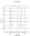
- the voltage swing width for expressing white is the narrowest. This corresponds to "normally white” that light is transmitted through the liquid crystal without application of voltage.
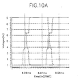
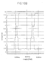
- FIG. 10C shows the waveforms of sharing voltage when a white image is expressed. Furthermore, the voltage swing width of the medium gray is a little wider than that of white, and the voltage swing width in case of black is the widest.
- FIGS. 10A and 10B show the waveforms of sharing voltages when the black and medium gray images are expressed, respectively.
- the voltage of the capacitive load after the multi-phase charge sharing obtains the same characteristic whether it is initially charged or not.
- the voltage width Vswing is reduced to (1/3)Vswing in comparison with the conventional one, reaching a consumption power reduction efficiency of 66.6% under a predetermined simulation condition.
- the consumption power reduction efficiency can be varied with RC time constants of the source lines and the length of charge sharing time of the source lines.
- the external capacitor can be initially charged with the voltage V L +(1/3)Vswing or more, and, even if it is not charged, charged with V L +(1/3)Vswing according to the driving method proposed by the present invention, to substantially operate as a voltage source. Accordingly, it can be confirmed through the HSPICE simulation shown in FIGS. 10A, 10B and 10C that the TFT-LCD of the present invention increases more its consumption power reduction efficiency as the magnitude of the resistive load of the source lines decreases or the charge sharing time thereof increases.
- FIG. 11 shows the voltage waveform of the external capacitance C ext when the black image is expressed according to the driving method of the present invention, being confirmed through the HSPICE simulation.
- the external capacitance is charged while the TFT-LCD is driven even if it has not been initially charged, to operate as a voltage source.
- the voltage of the external capacitance confirmed through the simulation, becomes 3.666V after a lapse of predetermined time. At this time, though the voltage of the external capacitance depends on video signals, there is no variation in the average consumption power reduction efficiency.
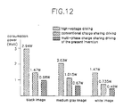
- FIG. 12 is a graph showing the consumption power when an SXGA class TFT-LCD is driven according to the present invention. From this graph, it is observed that the driving consumption power of the present invention is reduced to one-third of the conventional one without regard to video images.
- the circuit driving a TFT-LCD using multi-phase charge sharing has the following advantages.
- the TFT-LCD driving circuit shares the charges of the source lines during the period of multi-phase charge sharing time, to thereby reduce the driving power consumption of the liquid crystal panel to one-third of the conventional one.
- the TFT-LCD driving circuit of the present invention generates less heat due to reduction in its consumption power. Thus, deterioration in characteristics of the liquid crystal and TFT caused by heat is decreased in case where the TFT-LCD is configured of a polysilicon TFT.
- the high-resolution TFT-LCD according to the present invention uses at least one line switching element to solve reliability problem between the source lines due to addition of source drivers, realizing a low-power liquid crystal display.
- the switching section of the source driver can be configured of a variety of switching elements.
Landscapes
- Physics & Mathematics (AREA)
- Engineering & Computer Science (AREA)
- General Physics & Mathematics (AREA)
- Crystallography & Structural Chemistry (AREA)
- Chemical & Material Sciences (AREA)
- Theoretical Computer Science (AREA)
- Computer Hardware Design (AREA)
- Nonlinear Science (AREA)
- Liquid Crystal (AREA)
- Mathematical Physics (AREA)
- Optics & Photonics (AREA)
- Liquid Crystal Display Device Control (AREA)
- Control Of Indicators Other Than Cathode Ray Tubes (AREA)
Applications Claiming Priority (2)
| Application Number | Priority Date | Filing Date | Title |
|---|---|---|---|
| KR9920469 | 1999-06-03 | ||
| KR1019990020469A KR100312344B1 (ko) | 1999-06-03 | 1999-06-03 | 다단계 전하 재활용을 이용한 tft-lcd 및 그 방법 |
Publications (3)
| Publication Number | Publication Date |
|---|---|
| EP1058231A2 true EP1058231A2 (de) | 2000-12-06 |
| EP1058231A3 EP1058231A3 (de) | 2001-02-07 |
| EP1058231B1 EP1058231B1 (de) | 2012-05-09 |
Family
ID=19589809
Family Applications (1)
| Application Number | Title | Priority Date | Filing Date |
|---|---|---|---|
| EP00111643A Expired - Lifetime EP1058231B1 (de) | 1999-06-03 | 2000-05-31 | Dünnfilmtransistor-Flüssigkristall-Anzeige mit gemeinsamer Mehrphasenladungsbenutzung und Steuerverfahren dafür |
Country Status (7)
| Country | Link |
|---|---|
| US (2) | US6549186B1 (de) |
| EP (1) | EP1058231B1 (de) |
| JP (1) | JP3415810B2 (de) |
| KR (1) | KR100312344B1 (de) |
| CN (1) | CN1162827C (de) |
| AT (1) | ATE557383T1 (de) |
| TW (1) | TW525129B (de) |
Cited By (2)
| Publication number | Priority date | Publication date | Assignee | Title |
|---|---|---|---|---|
| EP1414009A1 (de) * | 2002-10-24 | 2004-04-28 | Dialog Semiconductor GmbH | Reduzierung des Energieverbrauches für Flüssigkristall-Anzeigesteuergeräte durch Ladungsverteilung von Rückwandverdrahtungen |
| CN100440301C (zh) * | 2004-03-23 | 2008-12-03 | 株式会社日立显示器 | 液晶显示装置 |
Families Citing this family (62)
| Publication number | Priority date | Publication date | Assignee | Title |
|---|---|---|---|---|
| US7274383B1 (en) * | 2000-07-28 | 2007-09-25 | Clairvoyante, Inc | Arrangement of color pixels for full color imaging devices with simplified addressing |
| JP4702725B2 (ja) * | 2000-08-04 | 2011-06-15 | 財団法人工業技術研究院 | 液晶ディスプレーの駆動方法及び駆動回路 |
| JP2002091387A (ja) * | 2000-09-13 | 2002-03-27 | Kawasaki Microelectronics Kk | Lcdドライバ |
| KR100468614B1 (ko) * | 2000-10-25 | 2005-01-31 | 매그나칩 반도체 유한회사 | 액정 표시 장치를 위한 저전력 컬럼 구동 방법 |
| JP4062876B2 (ja) * | 2000-12-06 | 2008-03-19 | ソニー株式会社 | アクティブマトリクス型表示装置およびこれを用いた携帯端末 |
| KR100759974B1 (ko) * | 2001-02-26 | 2007-09-18 | 삼성전자주식회사 | 액정 표시 장치 및 그의 구동 방법. |
| US7102608B2 (en) * | 2002-06-21 | 2006-09-05 | Himax Technologies, Inc. | Method and related apparatus for driving pixels located in a row of an LCD panel toward the same average voltage value |
| CN1309569C (zh) | 2002-01-28 | 2007-04-11 | 夏普株式会社 | 容性负载驱动电路以及容性负载驱动方法及使用这些的装置 |
| JP3908057B2 (ja) * | 2002-02-26 | 2007-04-25 | Necエレクトロニクス株式会社 | 液晶駆動用半導体集積回路装置 |
| JP3820379B2 (ja) * | 2002-03-13 | 2006-09-13 | 松下電器産業株式会社 | 液晶駆動装置 |
| KR100477975B1 (ko) * | 2002-06-18 | 2005-03-23 | 삼성에스디아이 주식회사 | 유기 전계발광 표시 장치의 구동 회로 및 구동 방법 |
| JP3722812B2 (ja) * | 2003-07-08 | 2005-11-30 | シャープ株式会社 | 容量性負荷の駆動回路および駆動方法 |
| JP5238126B2 (ja) * | 2004-11-24 | 2013-07-17 | 株式会社半導体エネルギー研究所 | 表示装置とその駆動方法 |
| TWI267820B (en) * | 2004-12-07 | 2006-12-01 | Novatek Microelectronics Corp | Source driver and panel displaying device |
| US7663594B2 (en) * | 2005-05-17 | 2010-02-16 | Lg Display Co., Ltd. | Liquid crystal display device with charge sharing function and driving method thereof |
| KR100719083B1 (ko) * | 2005-06-03 | 2007-05-16 | 엘지전자 주식회사 | 액정 표시장치의 구동 장치 및 그 구동 방법 |
| TW200643880A (en) * | 2005-06-07 | 2006-12-16 | Sunplus Technology Co Ltd | LCD panel driving method and device thereof |
| KR100614661B1 (ko) * | 2005-06-07 | 2006-08-22 | 삼성전자주식회사 | 액정 표시 장치의 소스 드라이버 출력 회로 및 데이터 라인구동방법 |
| CN100388351C (zh) * | 2005-06-09 | 2008-05-14 | 凌阳科技股份有限公司 | 液晶屏幕驱动方法及其装置 |
| JP2007148348A (ja) * | 2005-11-02 | 2007-06-14 | Seiko Epson Corp | 電気光学装置、その駆動方法および電子機器 |
| KR101212146B1 (ko) * | 2005-12-14 | 2012-12-14 | 엘지디스플레이 주식회사 | 액정표시소자 |
| CN100514404C (zh) * | 2006-03-13 | 2009-07-15 | 中华映管股份有限公司 | 显示面板的电荷共享装置 |
| JP4974594B2 (ja) * | 2006-07-03 | 2012-07-11 | ルネサスエレクトロニクス株式会社 | 表示制御装置及びその駆動制御方法 |
| US7911437B1 (en) | 2006-10-13 | 2011-03-22 | National Semiconductor Corporation | Stacked amplifier with charge sharing |
| KR101423197B1 (ko) * | 2006-12-11 | 2014-07-25 | 삼성디스플레이 주식회사 | 데이터 구동 장치 및 그것을 이용하는 액정 표시 장치 |
| KR100849214B1 (ko) * | 2007-01-16 | 2008-07-31 | 삼성전자주식회사 | 차지 쉐어시 전력 소모를 줄일 수 있는 데이터 드라이버장치 및 디스플레이 장치 |
| CN101627418A (zh) * | 2007-03-09 | 2010-01-13 | 夏普株式会社 | 液晶显示装置及其驱动电路和驱动方法 |
| KR101224459B1 (ko) * | 2007-06-28 | 2013-01-22 | 엘지디스플레이 주식회사 | 액정표시장치 |
| CN101363979B (zh) * | 2007-08-08 | 2011-11-09 | 奇美电子股份有限公司 | 平面显示装置及其驱动方法 |
| JP5358082B2 (ja) * | 2007-10-31 | 2013-12-04 | ローム株式会社 | ソースドライバおよびそれを用いた液晶ディスプレイ装置 |
| CN101471047B (zh) * | 2007-12-28 | 2011-02-02 | 联咏科技股份有限公司 | 于液晶显示器的源极驱动器中提高输出电压精确度的装置 |
| US7872506B2 (en) * | 2008-11-04 | 2011-01-18 | Au Optronics Corporation | Gate driver and method for making same |
| US7750715B2 (en) * | 2008-11-28 | 2010-07-06 | Au Optronics Corporation | Charge-sharing method and device for clock signal generation |
| TWI423228B (zh) | 2009-01-23 | 2014-01-11 | Novatek Microelectronics Corp | 用於一液晶顯示裝置之驅動方法及其相關裝置 |
| JP4768039B2 (ja) * | 2009-03-02 | 2011-09-07 | パナソニック株式会社 | 表示駆動装置および表示装置 |
| TWI419106B (zh) * | 2009-05-20 | 2013-12-11 | Au Optronics Corp | 電位移轉器、液晶顯示裝置及電荷分享方法 |
| KR101102358B1 (ko) * | 2009-11-30 | 2012-01-05 | 주식회사 실리콘웍스 | 디스플레이 패널 구동 회로 및 그의 구동 방법 |
| KR101659831B1 (ko) | 2010-04-22 | 2016-09-27 | 삼성디스플레이 주식회사 | 액정표시장치, 이를 구동하는 방법 및 이의 제조 방법 |
| CN101866590B (zh) * | 2010-04-26 | 2012-05-23 | 友达光电股份有限公司 | 显示器、显示器驱动方法以及源极驱动电路 |
| US9013562B2 (en) | 2010-06-18 | 2015-04-21 | Honeywell International Inc. | Methods and systems for presenting sequential video frames |
| TWI517119B (zh) | 2010-12-17 | 2016-01-11 | 友達光電股份有限公司 | 源極驅動電路、顯示器與其操作方法 |
| TWI406260B (zh) * | 2010-12-29 | 2013-08-21 | Au Optronics Corp | 應用於顯示面板之具電荷回收功能之控制電路裝置及其控制方法 |
| TW201235995A (en) * | 2011-02-18 | 2012-09-01 | Novatek Microelectronics Corp | Display driving circuit and method |
| CN102157136B (zh) * | 2011-02-24 | 2012-12-12 | 深圳市华星光电技术有限公司 | 液晶显示器及其驱动方法 |
| US8624818B2 (en) | 2011-03-03 | 2014-01-07 | Integrated Device Technology, Inc. | Apparatuses and methods for reducing power in driving display panels |
| US8878758B2 (en) * | 2011-07-29 | 2014-11-04 | Stmicroelectronics S.R.L. | Charge-sharing path control device for a scan driver of an LCD panel |
| KR101889295B1 (ko) * | 2011-09-07 | 2018-09-21 | 엘지디스플레이 주식회사 | 액정표시장치 |
| CN102779492B (zh) * | 2011-10-08 | 2014-10-29 | 北京京东方光电科技有限公司 | 一种液晶显示的驱动方法及驱动装置 |
| US8582380B2 (en) | 2011-12-21 | 2013-11-12 | Micron Technology, Inc. | Systems, circuits, and methods for charge sharing |
| US8861285B2 (en) * | 2012-02-09 | 2014-10-14 | Micron Technology, Inc. | Apparatuses and methods for line charge sharing |
| CN102930843B (zh) * | 2012-10-31 | 2015-04-29 | 旭曜科技股份有限公司 | 源极驱动装置和平面显示器 |
| KR102049228B1 (ko) | 2013-04-29 | 2019-11-28 | 삼성전자 주식회사 | 전력 소모를 줄일 수 있는 전하 공유 방법과 상기 방법을 수행할 수 있는 장치들 |
| US9530373B2 (en) | 2013-06-25 | 2016-12-27 | Samsung Display Co., Ltd. | Method of driving a display panel, display panel driving apparatus for performing the method and display apparatus having the display panel driving apparatus |
| KR102131874B1 (ko) | 2013-11-04 | 2020-07-09 | 삼성디스플레이 주식회사 | 액정 표시 장치 및 그 구동 방법 |
| TWI534791B (zh) * | 2014-10-31 | 2016-05-21 | 友達光電股份有限公司 | 液晶顯示裝置之時脈產生電路及其操作方法 |
| US10353511B2 (en) * | 2016-08-19 | 2019-07-16 | Qualcomm Incorporated | Capacitance-to-voltage modulation circuit |
| KR102575828B1 (ko) | 2018-05-04 | 2023-09-06 | 삼성전자주식회사 | 소오스 드라이버 및 디스플레이 드라이버 ic |
| CN108615509B (zh) * | 2018-05-07 | 2022-07-19 | 京东方科技集团股份有限公司 | 显示装置及其驱动方法 |
| CN109686335B (zh) * | 2019-02-19 | 2021-04-27 | 京东方科技集团股份有限公司 | 一种时序控制方法、时序控制器和显示装置 |
| CN110136648B (zh) * | 2019-05-14 | 2020-10-16 | 深圳市华星光电半导体显示技术有限公司 | 像素电路及oled显示面板 |
| CN113903316B (zh) * | 2021-10-19 | 2023-08-01 | 上海新相微电子股份有限公司 | 一种tft lcd驱动芯片对显示屏源极寄生电容电荷回收电路 |
| CN117912418B (zh) * | 2024-01-25 | 2026-03-27 | 合肥芯视界集成电路设计有限公司 | 非对称gamma液晶显示面板的驱动方法 |
Family Cites Families (16)
| Publication number | Priority date | Publication date | Assignee | Title |
|---|---|---|---|---|
| US6320568B1 (en) * | 1990-12-31 | 2001-11-20 | Kopin Corporation | Control system for display panels |
| US5325106A (en) * | 1992-01-27 | 1994-06-28 | Northrop Corporation | Analog driver for scrollable spatial light modulator |
| GB9223697D0 (en) * | 1992-11-12 | 1992-12-23 | Philips Electronics Uk Ltd | Active matrix display devices |
| US5619223A (en) * | 1994-04-14 | 1997-04-08 | Prime View Hk Limited | Apparatus for increasing the effective yield of displays with integregated row select driver circuit |
| US5473526A (en) * | 1994-04-22 | 1995-12-05 | University Of Southern California | System and method for power-efficient charging and discharging of a capacitive load from a single source |
| US5528256A (en) * | 1994-08-16 | 1996-06-18 | Vivid Semiconductor, Inc. | Power-saving circuit and method for driving liquid crystal display |
| JP2715943B2 (ja) * | 1994-12-02 | 1998-02-18 | 日本電気株式会社 | 液晶表示装置の駆動回路 |
| JP3322327B2 (ja) * | 1995-03-14 | 2002-09-09 | シャープ株式会社 | 駆動回路 |
| JP3586998B2 (ja) * | 1996-10-31 | 2004-11-10 | ソニー株式会社 | 液晶ディスプレイの駆動装置 |
| JPH10222130A (ja) * | 1997-02-03 | 1998-08-21 | Toshiba Corp | 液晶表示装置 |
| KR100234720B1 (ko) * | 1997-04-07 | 1999-12-15 | 김영환 | Tft-lcd의 구동회로 |
| US6124840A (en) * | 1997-04-07 | 2000-09-26 | Hyundai Electronics Industries Co., Ltd. | Low power gate driver circuit for thin film transistor-liquid crystal display (TFT-LCD) using electric charge recycling technique |
| WO1998048317A1 (en) * | 1997-04-18 | 1998-10-29 | Seiko Epson Corporation | Circuit and method for driving electrooptic device, electrooptic device, and electronic equipment made by using the same |
| JPH1173164A (ja) * | 1997-08-29 | 1999-03-16 | Sony Corp | 液晶表示装置の駆動回路 |
| JP3613940B2 (ja) * | 1997-08-29 | 2005-01-26 | ソニー株式会社 | ソースフォロワ回路、液晶表示装置および液晶表示装置の出力回路 |
| US6271816B1 (en) * | 1997-09-04 | 2001-08-07 | Silicon Image, Inc. | Power saving circuit and method for driving an active matrix display |
-
1999
- 1999-06-03 KR KR1019990020469A patent/KR100312344B1/ko not_active Expired - Fee Related
-
2000
- 2000-05-31 AT AT00111643T patent/ATE557383T1/de active
- 2000-05-31 EP EP00111643A patent/EP1058231B1/de not_active Expired - Lifetime
- 2000-06-02 US US09/586,004 patent/US6549186B1/en not_active Expired - Lifetime
- 2000-06-02 TW TW089110796A patent/TW525129B/zh not_active IP Right Cessation
- 2000-06-02 US US09/585,758 patent/US6573881B1/en not_active Expired - Lifetime
- 2000-06-03 CN CNB001063979A patent/CN1162827C/zh not_active Expired - Lifetime
- 2000-06-05 JP JP2000167856A patent/JP3415810B2/ja not_active Expired - Lifetime
Cited By (3)
| Publication number | Priority date | Publication date | Assignee | Title |
|---|---|---|---|---|
| EP1414009A1 (de) * | 2002-10-24 | 2004-04-28 | Dialog Semiconductor GmbH | Reduzierung des Energieverbrauches für Flüssigkristall-Anzeigesteuergeräte durch Ladungsverteilung von Rückwandverdrahtungen |
| US7161593B2 (en) | 2002-10-24 | 2007-01-09 | Dialog Semiconductor Gmbh | Power reduction for LCD drivers by backplane charge sharing |
| CN100440301C (zh) * | 2004-03-23 | 2008-12-03 | 株式会社日立显示器 | 液晶显示装置 |
Also Published As
| Publication number | Publication date |
|---|---|
| US6573881B1 (en) | 2003-06-03 |
| EP1058231A3 (de) | 2001-02-07 |
| JP2001022329A (ja) | 2001-01-26 |
| KR100312344B1 (ko) | 2001-11-03 |
| ATE557383T1 (de) | 2012-05-15 |
| KR20010001328A (ko) | 2001-01-05 |
| EP1058231B1 (de) | 2012-05-09 |
| CN1276586A (zh) | 2000-12-13 |
| JP3415810B2 (ja) | 2003-06-09 |
| CN1162827C (zh) | 2004-08-18 |
| TW525129B (en) | 2003-03-21 |
| US6549186B1 (en) | 2003-04-15 |
Similar Documents
| Publication | Publication Date | Title |
|---|---|---|
| US6573881B1 (en) | Method for driving the TFT-LCD using multi-phase charge sharing | |
| US6538631B1 (en) | Circuit for driving source of liquid crystal display | |
| KR100445123B1 (ko) | 화상 표시 장치 | |
| KR100642112B1 (ko) | 계조 전압 발생 회로, 구동 회로 및 전기 광학 장치 | |
| US6064363A (en) | Driving circuit and method thereof for a display device | |
| US7030869B2 (en) | Signal drive circuit, display device, electro-optical device, and signal drive method | |
| US7304632B2 (en) | Liquid-crystal display driving circuit and method | |
| KR100549983B1 (ko) | 액정표시장치 및 그 구동방법 | |
| US7570241B2 (en) | Liquid crystal display device and method of driving the same | |
| US20080100603A1 (en) | Driving method of liquid crystal display apparatus and driving circuit of the same | |
| US7696970B2 (en) | Driving circuit, display device, and driving method for the display device | |
| KR100350726B1 (ko) | 액정표시장치의 게이트 구동방법 | |
| US20030071773A1 (en) | Display driving apparatus and driving control method | |
| JP2003084716A6 (ja) | 液晶表示装置のゲート駆動方法 | |
| EP2458581B1 (de) | Antriebsvorrichtung für Flüssigkristallanzeigetafel | |
| KR101041614B1 (ko) | 액정표시장치 및 그 구동방법 | |
| US20070052642A1 (en) | Circuit and method for driving flat display device | |
| JP3135819B2 (ja) | 液晶表示装置の駆動方法 | |
| WO2002021499A1 (en) | Circuit and method of source driving of tft lcd | |
| KR100366315B1 (ko) | 액정표시장치의 저전력 소스 구동회로 및 구동방법 | |
| US5587721A (en) | Liquid crystal driving apparatus | |
| Kwon | Low-power driving methods for TFT-LCDs | |
| JPH1138938A (ja) | データドライバとその駆動方法および液晶表示装置 |
Legal Events
| Date | Code | Title | Description |
|---|---|---|---|
| PUAI | Public reference made under article 153(3) epc to a published international application that has entered the european phase |
Free format text: ORIGINAL CODE: 0009012 |
|
| AK | Designated contracting states |
Kind code of ref document: A2 Designated state(s): AT BE CH CY DE DK ES FI FR GB GR IE IT LI LU MC NL PT SE |
|
| AX | Request for extension of the european patent |
Free format text: AL;LT;LV;MK;RO;SI |
|
| PUAL | Search report despatched |
Free format text: ORIGINAL CODE: 0009013 |
|
| AK | Designated contracting states |
Kind code of ref document: A3 Designated state(s): AT BE CH CY DE DK ES FI FR GB GR IE IT LI LU MC NL PT SE |
|
| AX | Request for extension of the european patent |
Free format text: AL;LT;LV;MK;RO;SI |
|
| AKX | Designation fees paid | ||
| 17P | Request for examination filed |
Effective date: 20011015 |
|
| RBV | Designated contracting states (corrected) |
Designated state(s): AT BE CH CY DE DK ES FI FR GB GR IE IT LI LU MC NL PT SE |
|
| RAP1 | Party data changed (applicant data changed or rights of an application transferred) |
Owner name: NEO TEK RESEARCH CO., LTD. |
|
| RIN1 | Information on inventor provided before grant (corrected) |
Inventor name: KWON, OH-KYONG |
|
| RAP1 | Party data changed (applicant data changed or rights of an application transferred) |
Owner name: SAMSUNG ELECTRONICS CO., LTD. |
|
| 17Q | First examination report despatched |
Effective date: 20090828 |
|
| GRAP | Despatch of communication of intention to grant a patent |
Free format text: ORIGINAL CODE: EPIDOSNIGR1 |
|
| GRAS | Grant fee paid |
Free format text: ORIGINAL CODE: EPIDOSNIGR3 |
|
| GRAA | (expected) grant |
Free format text: ORIGINAL CODE: 0009210 |
|
| AK | Designated contracting states |
Kind code of ref document: B1 Designated state(s): AT BE CH CY DE DK ES FI FR GB GR IE IT LI LU MC NL PT SE |
|
| REG | Reference to a national code |
Ref country code: GB Ref legal event code: FG4D |
|
| REG | Reference to a national code |
Ref country code: AT Ref legal event code: REF Ref document number: 557383 Country of ref document: AT Kind code of ref document: T Effective date: 20120515 Ref country code: CH Ref legal event code: EP |
|
| REG | Reference to a national code |
Ref country code: IE Ref legal event code: FG4D |
|
| REG | Reference to a national code |
Ref country code: DE Ref legal event code: R096 Ref document number: 60047159 Country of ref document: DE Effective date: 20120705 |
|
| REG | Reference to a national code |
Ref country code: NL Ref legal event code: VDEP Effective date: 20120509 |
|
| RAP2 | Party data changed (patent owner data changed or rights of a patent transferred) |
Owner name: SAMSUNG ELECTRONICS CO., LTD. |
|
| PG25 | Lapsed in a contracting state [announced via postgrant information from national office to epo] |
Ref country code: CY Free format text: LAPSE BECAUSE OF FAILURE TO SUBMIT A TRANSLATION OF THE DESCRIPTION OR TO PAY THE FEE WITHIN THE PRESCRIBED TIME-LIMIT Effective date: 20120509 Ref country code: FI Free format text: LAPSE BECAUSE OF FAILURE TO SUBMIT A TRANSLATION OF THE DESCRIPTION OR TO PAY THE FEE WITHIN THE PRESCRIBED TIME-LIMIT Effective date: 20120509 Ref country code: SE Free format text: LAPSE BECAUSE OF FAILURE TO SUBMIT A TRANSLATION OF THE DESCRIPTION OR TO PAY THE FEE WITHIN THE PRESCRIBED TIME-LIMIT Effective date: 20120509 |
|
| REG | Reference to a national code |
Ref country code: AT Ref legal event code: MK05 Ref document number: 557383 Country of ref document: AT Kind code of ref document: T Effective date: 20120509 |
|
| PG25 | Lapsed in a contracting state [announced via postgrant information from national office to epo] |
Ref country code: PT Free format text: LAPSE BECAUSE OF FAILURE TO SUBMIT A TRANSLATION OF THE DESCRIPTION OR TO PAY THE FEE WITHIN THE PRESCRIBED TIME-LIMIT Effective date: 20120910 Ref country code: GR Free format text: LAPSE BECAUSE OF FAILURE TO SUBMIT A TRANSLATION OF THE DESCRIPTION OR TO PAY THE FEE WITHIN THE PRESCRIBED TIME-LIMIT Effective date: 20120810 |
|
| PG25 | Lapsed in a contracting state [announced via postgrant information from national office to epo] |
Ref country code: MC Free format text: LAPSE BECAUSE OF NON-PAYMENT OF DUE FEES Effective date: 20120531 Ref country code: BE Free format text: LAPSE BECAUSE OF FAILURE TO SUBMIT A TRANSLATION OF THE DESCRIPTION OR TO PAY THE FEE WITHIN THE PRESCRIBED TIME-LIMIT Effective date: 20120509 |
|
| REG | Reference to a national code |
Ref country code: CH Ref legal event code: PL |
|
| PG25 | Lapsed in a contracting state [announced via postgrant information from national office to epo] |
Ref country code: DK Free format text: LAPSE BECAUSE OF FAILURE TO SUBMIT A TRANSLATION OF THE DESCRIPTION OR TO PAY THE FEE WITHIN THE PRESCRIBED TIME-LIMIT Effective date: 20120509 Ref country code: NL Free format text: LAPSE BECAUSE OF FAILURE TO SUBMIT A TRANSLATION OF THE DESCRIPTION OR TO PAY THE FEE WITHIN THE PRESCRIBED TIME-LIMIT Effective date: 20120509 Ref country code: CH Free format text: LAPSE BECAUSE OF NON-PAYMENT OF DUE FEES Effective date: 20120531 Ref country code: AT Free format text: LAPSE BECAUSE OF FAILURE TO SUBMIT A TRANSLATION OF THE DESCRIPTION OR TO PAY THE FEE WITHIN THE PRESCRIBED TIME-LIMIT Effective date: 20120509 Ref country code: LI Free format text: LAPSE BECAUSE OF NON-PAYMENT OF DUE FEES Effective date: 20120531 |
|
| REG | Reference to a national code |
Ref country code: IE Ref legal event code: MM4A |
|
| PG25 | Lapsed in a contracting state [announced via postgrant information from national office to epo] |
Ref country code: IT Free format text: LAPSE BECAUSE OF FAILURE TO SUBMIT A TRANSLATION OF THE DESCRIPTION OR TO PAY THE FEE WITHIN THE PRESCRIBED TIME-LIMIT Effective date: 20120509 |
|
| PLBE | No opposition filed within time limit |
Free format text: ORIGINAL CODE: 0009261 |
|
| STAA | Information on the status of an ep patent application or granted ep patent |
Free format text: STATUS: NO OPPOSITION FILED WITHIN TIME LIMIT |
|
| REG | Reference to a national code |
Ref country code: FR Ref legal event code: ST Effective date: 20130307 |
|
| 26N | No opposition filed |
Effective date: 20130212 |
|
| PG25 | Lapsed in a contracting state [announced via postgrant information from national office to epo] |
Ref country code: FR Free format text: LAPSE BECAUSE OF NON-PAYMENT OF DUE FEES Effective date: 20120709 Ref country code: IE Free format text: LAPSE BECAUSE OF NON-PAYMENT OF DUE FEES Effective date: 20120531 Ref country code: ES Free format text: LAPSE BECAUSE OF FAILURE TO SUBMIT A TRANSLATION OF THE DESCRIPTION OR TO PAY THE FEE WITHIN THE PRESCRIBED TIME-LIMIT Effective date: 20120820 |
|
| REG | Reference to a national code |
Ref country code: DE Ref legal event code: R097 Ref document number: 60047159 Country of ref document: DE Effective date: 20130212 |
|
| PG25 | Lapsed in a contracting state [announced via postgrant information from national office to epo] |
Ref country code: LU Free format text: LAPSE BECAUSE OF NON-PAYMENT OF DUE FEES Effective date: 20120531 |
|
| PGFP | Annual fee paid to national office [announced via postgrant information from national office to epo] |
Ref country code: DE Payment date: 20190418 Year of fee payment: 20 |
|
| PGFP | Annual fee paid to national office [announced via postgrant information from national office to epo] |
Ref country code: GB Payment date: 20190423 Year of fee payment: 20 |
|
| REG | Reference to a national code |
Ref country code: DE Ref legal event code: R071 Ref document number: 60047159 Country of ref document: DE |
|
| REG | Reference to a national code |
Ref country code: GB Ref legal event code: PE20 Expiry date: 20200530 |
|
| PG25 | Lapsed in a contracting state [announced via postgrant information from national office to epo] |
Ref country code: GB Free format text: LAPSE BECAUSE OF EXPIRATION OF PROTECTION Effective date: 20200530 |