EP1058431A2 - Egaliseur à décision récursive avec traitement à la fois en parallèle et à prévision - Google Patents
Egaliseur à décision récursive avec traitement à la fois en parallèle et à prévision Download PDFInfo
- Publication number
- EP1058431A2 EP1058431A2 EP00304653A EP00304653A EP1058431A2 EP 1058431 A2 EP1058431 A2 EP 1058431A2 EP 00304653 A EP00304653 A EP 00304653A EP 00304653 A EP00304653 A EP 00304653A EP 1058431 A2 EP1058431 A2 EP 1058431A2
- Authority
- EP
- European Patent Office
- Prior art keywords
- multiplexor
- blocks
- block
- decision
- dfe
- Prior art date
- Legal status (The legal status is an assumption and is not a legal conclusion. Google has not performed a legal analysis and makes no representation as to the accuracy of the status listed.)
- Granted
Links
Images


Classifications
-
- H—ELECTRICITY
- H04—ELECTRIC COMMUNICATION TECHNIQUE
- H04L—TRANSMISSION OF DIGITAL INFORMATION, e.g. TELEGRAPHIC COMMUNICATION
- H04L25/00—Baseband systems
- H04L25/02—Details ; arrangements for supplying electrical power along data transmission lines
- H04L25/03—Shaping networks in transmitter or receiver, e.g. adaptive shaping networks
- H04L25/03006—Arrangements for removing intersymbol interference
- H04L25/03012—Arrangements for removing intersymbol interference operating in the time domain
- H04L25/03019—Arrangements for removing intersymbol interference operating in the time domain adaptive, i.e. capable of adjustment during data reception
- H04L25/03057—Arrangements for removing intersymbol interference operating in the time domain adaptive, i.e. capable of adjustment during data reception with a recursive structure
-
- H—ELECTRICITY
- H04—ELECTRIC COMMUNICATION TECHNIQUE
- H04L—TRANSMISSION OF DIGITAL INFORMATION, e.g. TELEGRAPHIC COMMUNICATION
- H04L25/00—Baseband systems
- H04L25/02—Details ; arrangements for supplying electrical power along data transmission lines
- H04L25/03—Shaping networks in transmitter or receiver, e.g. adaptive shaping networks
- H04L25/03006—Arrangements for removing intersymbol interference
- H04L2025/03433—Arrangements for removing intersymbol interference characterised by equaliser structure
- H04L2025/03439—Fixed structures
- H04L2025/03445—Time domain
- H04L2025/03471—Tapped delay lines
- H04L2025/03484—Tapped delay lines time-recursive
- H04L2025/0349—Tapped delay lines time-recursive as a feedback filter
Definitions
- the present invention relates generally to channel equalization techniques, and more particularly, to decision-feedback equalizers (DFEs) employing parallel (block) processing.
- DFEs decision-feedback equalizers
- DFE Decision-feedback equalization
- DFE decision-feedback equalization
- the symbol rates are high.
- the Fast Ethernet 100BASE-TX standard uses a clock rate of 125MHz.
- the equalization and decoding computations performed by the DFE must be performed at a clock period of 8 nanoseconds.
- Other advanced data networking applications, such as the SONET standard may require even shorter clock periods. In many cases, such a short clock period makes the implementation of a decision-feedback equalizer (DFE) challenging or infeasible and forms the critical path in their implementation.
- DFE decision-feedback equalizer
- K. Parhi "Pipelining in Algorithm with Quantizer Loops". IEEE Transactions on Circuits and Systems, Vol. 38, No. 7, 745-54 (July 1991), incorporated by reference herein, proposes a look-ahead architecture.
- a look-ahead DFE implementation transforms the original DFE feedback loop into a look-ahead structure (with duplicate DFEs for each possible value) and a simple loop with only a large selection multiplexor and one memory device.
- the look-ahead technique precomputes the symbol value for each possible variation, then utilizes the multiplexor to select the appropriate symbol when the actual value is determined.
- the complexity of the look-ahead implementation is M L , where M is the size of symbol alphabet, and L is the number of coefficient taps in the DFE.
- the speed of the look-ahead method is limited by a select-and-latch operation in the transformed simple loop.
- Block (parallel) processing techniques have also been proposed for speeding up adaptive filters for high-speed communication applications.
- block processing techniques see, for example, G.A. Clark et al., "Block Implementation of Adaptive Digital Filters", Trans. on ASSP, Vol. ASSP-29, No. 3, (June 1981), incorporated by reference herein.
- block processing increases the throughput of the system by processing several inputs (made available through proper buffering) in one clock cycle using duplicated hardware.
- the clock speed can be set at a lower and more feasible speed. For example, if ten inputs are processed in the same clock cycle, the processing clock speed can be lowered to ten percent (10%) of the clock speed of the received signal, while maintaining the same throughput.
- a method and apparatus are disclosed for increasing the effective processing speed of a parallel decision-feedback equalizer (DFE) by combining block processing and look-ahead techniques in the selection (multiplexing) stage.
- the parallel decision-feedback equalizer (DFE) receives a plurality of symbol blocks in parallel and uses look-ahead techniques in the selection stage to precompute the effect of previous blocks on each subsequent block, and to thereby remove the serial output dependency.
- the present invention reduces the delay in the critical path for parallel DFEs by employing block processing and look-ahead techniques in the selection (multiplexing) stage to select the actual output values from among the generated possible values.
- the parallel DFE includes a multiplex or tree structure that selects an appropriate output value for each block and precomputes the effect of previous blocks on each subsequent block.
- a multiplexing delay algorithm on the order of logN is employed to resolve the output dependency and thus speeds up parallel block processing DFEs.
- the disclosed DFE architecture can be combined with pipelining to completely eliminate the critical path problem.
- the present invention permits a pipeline implementation of the disclosed multiplexor array circuit, because there are no dependencies from one row of the multiplexor array to another row and the select signal, y 0 , is needed only at the bottom row of multiplexors.
- Pipeline latches can be added after any row of multiplexors in the multiplexor array circuit and each pipelined segment of the multiplexor array can be processed simultaneously.
- the number of pipeline segments that can be formed is between 2 and logN, where N is the number of parallel blocks.
- the disclosed multiplexor tree circuitry for the parallel decision-feedback equalizer groups multiplexor blocks into groups of two, referred to as block pairs, and provides at least one multiplexor for each block, i , to select an output value, y i , from among the possible precomputed values.
- block pairs are also progressively grouped into block groups, such that the first block group has one block pair, the second block group has two block pairs, and so on.
- the output of each parallel block depends on the possible precomputed values generated by the look-ahead processors for the block, as well as the actual values that are ultimately selected for each previous block.
- the present invention assumes that each block contains each possible value, and carries the assumption through to all subsequent blocks.
- the number of multiplexors required to select from among the possible values grows according to N ⁇ logN, where N is the block number.
- the first block is not influenced by previous blocks and requires only one multiplexor to select from among the possible precomputed values.
- the output of the second parallel block depends on the possible precomputed values generated by the look-ahead processors for the second block, as well as the actual values that are ultimately selected for the first block.
- the second block includes a multiplexor for processing each of the assumed possible values of the first block (selection signal), with each multiplexor receiving the possible precomputed values generated by the look-ahead processors for the second block as inputs.
- the second block includes a final multiplexor for selecting the final output value, y 2 .
- the inputs to the final multiplexor for the second block are also applied as inputs to multiplexors in the second block group (blocks three and four).
- the second block group is processed in a similar manner, and the inputs to the final multiplexor for the fourth block are also applied as inputs to multiplexors in the next block group comprised of the third and fourth block pair (blocks five through eight).
- the present invention speeds up DFE processing by combining block processing and look-ahead techniques in the selection stage to produce a delay on the order of logN.
- a block processing DFE with a block factor of N takes N inputs and produces N outputs in parallel. Since each output computation depends on previous decisions, the computation of the N outputs forms a dependency chain in block processing DFEs and generally requires a multiplexing delay time of N-1 when block processing is done sequentially.
- the present invention employs a multiplexing delay algorithm on the order of logN to resolve the output dependency and thus speeds up parallel block processing DFEs.
- each parallel block depends on the possible precomputed values generated by the look-ahead processors for the block, as well as the actual values that are ultimately selected for each previous block.
- the present invention assumes that each block contains each possible value, and carries the assumption through to all subsequent blocks.
- the number of multiplexors required in each block to select from among the possible values grows according to N ⁇ logN, where N is the block number.
- a novel multiplexor tree architecture selects the actual output vales with a significantly reduced delay. As soon as the possible values are computed, the output is selected through multiplexing.
- the disclosed decision-feedback equalizer (DFE) architecture groups multiplexor blocks into groups of two, and provides one or more multiplexors for each possible precomputed value to ultimately compute the output values, y, independently and concurrently.
- the DFE is comprised of a tree of multiplexors, and a transform operation, discussed below, is applied to non-overlapping neighboring multiplexor pairs, in parallel.
- a transformed pair is treated as a single multiplexor with multiple outputs and is again grouped into neighboring pairs. This transform and group-in-pairs operation can then be repeated, and the select signals closest to the beginning of the dependency chain will double its direct control distance each time.
- the entire dependency chain can be computed in D plus one steps, where D is the tree depth and is equal to logN (because the select signal propagates a distance of 2 logN equal to N).
- DFEs Decision-Feedback Equalizers
- FIG. 1 illustrates a conventional DFE structure 100.
- the DFE filter output is where L is the length of the filter and w -k is the k th tap weight.
- the output of the slicer 110 can be expressed as: where the function, Q, is a nonlinear function employed by the slicer 110, mapping signals to symbol alphabets ⁇ i ⁇ for 0 ⁇ i ⁇ M .
- Equation 1 leads to a straightforward implementation, namely, at clock cycle n, when x[n] is available and all previous y[n-k], for all k>0 are already computed and known, the equation can be evaluated during the given clock period.
- FIG. 2A illustrates two neighboring multiplexors m1 and m2, where the output of m1 is connected to the select input of m2.
- the structure of m2 is transformed by creating multiple copies of m2, with one copy for each of the possible output values of m1. The correct output of m2 is then selected using the select signal of m1. As shown in FIG.
- the transform operation changes the multiplexor function of m2 to m2'( m2(i 0 2 , i 1 2 ,...,i N-1 2 ; s 1 2 ,...s n-2 2 , i 0 1 ), m2(i 0 2 , i 1 2 ,...,i N-1 2 ; s 1 2 ,...s n-2 2 , i 1 1 ), ..., m2(i 0 2 , i 1 2 ,...,i N-1 2 ; s 1 2 ,...s n-2 2 , i n-1 1 ); s 0 1 ,s 1 1 ,...s n-1 1 ).
- the multiplexor m2' is consistent with original functionality of the multiplexor m2.
- the transformation from m2 to m2' can be viewed as propagating the control/select signals of m1 to m2 through one multiplexor delay.
- the transformation from m2 to m2' can also be viewed as doubling the distance under the direct control of the select signals of m1. In this manner, all the possible values are precomputed and applied to the multiplexor m2' and the appropriate value is selected (as opposed to computed) using the select signal of multiplexor m1.
- the transform operation can be applied to non-overlapping neighboring multiplexor pairs in parallel.
- a transformed pair can then be treated as a single multiplexor with multiple outputs and again be grouped into neighboring pairs.
- This transform and group-in-pairs operation can then be repeated, and the select signals closest to the beginning of the dependency chain will double its direct control distance each time.
- FIG. 3 provides a conceptual representation for a block processing implementation of a decision-feedback equalizer (DFE) 300, such as the implementation of the Azadet 7-4 System, where the number of parallel blocks 311-318 is eight.
- DFE decision-feedback equalizer
- the processing clock rate of the decision-feedback equalizer (DFE) 300 can be C/8.
- each parallel block 311-318 of the decision-feedback equalizer (DFE) 300 includes a single tap decision-feedback equalizer (DFE), such as the DFEs 321-a, 321-b for the first block 311, for precomputing each of the possible output values, y i . Thereafter, the possible precomputed values are applied to the corresponding i N data inputs of a multiplexor 331-338 for each block 311-318.
- a two-level (binary) signaling scheme is employed.
- the two possible values from the look-ahead decision-feedback equalizers (DFE) at each block such as the DFEs 321-a, 321-b for the first block 310, corresponding to the two possible values (0/1) of y i , are applied to the corresponding i 0 and i 1 inputs of each multiplexor 311-318.
- the actual value, y i of a given block 311-318 is determined, the actual value is applied to the select signal of the multiplexor i + 1 (for the next block), to select the appropriate next symbol or bit for the next block y i+1 .
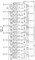
- FIG. 4 illustrates a multiplexor array circuit 400 in accordance with the present invention that utilizes block processing and look-ahead techniques in the selection (multiplexing) stage to produce a delay on the order of logN.
- the multiplexor array circuit 400 of FIG. 4 groups the multiplexors 331-338 of FIG. 3 into groups of two, and provides an array of multiplexors, in a manner described further below, for selecting the appropriate precomputed value for each block pair independently and concurrently.
- the i 0 1 and i 1 1 inputs of block 311 are grouped with the i 0 2 and i 1 2 inputs of block 312, as shown in FIG. 4.
- the i 0 3 and i 1 3 inputs of block 313 are grouped with the i 0 4 and i 1 4 inputs of block 314 (i 0 5 and i 1 5 inputs are grouped with i 0 6 and i 1 6 inputs, and i 0 7 and i 1 7 inputs are grouped with i 0 8 and i 1 8 inputs in a similar manner).
- the transform operation of the present invention is applied to non-overlapping neighboring multiplexor pairs, in parallel.
- a transformed pair is treated as a single multiplexor with multiple outputs and is again grouped into neighboring pairs.
- This transform and group-in-pairs operation can then be repeated, and the select signals closest to the beginning of the dependency chain, such as y 0 in FIG. 4, will double its direct control distance each time.
- the entire dependency chain can be computed in D steps, where D is the tree depth and is equal to logN (because the select signal propagates a distance of 2 logN equal to N).
- the output of block 311 (FIG. 3) is determined by the two possible values i 0 1 and i 1 1 and the select signal, y 0 0 .
- the output of each subsequent block 312-318 (FIG. 3) is determined by the two possible input values i 0 j and i 1 j and the output of the previous block 311-317.
- the present invention utilizes look-ahead techniques in the selection stage to produce a delay on the order of logN.
- the correct value is assumed to be i 1 k (i 1 1 , i 1 3 , i 1 5 , i 1 7 ), and the i 1 k value is applied to the corresponding multiplexors 411, 413, 415, 417 in the first row of each block pair, as shown in FIG. 4.
- the i 1 k value selects i 0 2 or i i 2 for multiplexor 411, i 0 4 or i 1 4 for multiplexor 413, i 0 6 or i 1 6 for multiplexor 415, and i 0 8 or i 1 8 for multiplexor 417.
- the alternate correct value (in the two-level illustration) is also assumed to be i 0 k (i 0 1 , i 0 3 , i 0 5 , i 0 7 ), and the i 0 k value is applied to the corresponding multiplexors 412, 414, 416, 417 in the first row of each block pair, as shown in FIG. 4.
- the i 0 k value selects i 0 2 or i 1 2 for multiplexor 412, i 0 4 or i 1 4 for multiplexor 414, i 0 6 or i 1 6 for multiplexor 416, and i 0 8 or i 1 8 for multiplexor 418.
- the output of the multiplexors 411, 413, 415, 417 contain the correct output value if the corresponding i 1 1 , i 1 3 , i 1 5 , i 1 7 value is the correct value, or (ii) the output of the multiplexors 412, 414, 416, 418 contain the correct output value if the corresponding i 0 1 , i 0 3 , i 0 5 , i 0 7 value is the correct value.
- the outputs of the multiplexors 411, 412 represent the possible values of output y 2 of the block 312 (FIG. 3).
- multiplexors 411 or 412 for the first block pair or multiplexors 415 or 416 for the third block pair contains the final correct value remains unknown.
- multiplexors 411 and 415 contain the correct value and the corresponding value is applied to multiplexors 421 and 423 in the second block pair and multiplexors 425 and 427 in the fourth block pair.
- multiplexors 412 and 416 contain the correct value and the corresponding value is applied to multiplexors 422 and 424 in the second block pair and multiplexors 426 and 428 in the fourth block pair.
- the output of the multiplexor 411 selects the outputs of the multiplexors 421 and 423 as the y 3 and y 4 outputs.
- the output of the multiplexor 412 selects the outputs of the multiplexors 422 and 424 as the y 3 and y 4 outputs.
- the output of multiplexor 421 and 422 represent the possible values of output y 3 of the block 313 (FIG. 3).
- the output of multiplexor 423 and 424 represent the possible values of output y 4 of the block 314 (FIG. 3).
- the choices for y1, y2, y3, y4 at this point are solely determined by y 0 . In other words, the distance under the direct control of y 0 is doubled to 4 blocks.
- y 0 the distance under the direct control of y 0 is doubled to 4 blocks.
- t equal to three multiplexor delay times, all eight output values are directly controlled (selected) by y 0 , with the selection being performed by the last row of multiplexors.
- FIG. 5 illustrates a decision-feedback equalizer (DFE) 500 in accordance with the present invention having a delay on the order of logN.
- the multiplexor array circuit 500 of FIG. 5 is a simplified version of the multiplexor array circuit 400 of FIG. 4.
- the first multiplexor 511 of the multiplexor array circuit 500 selects the correct value for the first stage.
- the simplified architecture is achieved by a utilizing a multiplexor 511 at the first stage, controlled by the select signal y 0 0 .
- the complexity of the multiplexor array circuit 500 is logN*N -N+2 multiplexors, compared with a complexity of N*logN +N for the multiplexor array circuit 400 of FIG. 4. Savings are more significant for small N.
- pipeline latches can be added after any row of multiplexors in the multiplexor array circuit 400 of FIG. 4. Specifically, since there are no dependencies from one row of the multiplexor array 400 to another row, pipeline latches can be added after any row of multiplexors in the multiplexor array circuit 400 of FIG. 4. Thus, each segment of the multiplexor array 400 can be processed simultaneously.
- the number of pipeline segments that can be formed is between 2 and logN.
- the multiplexor array 400 is divided into two segments after the second row of multiplexors, utilizing pipelining techniques.
- the architecture has the most relaxed critical path timing constraint, with just a single multiplexor delay plus one register latch delay. It is noted that while the critical path seems to be equal to that of a traditional look-ahead implementation, such as those described in K. Parhi, "Pipelining in Algorithm with Quantizer Loops". IEEE Transactions on Circuits and Systems, Vol. 38, No. 7, 745-54 (July 1991), incorporated by reference above, the clock is operated at a reduced frequency of f/N.
- the DFE architecture shown in FIGS. 4 and 5 thus allows DFEs to operate at a very high speed. In theory, the architecture of the present invention removes the limit on how fast a DFE can operate.
Landscapes
- Engineering & Computer Science (AREA)
- Power Engineering (AREA)
- Computer Networks & Wireless Communication (AREA)
- Signal Processing (AREA)
- Cable Transmission Systems, Equalization Of Radio And Reduction Of Echo (AREA)
- Advance Control (AREA)
- Feedback Control In General (AREA)
Applications Claiming Priority (2)
| Application Number | Priority Date | Filing Date | Title |
|---|---|---|---|
| US326781 | 1999-06-04 | ||
| US09/326,781 US6192072B1 (en) | 1999-06-04 | 1999-06-04 | Parallel processing decision-feedback equalizer (DFE) with look-ahead processing |
Publications (3)
| Publication Number | Publication Date |
|---|---|
| EP1058431A2 true EP1058431A2 (fr) | 2000-12-06 |
| EP1058431A3 EP1058431A3 (fr) | 2003-12-10 |
| EP1058431B1 EP1058431B1 (fr) | 2007-10-24 |
Family
ID=23273693
Family Applications (1)
| Application Number | Title | Priority Date | Filing Date |
|---|---|---|---|
| EP00304653A Expired - Lifetime EP1058431B1 (fr) | 1999-06-04 | 2000-05-31 | Egaliseur à décision récursive avec traitement à la fois en parallèle et à prévision |
Country Status (4)
| Country | Link |
|---|---|
| US (1) | US6192072B1 (fr) |
| EP (1) | EP1058431B1 (fr) |
| CA (1) | CA2310190C (fr) |
| DE (1) | DE60036834T2 (fr) |
Cited By (6)
| Publication number | Priority date | Publication date | Assignee | Title |
|---|---|---|---|---|
| EP1355462A3 (fr) * | 2002-01-28 | 2006-10-04 | Broadcom Corporation | Traitement pipeline en parallèle de boucles de rétroaction dans un égaliseur à décisions récursives |
| US7239652B2 (en) | 2002-01-28 | 2007-07-03 | Broadcom Corporation | Pipelining of multiplexer loops in a digital circuit |
| DE112004002410B4 (de) * | 2003-12-19 | 2011-06-01 | Intel Corporation, Santa Clara | Feedback-Filter |
| DE102004047702B4 (de) * | 2004-09-30 | 2015-02-05 | Lantiq Deutschland Gmbh | Verfahren und Vorrichtung zur Bestimmung eines Schätzfehlers eines Entscheiders sowie Entzerrer |
| CN108886503A (zh) * | 2016-03-29 | 2018-11-23 | 赛灵思公司 | 判决反馈均衡器 |
| EP4572244A1 (fr) * | 2023-12-15 | 2025-06-18 | INTEL Corporation | Arbre d'égaliseur à rétroaction numérique (dfe) à décision anticipée |
Families Citing this family (27)
| Publication number | Priority date | Publication date | Assignee | Title |
|---|---|---|---|---|
| US6618698B1 (en) * | 1999-08-12 | 2003-09-09 | Quickturn Design Systems, Inc. | Clustered processors in an emulation engine |
| US6940924B1 (en) * | 2000-08-15 | 2005-09-06 | Agere Systems Inc. | Signal detection based on channel estimation |
| US20030174766A1 (en) * | 2001-12-17 | 2003-09-18 | Nahum Don | Signal quality indicator |
| US7245686B2 (en) * | 2001-12-17 | 2007-07-17 | Mysticom Ltd. | Fast skew detector |
| JP4136517B2 (ja) * | 2002-07-31 | 2008-08-20 | 株式会社日立製作所 | 移動端末 |
| US7177352B1 (en) | 2004-05-28 | 2007-02-13 | Pmc-Sierra, Inc. | Pre-cursor inter-symbol interference cancellation |
| US7574146B2 (en) * | 2004-07-09 | 2009-08-11 | Infinera Corporation | Pattern-dependent error counts for use in correcting operational parameters in an optical receiver |
| US20070014345A1 (en) * | 2005-07-13 | 2007-01-18 | Leanics Corporation | Low complexity Tomlinson-Harashima precoders |
| US7669092B2 (en) | 2007-02-26 | 2010-02-23 | Micron Technology, Inc. | Apparatus, method, and system of NAND defect management |
| US20080225950A1 (en) * | 2007-03-13 | 2008-09-18 | Sony Corporation | Scalable architecture for video codecs |
| TWI372517B (en) * | 2008-10-13 | 2012-09-11 | Realtek Semiconductor Corp | Equalizer and method for configuring the equalizer |
| US8428113B1 (en) | 2009-01-23 | 2013-04-23 | Pmc-Sierra, Inc. | Equalizer for heavily clipped or compressed communications signals |
| US9049503B2 (en) * | 2009-03-17 | 2015-06-02 | The Hong Kong Polytechnic University | Method and system for beamforming using a microphone array |
| US8644369B1 (en) | 2009-12-01 | 2014-02-04 | Pmc-Sierra, Inc. | Equalizer adaptation for heavily compressed or clipped communications signals |
| JP5605064B2 (ja) * | 2010-08-04 | 2014-10-15 | 富士通株式会社 | 判定帰還等化回路、受信回路、及び判定帰還等化処理方法 |
| US8611473B1 (en) | 2010-12-15 | 2013-12-17 | Pmc-Sierra, Inc. | Reduction of correlated channel impairments |
| US8699558B1 (en) | 2011-02-25 | 2014-04-15 | Pmc-Sierra Us, Inc. | Decoupling and pipelining of multiplexer loop in parallel processing decision-feedback circuits |
| US9071479B2 (en) * | 2012-08-24 | 2015-06-30 | Credo Semiconductor (Hong Kong) Limited | High-speed parallel decision feedback equalizer |
| US9184948B2 (en) | 2013-05-28 | 2015-11-10 | Globalfoundries U.S. 2 Llc | Decision feedback equalizer (‘DFE’) with a plurality of independently-controlled isolated power domains |
| US9699007B2 (en) * | 2015-08-31 | 2017-07-04 | Huawei Technologies Co., Ltd. | Pipeline multiplexer loop architecture for decision feedback equalizer circuits |
| US9935800B1 (en) | 2016-10-04 | 2018-04-03 | Credo Technology Group Limited | Reduced complexity precomputation for decision feedback equalizer |
| US11398932B2 (en) | 2018-06-27 | 2022-07-26 | Rambus Inc. | Methods and circuits for decision-feedback equalization using compensated decision regions |
| US11405242B2 (en) | 2018-07-02 | 2022-08-02 | Rambus Inc. | Methods and circuits for decision-feedback equalization with early high-order-symbol detection |
| US10728059B1 (en) | 2019-07-01 | 2020-07-28 | Credo Technology Group Limited | Parallel mixed-signal equalization for high-speed serial link |
| US11171816B2 (en) * | 2019-08-07 | 2021-11-09 | Mellanox Technologies, Ltd. | Parallel decision feedback equalizer partitioned for high throughput |
| US11714620B1 (en) | 2022-01-14 | 2023-08-01 | Triad National Security, Llc | Decoupling loop dependencies using buffers to enable pipelining of loops |
| KR20240172878A (ko) | 2023-06-02 | 2024-12-10 | 삼성전자주식회사 | 고속 결정 피드백 등화기를 포함하는 수신기, 통신 시스템 및 그것의 동작 방법 |
Family Cites Families (3)
| Publication number | Priority date | Publication date | Assignee | Title |
|---|---|---|---|---|
| US5027369A (en) * | 1990-03-26 | 1991-06-25 | Motorola, Inc. | Rapid convergence decision feedback equalizer |
| US5642382A (en) * | 1995-03-01 | 1997-06-24 | Hitachi America, Ltd. | Fir filters with multiplexed inputs suitable for use in reconfigurable adaptive equalizers |
| KR0162340B1 (ko) * | 1995-04-28 | 1998-12-01 | 구자홍 | 디지탈 통신 시스템의 고스트 제거 등화기 |
-
1999
- 1999-06-04 US US09/326,781 patent/US6192072B1/en not_active Expired - Lifetime
-
2000
- 2000-05-29 CA CA002310190A patent/CA2310190C/fr not_active Expired - Fee Related
- 2000-05-31 DE DE60036834T patent/DE60036834T2/de not_active Expired - Lifetime
- 2000-05-31 EP EP00304653A patent/EP1058431B1/fr not_active Expired - Lifetime
Cited By (8)
| Publication number | Priority date | Publication date | Assignee | Title |
|---|---|---|---|---|
| EP1355462A3 (fr) * | 2002-01-28 | 2006-10-04 | Broadcom Corporation | Traitement pipeline en parallèle de boucles de rétroaction dans un égaliseur à décisions récursives |
| US7239652B2 (en) | 2002-01-28 | 2007-07-03 | Broadcom Corporation | Pipelining of multiplexer loops in a digital circuit |
| US7333580B2 (en) | 2002-01-28 | 2008-02-19 | Broadcom Corporation | Pipelined parallel processing of feedback loops in a digital circuit |
| DE112004002410B4 (de) * | 2003-12-19 | 2011-06-01 | Intel Corporation, Santa Clara | Feedback-Filter |
| DE102004047702B4 (de) * | 2004-09-30 | 2015-02-05 | Lantiq Deutschland Gmbh | Verfahren und Vorrichtung zur Bestimmung eines Schätzfehlers eines Entscheiders sowie Entzerrer |
| CN108886503A (zh) * | 2016-03-29 | 2018-11-23 | 赛灵思公司 | 判决反馈均衡器 |
| CN108886503B (zh) * | 2016-03-29 | 2021-08-24 | 赛灵思公司 | 判决反馈均衡器 |
| EP4572244A1 (fr) * | 2023-12-15 | 2025-06-18 | INTEL Corporation | Arbre d'égaliseur à rétroaction numérique (dfe) à décision anticipée |
Also Published As
| Publication number | Publication date |
|---|---|
| DE60036834D1 (de) | 2007-12-06 |
| US6192072B1 (en) | 2001-02-20 |
| CA2310190A1 (fr) | 2000-12-04 |
| EP1058431B1 (fr) | 2007-10-24 |
| EP1058431A3 (fr) | 2003-12-10 |
| DE60036834T2 (de) | 2008-08-07 |
| CA2310190C (fr) | 2004-04-06 |
Similar Documents
| Publication | Publication Date | Title |
|---|---|---|
| EP1058431B1 (fr) | Egaliseur à décision récursive avec traitement à la fois en parallèle et à prévision | |
| US7158566B2 (en) | High-speed adaptive interconnect architecture with nonlinear error functions | |
| EP1430672B1 (fr) | Calcul rapide de coefficients d egaliseur a decision retroac tive | |
| US9935800B1 (en) | Reduced complexity precomputation for decision feedback equalizer | |
| US9071479B2 (en) | High-speed parallel decision feedback equalizer | |
| US7616686B2 (en) | Method and apparatus for generating one or more clock signals for a decision-feedback equalizer using DFE detected data | |
| US8379711B2 (en) | Methods and apparatus for decision-feedback equalization with oversampled phase detector | |
| JP3459879B2 (ja) | デジタル通信レシーバー用改良型検知 | |
| EP1365554A1 (fr) | Calcul de coefficients pour un égaliseur à rétroaction de décision et à délai variable | |
| WO2003026237A2 (fr) | Calcul rapide de coefficients d'egaliseur a decision retroactive mimo | |
| EP1264455A2 (fr) | Architecture pour estimation de sequence a decision retroactive a tres grande vitesse | |
| CN101567862B (zh) | 用于通信接收器中的均衡系统与执行均衡的方法 | |
| CN114337602B (zh) | 使用部分乘积的组合近似求和的数字滤波 | |
| Oh et al. | Low complexity design of high speed parallel decision feedback equalizers | |
| US7693233B2 (en) | Parallel Tomlinson-Harashima precoders | |
| US20060056521A1 (en) | High-speed precoders for communication systems | |
| EP0800735B1 (fr) | Egalisation adaptative destinee a des systemes de transmission de classe iv a reponse partielle | |
| US20040120394A1 (en) | Decision-feedback equalizer | |
| US6765958B1 (en) | High-speed adaptive interconnect architecture | |
| US6694280B2 (en) | Method for overflow testing of a blind equalizer | |
| US20070014345A1 (en) | Low complexity Tomlinson-Harashima precoders | |
| Yu et al. | An arbitrarily fast block processing architecture for decision feedback equalizers | |
| Gu et al. | Design of Parallel Tomlinson–Harashima Precoders | |
| Souza et al. | Multi-split equalizers for HDSL channels | |
| EP1145511A2 (fr) | Demodulateur pour un emetteur-recepteur a paires multiplesgigabinaire |
Legal Events
| Date | Code | Title | Description |
|---|---|---|---|
| PUAI | Public reference made under article 153(3) epc to a published international application that has entered the european phase |
Free format text: ORIGINAL CODE: 0009012 |
|
| AK | Designated contracting states |
Kind code of ref document: A2 Designated state(s): AT BE CH CY DE DK ES FI FR GB GR IE IT LI LU MC NL PT SE |
|
| AX | Request for extension of the european patent |
Free format text: AL;LT;LV;MK;RO;SI |
|
| PUAL | Search report despatched |
Free format text: ORIGINAL CODE: 0009013 |
|
| AK | Designated contracting states |
Kind code of ref document: A3 Designated state(s): AT BE CH CY DE DK ES FI FR GB GR IE IT LI LU MC NL PT SE |
|
| AX | Request for extension of the european patent |
Extension state: AL LT LV MK RO SI |
|
| 17P | Request for examination filed |
Effective date: 20040609 |
|
| AKX | Designation fees paid |
Designated state(s): DE FR GB |
|
| GRAP | Despatch of communication of intention to grant a patent |
Free format text: ORIGINAL CODE: EPIDOSNIGR1 |
|
| GRAS | Grant fee paid |
Free format text: ORIGINAL CODE: EPIDOSNIGR3 |
|
| GRAA | (expected) grant |
Free format text: ORIGINAL CODE: 0009210 |
|
| AK | Designated contracting states |
Kind code of ref document: B1 Designated state(s): DE FR GB |
|
| REG | Reference to a national code |
Ref country code: GB Ref legal event code: FG4D |
|
| REF | Corresponds to: |
Ref document number: 60036834 Country of ref document: DE Date of ref document: 20071206 Kind code of ref document: P |
|
| ET | Fr: translation filed | ||
| PLBE | No opposition filed within time limit |
Free format text: ORIGINAL CODE: 0009261 |
|
| STAA | Information on the status of an ep patent application or granted ep patent |
Free format text: STATUS: NO OPPOSITION FILED WITHIN TIME LIMIT |
|
| 26N | No opposition filed |
Effective date: 20080725 |
|
| PGFP | Annual fee paid to national office [announced via postgrant information from national office to epo] |
Ref country code: FR Payment date: 20140509 Year of fee payment: 15 |
|
| REG | Reference to a national code |
Ref country code: DE Ref legal event code: R082 Ref document number: 60036834 Country of ref document: DE Representative=s name: DILG HAEUSLER SCHINDELMANN PATENTANWALTSGESELL, DE |
|
| PGFP | Annual fee paid to national office [announced via postgrant information from national office to epo] |
Ref country code: GB Payment date: 20150424 Year of fee payment: 16 |
|
| REG | Reference to a national code |
Ref country code: FR Ref legal event code: ST Effective date: 20160129 |
|
| PG25 | Lapsed in a contracting state [announced via postgrant information from national office to epo] |
Ref country code: FR Free format text: LAPSE BECAUSE OF NON-PAYMENT OF DUE FEES Effective date: 20150601 |
|
| GBPC | Gb: european patent ceased through non-payment of renewal fee |
Effective date: 20160531 |
|
| PG25 | Lapsed in a contracting state [announced via postgrant information from national office to epo] |
Ref country code: GB Free format text: LAPSE BECAUSE OF NON-PAYMENT OF DUE FEES Effective date: 20160531 |
|
| REG | Reference to a national code |
Ref country code: DE Ref legal event code: R082 Ref document number: 60036834 Country of ref document: DE Representative=s name: DILG HAEUSLER SCHINDELMANN PATENTANWALTSGESELL, DE Ref country code: DE Ref legal event code: R081 Ref document number: 60036834 Country of ref document: DE Owner name: AVAGO TECHNOLOGIES GENERAL IP (SINGAPORE) PTE., SG Free format text: FORMER OWNER: LUCENT TECHNOLOGIES INC., MURRAY HILL, N.J., US Ref country code: DE Ref legal event code: R081 Ref document number: 60036834 Country of ref document: DE Owner name: AVAGO TECHNOLOGIES INTERNATIONAL SALES PTE. LT, SG Free format text: FORMER OWNER: LUCENT TECHNOLOGIES INC., MURRAY HILL, N.J., US |
|
| REG | Reference to a national code |
Ref country code: DE Ref legal event code: R081 Ref document number: 60036834 Country of ref document: DE Owner name: AVAGO TECHNOLOGIES INTERNATIONAL SALES PTE. LT, SG Free format text: FORMER OWNER: AVAGO TECHNOLOGIES GENERAL IP (SINGAPORE) PTE. LTD., SINGAPORE, SG Ref country code: DE Ref legal event code: R082 Ref document number: 60036834 Country of ref document: DE Representative=s name: DILG HAEUSLER SCHINDELMANN PATENTANWALTSGESELL, DE |
|
| PGFP | Annual fee paid to national office [announced via postgrant information from national office to epo] |
Ref country code: DE Payment date: 20190530 Year of fee payment: 20 |
|
| REG | Reference to a national code |
Ref country code: DE Ref legal event code: R071 Ref document number: 60036834 Country of ref document: DE |