EP1058475A2 - Equipment de brassage optique - Google Patents
Equipment de brassage optique Download PDFInfo
- Publication number
- EP1058475A2 EP1058475A2 EP00109176A EP00109176A EP1058475A2 EP 1058475 A2 EP1058475 A2 EP 1058475A2 EP 00109176 A EP00109176 A EP 00109176A EP 00109176 A EP00109176 A EP 00109176A EP 1058475 A2 EP1058475 A2 EP 1058475A2
- Authority
- EP
- European Patent Office
- Prior art keywords
- optical
- wavelength
- control light
- light
- output
- Prior art date
- Legal status (The legal status is an assumption and is not a legal conclusion. Google has not performed a legal analysis and makes no representation as to the accuracy of the status listed.)
- Granted
Links
Images
















Classifications
-
- H—ELECTRICITY
- H04—ELECTRIC COMMUNICATION TECHNIQUE
- H04Q—SELECTING
- H04Q11/00—Selecting arrangements for multiplex systems
- H04Q11/0001—Selecting arrangements for multiplex systems using optical switching
- H04Q11/0005—Switch and router aspects
-
- H—ELECTRICITY
- H04—ELECTRIC COMMUNICATION TECHNIQUE
- H04J—MULTIPLEX COMMUNICATION
- H04J14/00—Optical multiplex systems
- H04J14/02—Wavelength-division multiplex systems
- H04J14/0201—Add-and-drop multiplexing
- H04J14/0202—Arrangements therefor
- H04J14/0204—Broadcast and select arrangements, e.g. with an optical splitter at the input before adding or dropping
-
- H—ELECTRICITY
- H04—ELECTRIC COMMUNICATION TECHNIQUE
- H04J—MULTIPLEX COMMUNICATION
- H04J14/00—Optical multiplex systems
- H04J14/02—Wavelength-division multiplex systems
- H04J14/0201—Add-and-drop multiplexing
- H04J14/0202—Arrangements therefor
- H04J14/0205—Select and combine arrangements, e.g. with an optical combiner at the output after adding or dropping
-
- H—ELECTRICITY
- H04—ELECTRIC COMMUNICATION TECHNIQUE
- H04J—MULTIPLEX COMMUNICATION
- H04J14/00—Optical multiplex systems
- H04J14/02—Wavelength-division multiplex systems
- H04J14/0201—Add-and-drop multiplexing
- H04J14/0202—Arrangements therefor
- H04J14/0213—Groups of channels or wave bands arrangements
-
- H—ELECTRICITY
- H04—ELECTRIC COMMUNICATION TECHNIQUE
- H04Q—SELECTING
- H04Q11/00—Selecting arrangements for multiplex systems
- H04Q11/0001—Selecting arrangements for multiplex systems using optical switching
- H04Q11/0005—Switch and router aspects
- H04Q2011/0007—Construction
- H04Q2011/0009—Construction using wavelength filters
-
- H—ELECTRICITY
- H04—ELECTRIC COMMUNICATION TECHNIQUE
- H04Q—SELECTING
- H04Q11/00—Selecting arrangements for multiplex systems
- H04Q11/0001—Selecting arrangements for multiplex systems using optical switching
- H04Q11/0005—Switch and router aspects
- H04Q2011/0007—Construction
- H04Q2011/0011—Construction using wavelength conversion
-
- H—ELECTRICITY
- H04—ELECTRIC COMMUNICATION TECHNIQUE
- H04Q—SELECTING
- H04Q11/00—Selecting arrangements for multiplex systems
- H04Q11/0001—Selecting arrangements for multiplex systems using optical switching
- H04Q11/0005—Switch and router aspects
- H04Q2011/0007—Construction
- H04Q2011/0015—Construction using splitting combining
-
- H—ELECTRICITY
- H04—ELECTRIC COMMUNICATION TECHNIQUE
- H04Q—SELECTING
- H04Q11/00—Selecting arrangements for multiplex systems
- H04Q11/0001—Selecting arrangements for multiplex systems using optical switching
- H04Q11/0005—Switch and router aspects
- H04Q2011/0007—Construction
- H04Q2011/0016—Construction using wavelength multiplexing or demultiplexing
-
- H—ELECTRICITY
- H04—ELECTRIC COMMUNICATION TECHNIQUE
- H04Q—SELECTING
- H04Q11/00—Selecting arrangements for multiplex systems
- H04Q11/0001—Selecting arrangements for multiplex systems using optical switching
- H04Q11/0005—Switch and router aspects
- H04Q2011/0007—Construction
- H04Q2011/0024—Construction using space switching
-
- H—ELECTRICITY
- H04—ELECTRIC COMMUNICATION TECHNIQUE
- H04Q—SELECTING
- H04Q11/00—Selecting arrangements for multiplex systems
- H04Q11/0001—Selecting arrangements for multiplex systems using optical switching
- H04Q11/0005—Switch and router aspects
- H04Q2011/0037—Operation
- H04Q2011/0049—Crosstalk reduction; Noise; Power budget
Definitions
- OXC optical cross-connect equipment
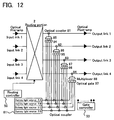
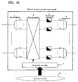
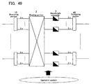
- the routing portion includes; a control light generator for generating control lights each corresponding to the signal light; a route switching means for switching signal lights having a plurality of wavelengths split by the demultiplexer to output; an optical amplification means for amplifying each signal light having each plurality of wavelengths output from the route switching means; a control light insertion portion for inserting the control light generated by the control light generator into an output of the optical amplification means; and a wavelength selection means for selecting an output of the control light insertion portion having a wavelength assigned to the wavelength selection means to output.
- the routing portion includes; a control light generator for generating control lights respectively corresponding to the signal lights; a route switching means for switching a route of the signal light having a plurality of wavelengths each split by the demultiplexer; a control light insertion portion connected at the preceding stage of the route switching means for inserting the control light generated by the control light generator into the signal light having a plurality of wavelengths; an optical amplification means for amplifying an output of the route switching means; a wavelength selection means for selecting an output of the optical amplification means having a wavelength assigned to the wavelength selection means to output.
- FIG. 43 a state of the network system after a switchover is illustrated against a previous state shown in FIG. 42.
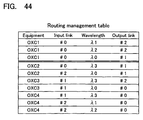
- transmission is carried out using wavelengths ⁇ 1 and ⁇ 2 through a link between optical cross-connect equipment OXC1 and OXC4.
- OXC1 and OXC4 On occurrence of failure (at the point marked X) which causes the link unusable, a transmission link using wavelengths ⁇ 1 and ⁇ 2 is switched to a diversion transmission link from OXC1 through OXC2, OXC3 and OXC4 using standby wavelengths, as shown in FIG. 43.
- communication from OXC1 to OXC2 is carried out using multi-wavelengths ⁇ A, ⁇ B, ⁇ C and ⁇ 4.
- communication from OXC2 to OXC3 is carried out using multi-wavelengths ⁇ A, ⁇ B, ⁇ 3 and ⁇ 4
- communication from OXC3 to OXC4 using multi-wavelengths ⁇ A, ⁇ B, ⁇ 3 and ⁇ D
- communication from OXC1 to OXC4 is carried out using multi-wavelengths ⁇ 1, ⁇ 2, ⁇ C and ⁇ D.
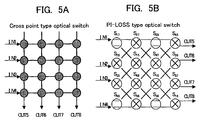
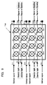
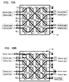
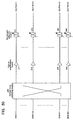
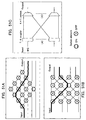
- FIGS. 10A and 10B a concrete operation example when using 4x4 PI-LOSS optical matrix switch 1-a in routing portion 2 is illustrated.
- FIG. 10A there is shown a case that no optical signal is being transmitted on any of the input links. In this case, optical signals from dummy light sources 61 are controlled to route to each output port.
- FIG. 10B another example is shown that an optical signal is input from a link to input port 1-i of PI-LOSS optical matrix switch 1-a, and that no optical signal is input from links to other input ports 2-i to 4-i. In this case, optical signal from the optical link connected to input port 1-i is routed to output port 3-o.
- Optical signal outputs having wavelengths ⁇ 0, ⁇ 1, ⁇ 2 and ⁇ 3 from dummy light sources 61 are multiplexed by multiplexer 8 to be branched by optical coupler 9 to respective wavelength filters 91-94.
- each of wavelength filters 91-94 is a variable wavelength filter to select one or more wavelengths at a time using, for example, an AOTF (acoustic optical tunable filter).
- error rate measuring detectors 121-124 PN pattern signals are received to compare with the received electric signals having been synchronized in PN synchronization detectors 111-114. Then error rate is derived from the rate of mismatched patterns.
- Wavelength selection means 311 in normal cases supervises optical signals branched by optical branching means 316 in controller 317 to perform feedback control (automatic frequency control: hereafter referred to as AFC) of transmitted wavelength in wavelength selector 315 to an optimum wavelength position.
- AFC automatic frequency control
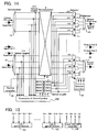
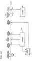
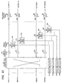
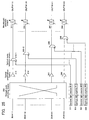
- optical route selection means 219-1, 219-2 and 245-248 in the configuration as shown in FIG. 25, and optical multiplexing means 602 and optical branching means 603 as shown in FIG. 27.
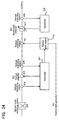
- the embodiment has a configuration in which the features in both the embodiments shown in FIGS. 23 and 27 are introduced. Namely, the configuration of the embodiment comprises optical combining means 711-714 to 741-744 in the embodiment shown in FIG. 23, optical multiplexing means 602 and optical branching means 603. A detailed configuration for a single port is substantially the same as the configuration shown in FIG. 24, and is therefore omitted here.
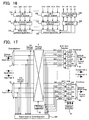
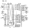
- a switchover from signal light to control light is carried out in optical amplification means 211 without producing a shutdown during a transition state from the time while signal is being input to optical amplification means 211 to the time of the input stoppage.
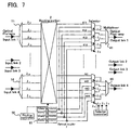
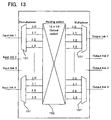
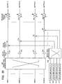
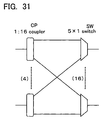
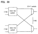
- FIG. 39 a configuration example of optical route switching means 200 is shown, in which a function of control light insertion portion 202 is provided.
- the switch is configured with two (2) sets of 16 x 16 switches and sixteen (16) sets of 2 x 1 switches which are connected as shown in FIG. 39.
- a switch having 32 x 16 components is configured.
Landscapes
- Engineering & Computer Science (AREA)
- Computer Networks & Wireless Communication (AREA)
- Optical Communication System (AREA)
- Use Of Switch Circuits For Exchanges And Methods Of Control Of Multiplex Exchanges (AREA)
Applications Claiming Priority (2)
| Application Number | Priority Date | Filing Date | Title |
|---|---|---|---|
| JP11153065A JP2000341728A (ja) | 1999-05-31 | 1999-05-31 | 光クロスコネクト装置 |
| JP15306599 | 1999-05-31 |
Publications (3)
| Publication Number | Publication Date |
|---|---|
| EP1058475A2 true EP1058475A2 (fr) | 2000-12-06 |
| EP1058475A3 EP1058475A3 (fr) | 2004-01-07 |
| EP1058475B1 EP1058475B1 (fr) | 2008-01-02 |
Family
ID=15554227
Family Applications (1)
| Application Number | Title | Priority Date | Filing Date |
|---|---|---|---|
| EP00109176A Expired - Lifetime EP1058475B1 (fr) | 1999-05-31 | 2000-05-08 | Equipement de brassage optique |
Country Status (4)
| Country | Link |
|---|---|
| US (1) | US6522803B1 (fr) |
| EP (1) | EP1058475B1 (fr) |
| JP (1) | JP2000341728A (fr) |
| DE (1) | DE60037616D1 (fr) |
Cited By (4)
| Publication number | Priority date | Publication date | Assignee | Title |
|---|---|---|---|---|
| FR2834402A1 (fr) * | 2002-01-03 | 2003-07-04 | Cit Alcatel | Dispositif de commutation optique et procede de commande de ce dispositif |
| EP1981184A3 (fr) * | 2007-04-10 | 2008-12-10 | Huawei Technologies Co., Ltd. | Appareil et procédé de compensation de gain optique d'un câble optique sous-marin |
| WO2013170909A1 (fr) * | 2012-05-15 | 2013-11-21 | Telefonaktiebolaget L M Ericsson (Publ) | Signaux optiques fictifs pour réseau optique |
| CN103493413A (zh) * | 2011-04-20 | 2014-01-01 | 日本电气株式会社 | 具有oadm功能的分歧设备和波分复用光网络系统及其方法 |
Families Citing this family (37)
| Publication number | Priority date | Publication date | Assignee | Title |
|---|---|---|---|---|
| JP2001217778A (ja) * | 2000-02-03 | 2001-08-10 | Kanagawa Acad Of Sci & Technol | 光送受信機 |
| US6907201B1 (en) * | 2000-07-28 | 2005-06-14 | Ciena Corporation | Optical power transient control system and method |
| JP3514220B2 (ja) * | 2000-08-02 | 2004-03-31 | 日本電気株式会社 | 波長分割多重伝送システム、及びこの波長分割多重伝送システムにおけるチャネルの増設方法 |
| US6915078B1 (en) * | 2000-08-15 | 2005-07-05 | Alcatel | Optical frame format |
| FR2816778B1 (fr) * | 2000-11-13 | 2003-02-07 | Cit Alcatel | Dispositif de selection et de conversion longueur d'onde, et matrice de commutation photonique l'incorporant |
| JP4209080B2 (ja) * | 2000-11-29 | 2009-01-14 | 富士通株式会社 | 光クロスコネクト装置及び該装置を有するシステム |
| JP2002315027A (ja) * | 2001-04-18 | 2002-10-25 | Nec Corp | 波長群波長変換器及びそれを用いた波長群交換機 |
| FR2832884B1 (fr) * | 2001-11-27 | 2012-07-27 | Cit Alcatel | Interface dorsale, interface terminale de communication pour vehicule spatial et reseau de communication comprenant de telles interfaces |
| US7146098B1 (en) * | 2001-12-20 | 2006-12-05 | Nortel Networks Limited | Optical protection scheme |
| JP2003199130A (ja) * | 2001-12-27 | 2003-07-11 | Fujitsu Ltd | 光パスクロスコネクト装置及びその切替方法 |
| US6768827B2 (en) * | 2002-01-16 | 2004-07-27 | The Regents Of The University Of California | Integrated optical router |
| US6842554B2 (en) * | 2002-03-29 | 2005-01-11 | Fujitsu Limited | Optical cross-connect device and optical network |
| WO2003105496A1 (fr) | 2002-06-06 | 2003-12-18 | 富士通株式会社 | Controleur permettant de commuter un signal optique multiplexe en longueur d'onde |
| FR2849305B1 (fr) * | 2002-12-24 | 2005-04-29 | Cit Alcatel | Procede et dispositif perfectionnes de controle de la puissance delivree en sortie d'un noeud d'un reseau optique a commutation de bandes de longueurs d'onde |
| US7054519B1 (en) | 2003-03-10 | 2006-05-30 | Active Optical Networks, Inc. | Reconfigurable optical add drop multiplexers with integrated power equalization |
| DE10343615A1 (de) * | 2003-09-20 | 2005-04-14 | Marconi Communications Gmbh | Netzknoten für ein optisches Nachrichtenübertragungsnetz |
| US20060088242A1 (en) * | 2003-12-31 | 2006-04-27 | Vlad Novotny | Optical switches with uniaxial mirrors |
| JP4643645B2 (ja) * | 2004-08-11 | 2011-03-02 | タイコ エレクトロニクス サブシー コミュニケーションズ エルエルシー | 光伝送システムにスペクトル負荷を与えるシステム及び方法 |
| JP2006196938A (ja) * | 2005-01-11 | 2006-07-27 | Kddi Corp | 光ネットワークシステム |
| JP2007274482A (ja) * | 2006-03-31 | 2007-10-18 | Fujitsu Ltd | 光伝送装置 |
| JP5386943B2 (ja) | 2008-11-20 | 2014-01-15 | 富士通株式会社 | 波形制御装置,応答素子モジュール,光スイッチ装置および光スイッチ装置の制御方法 |
| JP5473529B2 (ja) * | 2009-10-21 | 2014-04-16 | 三菱電機株式会社 | ノード装置および光伝送システム |
| JP5648429B2 (ja) * | 2010-11-02 | 2015-01-07 | 富士通株式会社 | 光伝送システム及び光伝送装置 |
| JP5939811B2 (ja) * | 2012-01-26 | 2016-06-22 | 三菱電機株式会社 | 波長多重伝送装置 |
| JP6291799B2 (ja) | 2013-11-13 | 2018-03-14 | 富士通株式会社 | 光伝送装置及び光伝送方法 |
| JP2017168916A (ja) * | 2016-03-14 | 2017-09-21 | 日本電気株式会社 | 光スイッチ、光経路切り替えシステム、及び光経路切り替え方法 |
| US9941991B2 (en) * | 2016-08-29 | 2018-04-10 | Huawei Technologies Co., Ltd. | Method and system for controlling spectral occupancy |
| US10536235B2 (en) * | 2017-05-04 | 2020-01-14 | Ciena Corporation | Logical control seams in optical networks to improve restoration speed or timing for capacity adds |
| US11038615B2 (en) * | 2018-04-16 | 2021-06-15 | Huawei Technologies Co., Ltd. | Fast connection turn-up with path-based dummy lights |
| US10868614B2 (en) * | 2018-09-04 | 2020-12-15 | Ciena Corporation | Optical power replacement for faulted spectrum in channel holder based optical links |
| US10833791B1 (en) | 2019-06-17 | 2020-11-10 | Ciena Corporation | Reducing interference from channel holders in an optical link |
| US11095509B2 (en) * | 2019-09-11 | 2021-08-17 | Huawei Technologies Co., Ltd. | Method and apparatus for interdependent control of amplification and switching state in a photonic switch |
| CN113395128B (zh) * | 2020-03-12 | 2023-12-15 | 华为技术有限公司 | 一种产生假光信号的装置以及级联系统 |
| JP7609272B2 (ja) * | 2021-06-07 | 2025-01-07 | 日本電信電話株式会社 | 波長クロスコネクト装置及び波長クロスコネクト方法 |
| US20240283557A1 (en) * | 2021-06-07 | 2024-08-22 | Nippon Telegraph And Telephone Corporation | Wavelength cross connect device, and wavelength cross connect method |
| JP2023170431A (ja) * | 2022-05-19 | 2023-12-01 | 日本電気株式会社 | スイッチ装置、及びスイッチ方法 |
| CN120825648A (zh) * | 2024-04-12 | 2025-10-21 | 华为技术有限公司 | 一种光通信网络 |
Family Cites Families (11)
| Publication number | Priority date | Publication date | Assignee | Title |
|---|---|---|---|---|
| DE3689583T2 (de) * | 1985-11-22 | 1994-08-25 | Nippon Electric Co | Optisches Wellenlängenmultiplexvermittlungssystem mit Wellenlängenschaltlichtmodulatoren. |
| JP2692316B2 (ja) * | 1989-11-20 | 1997-12-17 | 日本電気株式会社 | 波長分割光交換機 |
| JP3308525B2 (ja) * | 1990-11-30 | 2002-07-29 | 株式会社日立製作所 | ネットワーク |
| US5754320A (en) * | 1995-08-18 | 1998-05-19 | Nippon Telegraph And Telephone Corporation | Optical cross-connect system |
| US5739935A (en) * | 1995-11-14 | 1998-04-14 | Telefonaktiebolaget Lm Ericsson | Modular optical cross-connect architecture with optical wavelength switching |
| US5959767A (en) * | 1996-12-31 | 1999-09-28 | Lucent Technologies | Loss-less optical cross-connect |
| JP3102379B2 (ja) * | 1997-04-30 | 2000-10-23 | 日本電気株式会社 | 波長多重光伝送システム用監視制御方式 |
| JP3060994B2 (ja) * | 1997-05-15 | 2000-07-10 | 日本電気株式会社 | N−wdmシステムにおける出力ポート切替装置 |
| FR2764141B1 (fr) * | 1997-05-29 | 1999-07-23 | Alsthom Cge Alcatel | Systeme de transmission optique a compensation dynamique de la puissance transmise |
| JPH11136214A (ja) * | 1997-10-28 | 1999-05-21 | Matsushita Electric Ind Co Ltd | 波長多重光伝送システム |
| JP4015750B2 (ja) * | 1998-05-14 | 2007-11-28 | 株式会社東芝 | アクティブアレイアンテナシステム |
-
1999
- 1999-05-31 JP JP11153065A patent/JP2000341728A/ja active Pending
-
2000
- 2000-04-26 US US09/558,072 patent/US6522803B1/en not_active Expired - Fee Related
- 2000-05-08 EP EP00109176A patent/EP1058475B1/fr not_active Expired - Lifetime
- 2000-05-08 DE DE60037616T patent/DE60037616D1/de not_active Expired - Lifetime
Cited By (9)
| Publication number | Priority date | Publication date | Assignee | Title |
|---|---|---|---|---|
| FR2834402A1 (fr) * | 2002-01-03 | 2003-07-04 | Cit Alcatel | Dispositif de commutation optique et procede de commande de ce dispositif |
| EP1326473A1 (fr) * | 2002-01-03 | 2003-07-09 | Alcatel | Dispositif de communication optique et procédé de commande de ce dispositif |
| US6836582B2 (en) | 2002-01-03 | 2004-12-28 | Alcatel | Optical switching device and a method of controlling the device |
| EP1981184A3 (fr) * | 2007-04-10 | 2008-12-10 | Huawei Technologies Co., Ltd. | Appareil et procédé de compensation de gain optique d'un câble optique sous-marin |
| CN103493413A (zh) * | 2011-04-20 | 2014-01-01 | 日本电气株式会社 | 具有oadm功能的分歧设备和波分复用光网络系统及其方法 |
| EP2701316A4 (fr) * | 2011-04-20 | 2014-11-19 | Nec Corp | Dispositif de divergence avec fonction oadm et système de réseau optique à multiplexage par répartition en longueurs d'onde et procédé associé |
| US9166726B2 (en) | 2011-04-20 | 2015-10-20 | Nec Corporation | Diverging device with OADM function and wavelength division multiplexing optical network system and method therefor |
| CN103493413B (zh) * | 2011-04-20 | 2017-03-22 | 日本电气株式会社 | 具有oadm功能的分歧设备和波分复用光网络系统及其方法 |
| WO2013170909A1 (fr) * | 2012-05-15 | 2013-11-21 | Telefonaktiebolaget L M Ericsson (Publ) | Signaux optiques fictifs pour réseau optique |
Also Published As
| Publication number | Publication date |
|---|---|
| EP1058475A3 (fr) | 2004-01-07 |
| EP1058475B1 (fr) | 2008-01-02 |
| DE60037616D1 (de) | 2008-02-14 |
| US6522803B1 (en) | 2003-02-18 |
| JP2000341728A (ja) | 2000-12-08 |
Similar Documents
| Publication | Publication Date | Title |
|---|---|---|
| EP1058475B1 (fr) | Equipement de brassage optique | |
| KR100301950B1 (ko) | 광 회선분배 시스템의 입력단자 판별에 의한 광 경로 감시 장치 | |
| US8121477B2 (en) | Optical node apparatus | |
| JP3930952B2 (ja) | 光クロスコネクト装置,光挿入分岐装置および光源装置 | |
| US8457497B2 (en) | Optimized directionless optical add/drop module systems and methods | |
| EP1467591B1 (fr) | Commutateur optique | |
| US12308599B2 (en) | Optical amplifier, optical amplifier equalizing method, and transmission system | |
| US7155124B2 (en) | Loss-less architecture and method for wavelength division multiplexing (WDM) optical networks | |
| JP2001203644A (ja) | 光増幅器および光増幅方法 | |
| US7072585B2 (en) | Per-channel optical amplification using saturation mode | |
| US8189258B2 (en) | Optical amplifier configuration | |
| US11870208B2 (en) | Optical fiber amplifier, optical fiber amplifier control method, and transmission system | |
| GB2324667A (en) | Wavelength multiplexed optical signal amplification control system | |
| JP2003199130A (ja) | 光パスクロスコネクト装置及びその切替方法 | |
| JP7589640B2 (ja) | 光増幅装置、光伝送システム、および光増幅方法 | |
| US6809846B2 (en) | Optical switch and optical network | |
| KR20030014020A (ko) | 고정파장 광원을 이용한 파장변환장치 및 이를 적용한광회선분배시스템 | |
| JPWO2018190240A1 (ja) | 中継器及び中継方法 | |
| JPH11313349A (ja) | 光クロスコネクト制御方式 | |
| EP1033835A2 (fr) | Bureau central optique | |
| JP2002368315A (ja) | 光増幅装置及びそれを用いた光伝送システム | |
| US20050213967A1 (en) | Optical wavelength division multiplexing transmission system | |
| JP7670069B2 (ja) | 光源装置、光装置および制御光生成方法 | |
| WO2022153350A1 (fr) | Dispositif de source de lumière, dispositif optique, procédé de génération de lumière de commande et procédé de génération de lumière de transmission | |
| KR100223053B1 (ko) | 광가입자 전송장치의 다파장 공유 광원발생장치 |
Legal Events
| Date | Code | Title | Description |
|---|---|---|---|
| PUAI | Public reference made under article 153(3) epc to a published international application that has entered the european phase |
Free format text: ORIGINAL CODE: 0009012 |
|
| 17P | Request for examination filed |
Effective date: 20000508 |
|
| AK | Designated contracting states |
Kind code of ref document: A2 Designated state(s): AT BE CH CY DE DK ES FI FR GB GR IE IT LI LU MC NL PT SE |
|
| AX | Request for extension of the european patent |
Free format text: AL;LT;LV;MK;RO;SI |
|
| PUAL | Search report despatched |
Free format text: ORIGINAL CODE: 0009013 |
|
| RIC1 | Information provided on ipc code assigned before grant |
Ipc: 7H 04Q 11/00 A Ipc: 7H 04B 10/17 B |
|
| AK | Designated contracting states |
Kind code of ref document: A3 Designated state(s): AT BE CH CY DE DK ES FI FR GB GR IE IT LI LU MC NL PT SE |
|
| AX | Request for extension of the european patent |
Extension state: AL LT LV MK RO SI |
|
| AKX | Designation fees paid |
Designated state(s): DE FR GB SE |
|
| GRAP | Despatch of communication of intention to grant a patent |
Free format text: ORIGINAL CODE: EPIDOSNIGR1 |
|
| GRAS | Grant fee paid |
Free format text: ORIGINAL CODE: EPIDOSNIGR3 |
|
| GRAA | (expected) grant |
Free format text: ORIGINAL CODE: 0009210 |
|
| AK | Designated contracting states |
Kind code of ref document: B1 Designated state(s): DE FR GB SE |
|
| REG | Reference to a national code |
Ref country code: GB Ref legal event code: FG4D |
|
| REF | Corresponds to: |
Ref document number: 60037616 Country of ref document: DE Date of ref document: 20080214 Kind code of ref document: P |
|
| ET | Fr: translation filed | ||
| PG25 | Lapsed in a contracting state [announced via postgrant information from national office to epo] |
Ref country code: SE Free format text: LAPSE BECAUSE OF FAILURE TO SUBMIT A TRANSLATION OF THE DESCRIPTION OR TO PAY THE FEE WITHIN THE PRESCRIBED TIME-LIMIT Effective date: 20080402 |
|
| PLBE | No opposition filed within time limit |
Free format text: ORIGINAL CODE: 0009261 |
|
| STAA | Information on the status of an ep patent application or granted ep patent |
Free format text: STATUS: NO OPPOSITION FILED WITHIN TIME LIMIT |
|
| 26N | No opposition filed |
Effective date: 20081003 |
|
| PG25 | Lapsed in a contracting state [announced via postgrant information from national office to epo] |
Ref country code: DE Free format text: LAPSE BECAUSE OF FAILURE TO SUBMIT A TRANSLATION OF THE DESCRIPTION OR TO PAY THE FEE WITHIN THE PRESCRIBED TIME-LIMIT Effective date: 20080403 |
|
| PGFP | Annual fee paid to national office [announced via postgrant information from national office to epo] |
Ref country code: FR Payment date: 20090515 Year of fee payment: 10 |
|
| PGFP | Annual fee paid to national office [announced via postgrant information from national office to epo] |
Ref country code: GB Payment date: 20090506 Year of fee payment: 10 |
|
| GBPC | Gb: european patent ceased through non-payment of renewal fee |
Effective date: 20100508 |
|
| REG | Reference to a national code |
Ref country code: FR Ref legal event code: ST Effective date: 20110131 |
|
| PG25 | Lapsed in a contracting state [announced via postgrant information from national office to epo] |
Ref country code: FR Free format text: LAPSE BECAUSE OF NON-PAYMENT OF DUE FEES Effective date: 20100531 |
|
| PG25 | Lapsed in a contracting state [announced via postgrant information from national office to epo] |
Ref country code: GB Free format text: LAPSE BECAUSE OF NON-PAYMENT OF DUE FEES Effective date: 20100508 |