EP1059545A1 - Gruppen-wellenleiter gitter Multiplexer und Demultiplexer - Google Patents
Gruppen-wellenleiter gitter Multiplexer und Demultiplexer Download PDFInfo
- Publication number
- EP1059545A1 EP1059545A1 EP99973331A EP99973331A EP1059545A1 EP 1059545 A1 EP1059545 A1 EP 1059545A1 EP 99973331 A EP99973331 A EP 99973331A EP 99973331 A EP99973331 A EP 99973331A EP 1059545 A1 EP1059545 A1 EP 1059545A1
- Authority
- EP
- European Patent Office
- Prior art keywords
- waveguide
- input
- face
- output
- slab waveguide
- Prior art date
- Legal status (The legal status is an assumption and is not a legal conclusion. Google has not performed a legal analysis and makes no representation as to the accuracy of the status listed.)
- Granted
Links
- 230000003287 optical effect Effects 0.000 claims abstract description 125
- 230000003247 decreasing effect Effects 0.000 claims 1
- 238000001228 spectrum Methods 0.000 abstract description 26
- 230000001419 dependent effect Effects 0.000 abstract description 19
- 230000005684 electric field Effects 0.000 description 27
- 239000006185 dispersion Substances 0.000 description 11
- VYPSYNLAJGMNEJ-UHFFFAOYSA-N Silicium dioxide Chemical compound O=[Si]=O VYPSYNLAJGMNEJ-UHFFFAOYSA-N 0.000 description 8
- 230000005540 biological transmission Effects 0.000 description 6
- 239000000758 substrate Substances 0.000 description 6
- 230000002902 bimodal effect Effects 0.000 description 4
- 238000005253 cladding Methods 0.000 description 4
- 230000006866 deterioration Effects 0.000 description 4
- 239000010410 layer Substances 0.000 description 4
- 238000004088 simulation Methods 0.000 description 4
- 229910052681 coesite Inorganic materials 0.000 description 3
- 239000012792 core layer Substances 0.000 description 3
- 229910052906 cristobalite Inorganic materials 0.000 description 3
- 238000000151 deposition Methods 0.000 description 3
- 230000008021 deposition Effects 0.000 description 3
- 239000011521 glass Substances 0.000 description 3
- 239000002075 main ingredient Substances 0.000 description 3
- 239000000377 silicon dioxide Substances 0.000 description 3
- 229910052682 stishovite Inorganic materials 0.000 description 3
- 229910052905 tridymite Inorganic materials 0.000 description 3
- 230000007423 decrease Effects 0.000 description 2
- 238000010438 heat treatment Methods 0.000 description 2
- 238000000034 method Methods 0.000 description 2
- 239000002019 doping agent Substances 0.000 description 1
- 238000005530 etching Methods 0.000 description 1
- 239000000463 material Substances 0.000 description 1
- 239000013307 optical fiber Substances 0.000 description 1
- 238000000206 photolithography Methods 0.000 description 1
- 238000011160 research Methods 0.000 description 1
- 230000008054 signal transmission Effects 0.000 description 1
- 230000003595 spectral effect Effects 0.000 description 1
Images


Classifications
-
- G—PHYSICS
- G02—OPTICS
- G02B—OPTICAL ELEMENTS, SYSTEMS OR APPARATUS
- G02B6/00—Light guides; Structural details of arrangements comprising light guides and other optical elements, e.g. couplings
- G02B6/10—Light guides; Structural details of arrangements comprising light guides and other optical elements, e.g. couplings of the optical waveguide type
- G02B6/12—Light guides; Structural details of arrangements comprising light guides and other optical elements, e.g. couplings of the optical waveguide type of the integrated circuit kind
- G02B6/12007—Light guides; Structural details of arrangements comprising light guides and other optical elements, e.g. couplings of the optical waveguide type of the integrated circuit kind forming wavelength selective elements, e.g. multiplexer, demultiplexer
- G02B6/12009—Light guides; Structural details of arrangements comprising light guides and other optical elements, e.g. couplings of the optical waveguide type of the integrated circuit kind forming wavelength selective elements, e.g. multiplexer, demultiplexer comprising arrayed waveguide grating [AWG] devices, i.e. with a phased array of waveguides
- G02B6/12016—Light guides; Structural details of arrangements comprising light guides and other optical elements, e.g. couplings of the optical waveguide type of the integrated circuit kind forming wavelength selective elements, e.g. multiplexer, demultiplexer comprising arrayed waveguide grating [AWG] devices, i.e. with a phased array of waveguides characterised by the input or output waveguides, e.g. tapered waveguide ends, coupled together pairs of output waveguides
Definitions
- the present invention relates to an optical multiplexer/demultiplexer for use in optical wavelength (optical frequency) multiplex communication, and more specifically, to an arrayed waveguide grating type optical multiplexer/demultiplexer having a sufficiently flat wavelength-dependent spectrum response in passing channel spacings or wavelength bands.
- optical wavelength multiplex communication system In recent years, in the field of optical communication, researches are eagerly being pursued on optical wavelength multiplex communication system that brings a large increase in transmission capacity.
- the available transmission wavelength range is divided into a plurality of passing channel spacings, and pieces of information, carried by a plurality of lightwave signals of different wavelengths, are transmitted through a single optical fiber.
- an optical multiplexer/demultiplexer for multiplexing lightwaves of different wavelengths (frequencies) and for demultiplexing the wavelength-multiplexed lightwave into the lightwaves of the original wavelengths is used in the optical wavelength multiplex communication.
- the optical multiplexer/demultiplexer is required to be capable of multiplexing and demultiplexing lightwaves having a frequency interval of 100GHz, for instance, which corresponds to a wavelength interval of about 0.8nm in the 1.55 ⁇ m region.
- the oscillating wavelength in the LD light source can deviate from the designed wavelength due to variations in ambient conditions such as temperature and humidity, and can vary with time. Therefore, when the LD light source is used, the wavelength of lightwave to be multiplexed or demultiplexed can vary.
- the spectrum response of the optical multiplexer/demultiplexer in a passing wavelength band (channel spacing) is wavelength-dependent. (Spectrum response will be hereinafter referred to also as wavelength-dependent spectrum response.)
- the loss of the light passing through the optical multiplexer/demultiplexer varies depending on the spectrum response of the optical multiplexer/demultiplexer by the amount corresponding to the variation of the oscillating wavelength of the light source.
- Such variation of loss makes the loss of multiplexed/demultiplexed light ununiform between lightwaves having different wavelengths. This ununiformity causes deterioration in signal-to-noise ratio in the transmission of pieces of information carried by lightwave signals.
- the optical multiplexer/demultiplexer for use in the optical wavelength multiplex communication system is not only required to be able to multiplex and demultiplex many lightwaves of narrow channel spacings, but also required to have a sufficiently flat wavelength-dependent spectrum response in passing channel spacings in the wavelength range used for the multiplex communication.
- An arrayed wavelength grating type optical multiplexer/demultiplexer shown by way of example in FIG. 8 has a plurality of input waveguides 2 formed on a substrate 1.
- the input waveguides 2 are connected to an end face 3a of an input-side slab waveguide 3 having the other end face 3b thereof connected to one-side ends of a plurality of channel waveguides 4a that constitute an arrayed waveguide grating 4.
- the other ends of the channel waveguides 4a are connected to an end face 5a of an output-side slab waveguide 5 having the other end face 5b thereof connected to a plurality of output waveguides 6.
- the input-side slab waveguide 3 has opposite end faces 3a, 3b.
- the end face 3b is formed to be a concave face that has a center of curvature positioned at the center of the other end face 3a.
- the end face 3a is formed to be a concave face having a center of curvature thereof positioned at the middle point of a line connecting the centers of the end faces 3a, 3b.
- the end face 5a of the output-side slab waveguide 5 is formed to be a concave face whose center of curvature is positioned at the center of the other end face 5b
- the end face 5b is formed to be a concave face having a center of curvature thereof positioned at the middle point of a line connecting the centers of the end faces 5a, 5b.
- wavelength-multiplexed light is introduced through an input waveguide 2 connected to a central portion of, preferably, the center of the end face 3a of the input side-slab waveguide 3.
- the wavelength-multiplexed light is incident on the end face 3a of the input-side slab waveguide 3, and diffracted in the slab waveguide 3.
- the channel waveguides 4a that are connected to the other end face 3b of the input-side slab waveguide 3 and that have different waveguide lengths, the light is incident on the end face 5a of the output-side slab waveguide 5, undergoes interference in the slab waveguide 5, and focuses on the other end face 5b of the slab waveguide 5.
- Focusing positions are different according to wavelengths. For example, lightwaves, each having a central wavelength in a corresponding one of the passing channel spacings for the optical multiplexer/demultiplexer, focus on their respective focusing positions on the slab waveguide end face 5b and are taken out through the output waveguides 6 connected to those focusing positions, respectively.
- the multiplexer function signal light beams entering the input waveguides 2 or the output waveguides 6 and having different wavelengths are multiplexed, and the multiplexed signal light is taken out from the input waveguide 2 or the output waveguide 6 that is connected to the center of the input or output side slab waveguide end face 3a or 5b.
- ⁇ denotes the angle of diffraction
- m the order of diffraction
- ⁇ the wavelength of an input lightwave
- n the refractive index of the slab waveguides 3 and 5
- d the pitch between the channel waveguides 4a.
- the focal length of the output-side slab waveguide 5 is denoted by F1
- the position on the slab waveguide end face 5b as viewed in the direction of the width of the slab waveguide 5 is denoted by x1
- the linear dispersion on the end face 3a of the input-side slab waveguide 3 is the same as the linear dispersion on the end face 5b of the output-side slab waveguide 5 expressed by equation (2).
- the electric field distribution of the light that focuses on the focusing position on the end face 5b of the output-side slab waveguide 5 corresponds to the electric field distribution of the input light that is incident on the input-side slab waveguide 3 from the input waveguide 2.
- the broadening of the electric field distribution of the input light is relatively narrow. Therefore, in the conventional arrayed waveguide grating type optical multiplexer/demultiplexer, the broadening of the electric field distribution of the light, which focuses on the focusing position on the end face 5b of the output-side slab waveguide 5 and is taken out through the output waveguides 6 corresponding to those focusing positions, is relatively narrow.
- the broadening of the electric field distribution of the light observed at the focusing position closely relates to the flatness of the wavelength-dependent spectrum response in the passing wavelength band or channel spacing.
- the object of the present invention is to provide an arrayed waveguide grating type optical multiplexer/demultiplexer having a desirable wavelength-dependent spectrum response in passing channel spacings.
- the present invention provides an arrayed waveguide grating type optical multiplexer/demultiplexer in which a diffraction grating side end face of an input-side slab waveguide and a diffraction grating side end face of an output-side slab waveguide are connected by an arrayed waveguide grating comprised of a plurality of channel waveguides, a single or a plurality of input waveguides are connected to a waveguide side end face of the input-side slab waveguide, and a single or a plurality of output waveguides are connected to a waveguide side end face of the output-side slab waveguide.
- the optical multiplexer/demultiplexer is characterized in that a focal length of the diffraction grating side end face of the output-side slab waveguide is longer than a focal length of the waveguide side end face of the input-side slab waveguide.
- the optical multiplexer/demultiplexer of the present invention which includes an arrayed waveguide grating capable of multiplexing lightwaves of narrow channel spacings and demultiplexing a wavelength-multiplexed lightwave made of such lightwaves, is suited to multiplex and demultiplex lightwave signals in an optical wavelength (optical frequency) multiplex communication system using, for signal transmission, the transmission wavelength region divided into a plurality of passing channel spacings.
- the focal length of the output-side slab waveguide end face is longer than the focal length of the input-side slab waveguide end face, the broadening of the electric field distribution of the light observed on the output-side slab waveguide end face is broader than the broadening of the electric field distribution of the light on the input-side slab waveguide end face.
- This improves the flatness of the wavelength-dependent spectrum response in each passing channel spacing for the optical multiplex communication.
- the loss of light can be varied by the deviation of wavelength.
- the variation of the loss of light can cause deterioration in signal-to-noise ratio in the communication system.
- the optical multiplexer/demultiplexer of the present invention having a sufficiently flat wavelength-dependent spectrum response, the wavelength-dependency of the loss of the light passing through the multiplexer/demultiplexer is reduced as long as the deviated central wavelength falls within a region where the wavelength-dependent spectrum response is flat.
- the variation of the loss of light is reduced, and the deterioration in signal-to-noise ratio is reduced.
- the loss of the light, passing through an optical multiplexer/demultiplexer, observed at a wavelength falling within a channel spacing is not larger than that observed at the central wavelength of the channel spacing, for example, by 1dB or more.
- the optical multiplexer/demultiplexer it is desirable for the optical multiplexer/demultiplexer to have a broad 1dB passing band width (1dB channel spacing width).
- the present invention can provide an optical multiplexer/demultiplexer that meets such a requirement, therefore, it can be of great help in constructing an optical wavelength multiplex communication system.
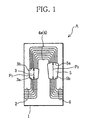
- the optical multiplexer/demultiplexer A has basically the same structure as that of the conventional optical multiplexer/demultiplexer shown in FIG. 8. It comprises input waveguides 2, an input-side slab waveguide 3, an arrayed waveguide grating 4, an output-side slab waveguide 5 and output waveguides 6 that are formed on a substrate 1.
- the diffraction grating 4 is composed of a plurality of channel waveguides 4 of different waveguide lengths.
- the components 2 to 6 of the optical multiplexer/demultiplexer A are connected in the same manner as in the optical multiplexer/demultiplexer of FIG. 8.
- the substrate 1 is, for example, an Si substrate or a glass substrate.
- the input waveguides 2, output waveguides 6, input-side slab waveguide 3, output-side slab waveguide 5 and arrayed waveguide grating 4 are formed, for example, of silica glass into their predetermined shapes, and embedded in a cladding material having a refractive index lower than that of silica glass.
- an end face 3b of the input-side slab waveguide 3 is formed to be a concave face whose center of curvature is positioned at the center of the other end face 3a.
- the end face 3a is formed to be a concave face having a center of curvature thereof positioned at the middle point of a line connecting the centers of the end faces 3a, 3b.
- the focal length of the input-side slab waveguide end face 3b is determined to be, for example, a value F1 that is equal to the focal length of the end faces of the input-side and output-side slab waveguides of the conventional optical multiplexer/demultiplexer shown in FIG. 8.
- An end face 5a of the output-side slab waveguide 5 is formed to be a concave face having a center of curvature thereof positioned at the center of the other end face 5b, and the end face 5b is formed to be a concave face that has a center of curvature at the middle point of a line connecting the centers of the end faces 5a, 5b.
- the focal length of the end face 5a of the output-side slab waveguide 5 is determined to be a value F2 that is larger than the value F1, the focal length of the end face 3b of the input-side slab waveguide 3.
- the optical multiplexer/demultiplexer A has a multiplexer function of multiplexing a plurality of signal lightwaves of different wavelengths introduced through a plurality of input waveguides 2 and taking out a wavelength-multiplexed lightwave through a single output waveguide 6 connected to a central portion, desirably the center of the end face 5b of the output-side slab waveguide 5, and also has a demultiplexer function of demultiplexing a wavelength-multiplexed lightwave introduced through a single output waveguide 6 and taking out a plurality of signal lightwaves through a plurality of input waveguides 2.
- the multiplexer function of the optical multiplexer/demultiplexer A will be mainly explained.
- m denotes the order of diffraction
- ⁇ the wavelength of an input lightwave
- n the refractive index of the slab waveguides 3 and 5
- d the pitch between the channel waveguides 4a.
- the focal lengths of the end faces of the input-side and output-side slab waveguides are determined to be a value F1.
- the position on the slab waveguide end face 5b in the direction of the width of the output-side slab waveguide 5 is denoted by x1
- the linear dispersion on the slab waveguide end face 5b is expressed by equation (2) below, as already mentioned.
- the linear dispersion dx2/d ⁇ in the optical multiplexer/demultiplexer A of the present invention is larger than the linear dispersion dx1/d ⁇ in the conventional optical multiplexer/demultiplexer of FIG. 8.
- the linear dispersion dx1/d ⁇ , dx2/d ⁇ given by equation (2), (3) represents focusing wavelength density on the end face (focal plane) 5b of the output-side slab waveguide 5. Therefore, when the linear dispersion is large, it means that the focusing wavelength density on the slab waveguide end face 5b as viewed in the direction of the width of the output-side slab waveguide 5 is low, which means that the electric field distribution of the light focusing on the slab waveguide end face 5b is broad.
- the broadening of the electric field distribution of the light that focuses on the focusing positions on the end face 5b of the output-side slab waveguide 5 is larger than the broadening of the electric field distribution of the light observed just before the light enters the input-side slab waveguide 3 from the input waveguides 2. This improves the flatness of the wavelength-dependent spectrum response of the optical multiplexer/demultiplexer A in each passing channel spacing.
- simulation was performed with the optical multiplexer/demultiplexer A of the present invention shown in FIG. 1 and the conventional optical multiplexer/demultiplexer shown in FIG. 8, using the beam propagation method.
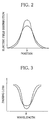
- FIG. 2 shows the electric field distribution of the light focusing on the end face 5b of the output-side slab waveguide in the optical multiplexer/demultiplexer A and that in the conventional optical multiplexer/demultiplexer each obtained by the simulation.
- the electric field distribution in the optical multiplexer/demultiplexer A of the present invention is shown with a solid line, and that in the conventional optical multiplexer/demultiplexer is shown with a broken line.
- the electric field distribution of the light on the slab waveguide end face 5b in the optical multiplexer/demultiplexer A of the present invention is more extended or broader in the direction of the width of the slab waveguide (the x2 direction) than that in the conventional optical multiplexer/demultiplexer.
- FIG. 3 shows the wavelength-dependent spectrum response of the optical multiplexer/demultiplexer A of the present invention and that of the conventional optical multiplexer/demultiplexer each obtained by the simulation.
- the wavelength-dependent spectrum response of the optical multiplexer/demultiplexer A of the present invention is shown with a solid line
- that of the conventional optical multiplexer/demultiplexer is shown with a broken line.
- the wavelength-dependency of the passing loss of the optical multiplexer/demultiplexer A of the present invention is reduced as compared with that of the conventional optical multiplexer/demultiplexer.
- the flatness of the wavelength-dependent spectrum response improves.
- an input waveguide 2 is connected to an input-side slab waveguide 3 through the medium of left and right narrow-width waveguides 7 and a wide-width waveguide portion 8.
- the left and right faces of a slab waveguide side end portion of the input waveguide 2 each obliquely extend outward as viewed in the direction of the width of the input waveguide 2, at an angle ⁇ relative to the optical axis (longitudinal axis) of the input waveguide 2.
- the slab waveguide side end portion of the input waveguide 2 has its width gradually increasing toward its end, that is, it is formed into an inverted tapered shape.
- sign W1 denotes the width of the remaining portion of the input waveguide 2
- sign 2B denotes the end face of the input waveguide 2, which extends perpendicularly to the optical axis of the input waveguide 2.
- the left and right narrow-width waveguides 7 are arranged apart from the input waveguide 2 by a distance g1 in the direction of the optical axis of the input waveguide 2, and apart from each other in the direction of the width of the input-side slab waveguide 3.
- the narrow-width waveguides 7 each obliquely extend relative to the optical axis of the input waveguide 2 at the same angle as the tapering angle ⁇ of the inverted tapered end portion of the input waveguide 2.
- the opposite end faces 7A, 7B of each narrow-width waveguide 7 are parallel to the end face 2B of the input waveguide 2.
- signs CW and SW denote distances between the two narrow-width waveguides 7 on the end face 7A side and the end face 7B side, respectively.
- the input-side slab waveguide 3 is arranged with its optical axis (longitudinal axis) aligned with the optical axis of the input waveguide 2, and a wide-width waveguide portion 8 is connected to the input-side slab waveguide 3 on its input waveguide 2 side.
- the wide-width waveguide portion 8 is arranged to face the narrow-width waveguides 7 with a distance g2 therebetween.
- the wide-width waveguide 8 is a trapezoidal shape whose length and width are H and W2, respectively.
- the left and right faces 8B of the wide-width waveguide portion 8 each obliquely extend relative to the optical axis of the input waveguide 2 and slab waveguide 3 at the same angle as the tapering angle ⁇ of the inverted tapered end portion of the input waveguide 2.
- the left face of the input waveguide 2, the outside face of the left narrow-width waveguide 7, and the left face of the wide-width waveguide portion 8 are on the same plane
- the right face of the input waveguide 2 the outside face of the right narrow-width waveguide 7, and the right face of the wide-width waveguide portion 8 are on the same plane.
- the optical multiplexer/demultiplexer A having the input waveguide 2 and the input-side slab waveguide 3 connected as shown in FIG. 4, light propagates through the input waveguide 2 and then enters a gap g1 from the end face 2B of the input waveguide 2. In the gap g1, since the light is released from confinement in the direction perpendicular to the optical axis of the input waveguide 2, the light is diffracted. The diffracted light enters the left and right narrow-width waveguides 7 from the gap g1 and propagates through the narrow-width waveguides 7.
- the electric field distribution of the light is of a bimodal shape having a deep depression at the central part of the distribution, as viewed in the direction perpendicular to the optical axis of the input waveguide 2.
- the light having an electric field distribution of such a bimodal shape, enters a gap g2 from the narrow-width waveguides 7. In the gap g2, since the light is released from confinement in the direction perpendicular to the optical axis of the input waveguide 2 and slab waveguide 3, the light is diffracted.
- the electric field distribution of the light, observed just before the light enters the wide-width waveguide portion 8 of the input-side slab waveguide 3 is of a bimodal shape, but the depression at its central part is a little less than that of the electric field distribution observed just after the light passes through the left and right narrow-width waveguides 7.
- the light having such electric field distribution then enters the wide-width waveguide portion 8 of the input-side slab waveguide 3.
- the wide-width waveguide portion 8 is made of a high refractive index layer. Therefore, as the light propagates through the wide-width waveguide portion 8, the depression observed at the center part of the bimodal electric field distribution of the light further decreases. In other words, in the electric field distribution of the light observed just before the light enters the input-side slab waveguide 3 from the wide-width waveguide portion 8, the difference between the minimum and maximum values decreases.
- the connecting structure shown in FIG. 4 the broadening of the electric field distribution of the light, observed just before the light enters the input-side slab waveguide 3, can be made larger.
- the light having such electric field distribution then propagates through the input-side slab waveguide 3, the arrayed waveguide grating 4 and the output-side slab waveguide 5 and focuses on the slab waveguide end face 5b.
- the broadening of the electric field distribution of the light focusing on the slab waveguide end face 5b is larger than that of the distribution observed just before the light enters the input-side slab waveguide 3.
- the broadening of the electric field distribution of the light is extended by virtue of the connecting structure shown in FIG. 4 before the light enters the input-side slab waveguide 3, and it is further extended by the output-side slab waveguide 5.
- the broadening of the electric field distribution of the light focusing on the output-side slab waveguide end face 5b becomes larger.
- the flatness of the wavelength-dependent spectrum response in a passing channel spacing is improved. Therefore, by connecting a plurality of input waveguides 2 to the input-side slab waveguide 3 as shown in FIG. 4, the flatness of the spectrum response in passing channel spacings can be improved.
- an output waveguide 6 has a relatively wide width W0 at its portion connected to a slab waveguide end face 5b.
- the slab waveguide side end portion of the output waveguide 6 is formed into a tapered shape whose left and right faces each obliquely extend inward relative to the optical axis at an angle ⁇ as viewed in the direction of the path width.
- an optical multiplexer/demultiplexer having the structure shown in FIG. 1 and adapted to multiplex a plurality of signal lightwaves having a frequency interval of 100GHz, that is, a wavelength interval of about 0.8nm in the 1.55 ⁇ m wavelength region and demultiplex a wavelength-multiplexed lightwave made of such signal lightwaves.
- a lower cladding layer including SiO 2 as a main ingredient
- a core layer including SiO 2 as a main ingredient and Ti as a dopant
- the core layer was dry-etched, and then, an upper cladding layer (including SiO 2 as a main ingredient) was formed by flame hydrosys deposition so that the dry-etched core layer was buried under it. Then, the upper cladding layer was converted into transparent glass by heating.
- the optical multiplexer/demultiplexer having specifications below was manufactured.
- a conventional optical multiplexer/demultiplexer was manufactured with the same specifications as those of the optical multiplexer/demultiplexer A, except that the focal lengths of the input-side and output-side slab waveguides were 8932 ⁇ m, each.
- the wavelength characteristic of the light emitted from the output waveguides was checked in the same manner as in the embodiment of the present invention. The result is shown with a broken line in FIG. 6.
- the 1dB passing wavelength band width (1dB channel spacing width) in the multiplexer/demultiplexer of the embodiment is 0.44nm, while that in the conventional multiplexer/demultiplexer is 0.24nm.
- the former is much larger than the latter.
- An optical multiplexer/demultiplexer according to embodiment 1 was manufactured using the connecting structure for connecting the input waveguide 2 and the input-side slab waveguide 3 as shown in FIG. 4 and the connecting structure for connecting the output-side slab waveguide 5 and the output waveguide 6 as shown in FIG. 5 with the specifications below.
- the wavelength characteristic of the emitted light in the optical multiplexer/demultiplexer was checked in the same manner as in embodiment 1. The result is shown in FIG. 7.
- the width of the 1dB passing wavelength band is 0.65nm, which is much larger than that in the conventional optical multiplexer/demultiplexer mentioned above.
- the present invention Is not restricted to the desirable mode and embodiments 1 and 2 described above. It can be modified in various manners.
- the optical multiplexer/demultiplexer A has, in the desirable mode described above, a plurality of input waveguides 2 and a plurality of output waveguides 6. However, it may have a single input waveguide 2 and a plurality of output waveguides 6. In that case, a wavelength-multiplexed lightwave is introduced through the single input waveguide 2 and separated into a plurality of signal lightwaves, and those signal lightwaves are taken out from the corresponding output waveguides 6, whereby the multiplexer function of the optical multiplexer/demultiplexer A is achieved.
- the optical multiplexer/demultiplexer may have a plurality of input waveguides 2 and a single output waveguide 6 in order to achieve the multiplexer and demultiplexer functions.
Landscapes
- Physics & Mathematics (AREA)
- Engineering & Computer Science (AREA)
- Microelectronics & Electronic Packaging (AREA)
- General Physics & Mathematics (AREA)
- Optics & Photonics (AREA)
- Optical Integrated Circuits (AREA)
Applications Claiming Priority (3)
| Application Number | Priority Date | Filing Date | Title |
|---|---|---|---|
| JP35044298 | 1998-12-09 | ||
| JP35044298A JP3615069B2 (ja) | 1998-12-09 | 1998-12-09 | アレイ導波路回折格子型光合分波器 |
| PCT/JP1999/006634 WO2000034811A1 (fr) | 1998-12-09 | 1999-11-29 | Multiplexeur et demultiplexeur a reseau de diffraction de guides d'ondes |
Publications (3)
| Publication Number | Publication Date |
|---|---|
| EP1059545A1 true EP1059545A1 (de) | 2000-12-13 |
| EP1059545A4 EP1059545A4 (de) | 2005-08-17 |
| EP1059545B1 EP1059545B1 (de) | 2006-05-24 |
Family
ID=18410534
Family Applications (1)
| Application Number | Title | Priority Date | Filing Date |
|---|---|---|---|
| EP99973331A Expired - Lifetime EP1059545B1 (de) | 1998-12-09 | 1999-11-29 | Multiplexer und demultiplexer basierend auf einem wellenleitergitter (awg) |
Country Status (5)
| Country | Link |
|---|---|
| US (1) | US6404946B1 (de) |
| EP (1) | EP1059545B1 (de) |
| JP (1) | JP3615069B2 (de) |
| DE (1) | DE69931471T2 (de) |
| WO (1) | WO2000034811A1 (de) |
Cited By (3)
| Publication number | Priority date | Publication date | Assignee | Title |
|---|---|---|---|---|
| GB2359682A (en) * | 1999-02-01 | 2001-08-29 | Samsung Electronics Co Ltd | Arrayed waveguide wavelength multiplexer-demultiplexer with uniform loss |
| WO2002088791A3 (en) * | 2001-04-25 | 2003-03-13 | Lightwave Microsystems Corp | Multimode interference coupler for wdm applications |
| EP2015117A1 (de) * | 2007-07-13 | 2009-01-14 | Enablence USA Components Inc. | Ultrabreitband-AWG-Multiplexer |
Families Citing this family (14)
| Publication number | Priority date | Publication date | Assignee | Title |
|---|---|---|---|---|
| US6473546B2 (en) * | 2000-07-28 | 2002-10-29 | Sumitomo Electric Industries, Ltd. | Optical multiplexer/demultiplexer |
| JP3687529B2 (ja) * | 2000-11-16 | 2005-08-24 | 日本電気株式会社 | アレイ導波路格子、光送信装置および光通信システム |
| US6823103B2 (en) * | 2000-12-15 | 2004-11-23 | Lightwave Microsystems Corporation | Optical devices for controlling insertion loss |
| CA2328696C (en) * | 2000-12-18 | 2008-08-12 | Jds Uniphase Inc. | Periodic arrayed waveguide grating multiplexer/demultiplexer |
| JP2003075666A (ja) * | 2001-06-22 | 2003-03-12 | Furukawa Electric Co Ltd:The | アレイ導波路回折格子型光合分波器 |
| US7509048B2 (en) * | 2001-07-20 | 2009-03-24 | Essex Corporation | Method and apparatus for optical signal processing using an optical tapped delay line |
| US7006719B2 (en) * | 2002-03-08 | 2006-02-28 | Infinera Corporation | In-wafer testing of integrated optical components in photonic integrated circuits (PICs) |
| KR100594041B1 (ko) | 2004-01-19 | 2006-06-30 | 삼성전자주식회사 | 비대칭 도파로열 격자 |
| US7792403B1 (en) | 2005-09-08 | 2010-09-07 | Infinera Corporation | Adiabatic polarization converter |
| US20090016725A1 (en) * | 2007-06-29 | 2009-01-15 | Schlumberger Technology Corporation | Wavelengths multiplexer method and apparatus for optical logging tools |
| US7565041B2 (en) * | 2007-10-26 | 2009-07-21 | Infinera Corporation | Symmetric optical circuit with integrated polarization rotator |
| JP2009206757A (ja) * | 2008-02-27 | 2009-09-10 | Fujitsu Ltd | 光回路 |
| EP2401640A4 (de) * | 2009-02-26 | 2014-04-16 | Aidi Corp | Arrayed-waveguide-grating (awg) mit verschiedenen radii in den eingangs- und ausgangsplattenbereichen |
| CN107735707B (zh) | 2015-03-20 | 2023-05-02 | 拉瓦尔大学 | 用于调谐光学信号的光学装置和方法 |
Family Cites Families (7)
| Publication number | Priority date | Publication date | Assignee | Title |
|---|---|---|---|---|
| JP2599786B2 (ja) * | 1989-03-17 | 1997-04-16 | 日本電信電話株式会社 | 導波路形回折格子 |
| US5412744A (en) * | 1994-05-02 | 1995-05-02 | At&T Corp. | Frequency routing device having a wide and substantially flat passband |
| JPH08122557A (ja) * | 1994-10-20 | 1996-05-17 | Hitachi Cable Ltd | 光波長合分波器 |
| US5706377A (en) | 1996-07-17 | 1998-01-06 | Lucent Technologies Inc. | Wavelength routing device having wide and flat passbands |
| JPH112733A (ja) | 1997-06-13 | 1999-01-06 | Nippon Telegr & Teleph Corp <Ntt> | アレイ格子型光合分波器 |
| JP3029028B2 (ja) * | 1997-11-26 | 2000-04-04 | 日立電線株式会社 | 光波長合分波器 |
| US6069990A (en) * | 1997-11-27 | 2000-05-30 | Hitachi Cable Ltd. | Optical wavelength multiplexer/demultiplexer |
-
1998
- 1998-12-09 JP JP35044298A patent/JP3615069B2/ja not_active Expired - Fee Related
-
1999
- 1999-11-29 WO PCT/JP1999/006634 patent/WO2000034811A1/ja not_active Ceased
- 1999-11-29 EP EP99973331A patent/EP1059545B1/de not_active Expired - Lifetime
- 1999-11-29 DE DE69931471T patent/DE69931471T2/de not_active Expired - Fee Related
-
2000
- 2000-08-09 US US09/635,492 patent/US6404946B1/en not_active Expired - Fee Related
Non-Patent Citations (2)
| Title |
|---|
| No further relevant documents disclosed * |
| See also references of WO0034811A1 * |
Cited By (7)
| Publication number | Priority date | Publication date | Assignee | Title |
|---|---|---|---|---|
| GB2359682A (en) * | 1999-02-01 | 2001-08-29 | Samsung Electronics Co Ltd | Arrayed waveguide wavelength multiplexer-demultiplexer with uniform loss |
| GB2359682B (en) * | 1999-02-01 | 2002-03-20 | Samsung Electronics Co Ltd | Optical wavelength multiplexer/demultiplexer with uniform loss |
| US6442308B1 (en) | 1999-02-01 | 2002-08-27 | Dong-Kyoon Han | Optical wavelength multiplexer/demultiplexer with uniform loss |
| WO2002088791A3 (en) * | 2001-04-25 | 2003-03-13 | Lightwave Microsystems Corp | Multimode interference coupler for wdm applications |
| US6563988B2 (en) | 2001-04-25 | 2003-05-13 | Lightwave Microsystems Corporation | Optical apparatus and method having predetermined group velocity dispersion |
| EP2015117A1 (de) * | 2007-07-13 | 2009-01-14 | Enablence USA Components Inc. | Ultrabreitband-AWG-Multiplexer |
| US7840104B2 (en) | 2007-07-13 | 2010-11-23 | Enablence USA Components, Inc. | Ultra-wide band AWG multiplexer |
Also Published As
| Publication number | Publication date |
|---|---|
| US6404946B1 (en) | 2002-06-11 |
| EP1059545A4 (de) | 2005-08-17 |
| DE69931471D1 (de) | 2006-06-29 |
| WO2000034811A1 (fr) | 2000-06-15 |
| DE69931471T2 (de) | 2006-09-28 |
| JP3615069B2 (ja) | 2005-01-26 |
| JP2000171661A (ja) | 2000-06-23 |
| EP1059545B1 (de) | 2006-05-24 |
Similar Documents
| Publication | Publication Date | Title |
|---|---|---|
| US6069990A (en) | Optical wavelength multiplexer/demultiplexer | |
| CA2198836C (en) | Optical wavelength multiplexer/demultiplexer | |
| EP1059545B1 (de) | Multiplexer und demultiplexer basierend auf einem wellenleitergitter (awg) | |
| US10495813B2 (en) | Echelle grating multiplexer or demultiplexer | |
| EP1226461B1 (de) | Phasar mit flacher durchlasskurve | |
| US5982960A (en) | Optical wavelength multiplexer/demultiplexer | |
| US5581639A (en) | Raman-nath diffraction grating | |
| WO2000011508A1 (en) | Array waveguide diffraction grating optical multiplexer/demultiplexer | |
| JP3139571B2 (ja) | 光合分波器 | |
| US6567587B2 (en) | Dispersion compensator and dispersion-compensating module employing the same | |
| JP3039491B2 (ja) | 光波長合分波器 | |
| EP1373950B1 (de) | Phasengesteuertes wellenleitergitter | |
| US7043120B2 (en) | Array waveguide grating | |
| US6741772B2 (en) | Optical multiplexer/demultiplexer and waveguide type optical coupler | |
| US6798952B2 (en) | Optical multiplexer/demultiplexer | |
| JP3625666B2 (ja) | 光波長合分波器 | |
| KR100594040B1 (ko) | 듀얼 밴드 파장분할 다중화기 | |
| JP2861996B1 (ja) | 光波長合分波器 | |
| JP3029028B2 (ja) | 光波長合分波器 | |
| JP2003066269A (ja) | 波長多重分離光学デバイス及び波長多重光伝送モジュール | |
| JP4123519B2 (ja) | 光導波路及び光合分波器 | |
| JPH0973018A (ja) | 光波長合分波器 | |
| JP4284852B2 (ja) | 光合分波器 | |
| US20030086650A1 (en) | Arrayed waveguide grating type optical multiplexer/demultiplexer | |
| JP2001091765A (ja) | アレイ導波路回折格子型光合分波器 |
Legal Events
| Date | Code | Title | Description |
|---|---|---|---|
| PUAI | Public reference made under article 153(3) epc to a published international application that has entered the european phase |
Free format text: ORIGINAL CODE: 0009012 |
|
| 17P | Request for examination filed |
Effective date: 20000814 |
|
| AK | Designated contracting states |
Kind code of ref document: A1 Designated state(s): AT BE CH CY DE DK ES FI FR GB GR IE IT LI LU MC NL PT SE |
|
| AX | Request for extension of the european patent |
Free format text: AL;LT;LV;MK;RO;SI |
|
| RBV | Designated contracting states (corrected) |
Designated state(s): DE FR GB |
|
| A4 | Supplementary search report drawn up and despatched |
Effective date: 20050701 |
|
| GRAP | Despatch of communication of intention to grant a patent |
Free format text: ORIGINAL CODE: EPIDOSNIGR1 |
|
| GRAS | Grant fee paid |
Free format text: ORIGINAL CODE: EPIDOSNIGR3 |
|
| GRAA | (expected) grant |
Free format text: ORIGINAL CODE: 0009210 |
|
| AK | Designated contracting states |
Kind code of ref document: B1 Designated state(s): DE FR GB |
|
| REG | Reference to a national code |
Ref country code: GB Ref legal event code: FG4D |
|
| REF | Corresponds to: |
Ref document number: 69931471 Country of ref document: DE Date of ref document: 20060629 Kind code of ref document: P |
|
| ET | Fr: translation filed | ||
| PLBE | No opposition filed within time limit |
Free format text: ORIGINAL CODE: 0009261 |
|
| STAA | Information on the status of an ep patent application or granted ep patent |
Free format text: STATUS: NO OPPOSITION FILED WITHIN TIME LIMIT |
|
| 26N | No opposition filed |
Effective date: 20070227 |
|
| PGFP | Annual fee paid to national office [announced via postgrant information from national office to epo] |
Ref country code: DE Payment date: 20081127 Year of fee payment: 10 |
|
| PGFP | Annual fee paid to national office [announced via postgrant information from national office to epo] |
Ref country code: FR Payment date: 20081112 Year of fee payment: 10 |
|
| REG | Reference to a national code |
Ref country code: FR Ref legal event code: ST Effective date: 20100730 |
|
| PG25 | Lapsed in a contracting state [announced via postgrant information from national office to epo] |
Ref country code: FR Free format text: LAPSE BECAUSE OF NON-PAYMENT OF DUE FEES Effective date: 20091130 |
|
| PG25 | Lapsed in a contracting state [announced via postgrant information from national office to epo] |
Ref country code: DE Free format text: LAPSE BECAUSE OF NON-PAYMENT OF DUE FEES Effective date: 20100601 |
|
| PGFP | Annual fee paid to national office [announced via postgrant information from national office to epo] |
Ref country code: GB Payment date: 20131127 Year of fee payment: 15 |
|
| GBPC | Gb: european patent ceased through non-payment of renewal fee |
Effective date: 20141129 |
|
| PG25 | Lapsed in a contracting state [announced via postgrant information from national office to epo] |
Ref country code: GB Free format text: LAPSE BECAUSE OF NON-PAYMENT OF DUE FEES Effective date: 20141129 |