EP1059701A2 - Dispositif de codage - Google Patents
Dispositif de codage Download PDFInfo
- Publication number
- EP1059701A2 EP1059701A2 EP00109488A EP00109488A EP1059701A2 EP 1059701 A2 EP1059701 A2 EP 1059701A2 EP 00109488 A EP00109488 A EP 00109488A EP 00109488 A EP00109488 A EP 00109488A EP 1059701 A2 EP1059701 A2 EP 1059701A2
- Authority
- EP
- European Patent Office
- Prior art keywords
- coding
- elements
- parts
- module
- circuit board
- Prior art date
- Legal status (The legal status is an assumption and is not a legal conclusion. Google has not performed a legal analysis and makes no representation as to the accuracy of the status listed.)
- Granted
Links
Images





Classifications
-
- H—ELECTRICITY
- H01—ELECTRIC ELEMENTS
- H01R—ELECTRICALLY-CONDUCTIVE CONNECTIONS; STRUCTURAL ASSOCIATIONS OF A PLURALITY OF MUTUALLY-INSULATED ELECTRICAL CONNECTING ELEMENTS; COUPLING DEVICES; CURRENT COLLECTORS
- H01R13/00—Details of coupling devices of the kinds covered by groups H01R12/70 or H01R24/00 - H01R33/00
- H01R13/64—Means for preventing incorrect coupling
- H01R13/645—Means for preventing incorrect coupling by exchangeable elements on case or base
- H01R13/6456—Means for preventing incorrect coupling by exchangeable elements on case or base comprising keying elements at different positions along the periphery of the connector
-
- H—ELECTRICITY
- H05—ELECTRIC TECHNIQUES NOT OTHERWISE PROVIDED FOR
- H05K—PRINTED CIRCUITS; CASINGS OR CONSTRUCTIONAL DETAILS OF ELECTRIC APPARATUS; MANUFACTURE OF ASSEMBLAGES OF ELECTRICAL COMPONENTS
- H05K7/00—Constructional details common to different types of electric apparatus
- H05K7/14—Mounting supporting structure in casing or on frame or rack
- H05K7/1438—Back panels or connecting means therefor; Terminals; Coding means to avoid wrong insertion
- H05K7/1452—Mounting of connectors; Switching; Reinforcing of back panels
- H05K7/1455—Coding for prevention of wrong insertion
Definitions
- the invention relates to a coding device for mechanically assembled Parts, in particular circuit board connectors, the ones to be connected Parts are each provided with at least one coding element, and a method for coding two mechanically joinable Divide.
- a coding of mechanically joinable parts e.g. Connectors is required to make a distinctive exchange or exchange to be able to make these parts and to ensure the functionality of the units connected to these parts, e.g. electrical controls on printed circuit boards, ensure.
- Printed circuit board connectors with mechanical coding devices are known equip to confuse different circuit boards to prevent. Pins, discs or other molded parts, so in corresponding recesses inside or outside a connector inserted or attached that the insertion of an incorrectly coded Plug connection is prevented.
- the known coding devices are problematic with the increasing Miniaturization of the connectors, since the corresponding coding devices have to be made smaller and more difficult, the coding devices partially inserted with a special tool and have to be removed again.
- This invention is therefore based on the object of a coding device for coding mechanically connectable parts of the aforementioned Form in such a way that with a simple and tool-free assembly the connection is securely coded.
- This object is achieved in that two belonging together Coding elements are designed as a one-piece coding module, the Coding elements are held together by means of web-like connections.
- the coding device for coding mechanically connectable parts such as, for example, printed circuit board connectors
- the plug connection is put together, by means of a fastening means on the coding device, to the other PCB is pressed on.
- the webs break, with which the two coding elements are held together to form a coding module, and the connection can be released again and coded at the same time.
- the advantage here is that no special tool is required for this process.
- Another advantage is that due to the solid and stable design of the coding modules, which can be chosen in any shape and color, no mechanical destruction of the coding elements is to be expected during a plug-in process.
- Another advantage is that incorrect coding of the connectors, those in a separate or independent production of related Printed circuit boards can be avoided because the final Completion of such devices equipped with coded connectors, the final assembly was carried out by appropriately experienced experts where a misplacement can be largely excluded.
- the coding module is first attached to one of the connectable parts and during the assembly process with the other part, automatically connected to it with the merging process, the two at the same time Coding elements are separated so that the assembled parts are now can be separated again in coded version.
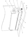
- the coding module 1 in FIG. 4 is designed, for example, as a cuboid block and consists of two parts, the coding elements 2 and 3, which are connected to one another by web-like connections 4.
- the coding elements are kept at a uniform distance or separated from one another by a gap 9, the orientation of the web-like connections 4 preferably being perpendicular to the direction of insertion. If a pressure force is exerted on the coding elements in the plug-in direction until the coding elements initially spaced apart by the gap 9 break, the web-like connections 4 break and the coding module 1 is divided into two individual coding elements 2 and 3.
- a projection 7 is formed on one side, approximately centrally to the total height of the coding module, on which a guide element 6 is arranged.
- this guide element 6 protrudes into a corresponding recess 14 in a printed circuit board connector 12 and is used first of all to preassemble the coding module 1 and the printed circuit board connector 12 before the coding module with the coding element 2 is fastened through a hole by means of a fastening means 18 5 is attached to a circuit board 10. (see also Fig. 10)
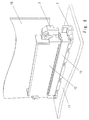
- two coding modules 1 are fastened to the printed circuit board 10 on both sides of a printed circuit board connector 12. If the plug connectors 12, 13 of the printed circuit boards 10, 11 are plugged together, the pin 15 is permanently pressed into the corresponding bore 8 in the coding element 3.
- the web-like connections 4 between the two coding elements are stretched by the compressive forces that occur until they break and the two coding elements are firmly joined together are.
- the connection of the associated coding elements 2, 3 is thus separated and an automatic coding of the plug connection has occurred.
- the plug connection between the printed circuit board 10 and the printed circuit board 11 can be released again immediately if required, the coding only permitting a connection of printed circuit boards in this combination of plug connector and coding element.
- FIG. 9 shows a variant of the assembly of the coding modules described above. It is provided here that a correspondingly arranged bore 17 is provided in the printed circuit board 11, so that a press-in pin 16 which is firmly embedded or also molded into the coding element 3 of the coding module 1 can be pressed into the bore 17.
- the coding module 1 is first also fixed on the printed circuit board 10 by means of the fastening means 18 and the plug connectors 12, 13 of the printed circuit boards 10, 11 are inserted into one another.
- the assembled press-in pin 16 presses permanently into the bore 17 provided in the printed circuit board 11, the web-like connections 4 break and release the connection between the coding elements 2 and 3.
- FIG. 10 shows a circuit board connector 12 and a coding module 1 in a detailed drawing before assembly on a circuit board 10.
- the guide element 6 on the projection 7 can be clearly seen, which hooks into the recess 14 on the printed circuit board connector 12 and results in a secure and stable connection by means of a fastening means 18, not shown here, through the bore 5 of the coding element 2 to the printed circuit board 10.
- a method for coding two mechanically joinable parts 10, 11 is described below, wherein a coding module 1 consisting of two coding elements 2, 3 and held together with web-like connections 4 is connected to the parts 10, 11.
- the coding element 2 is attached to the first part 10.
- the parts 10 and 11 are then joined together, the coding element 3 being simultaneously fixed on the second part 11 with the fastening means 15.
- the coding elements 2, 3, which are spaced apart by the webs 4 are pressed against one another, so that the webs are sheared off and break, and at the same time the coding element 3 is permanently attached to the second part by means of the fastening means 15 11 attached. This creates a detachable and coded connection between the first and second parts 10, 11, the second part 11 remaining connected to the coding element 3 and the first part 10 being connected to the coding element 2.
Landscapes
- Engineering & Computer Science (AREA)
- Microelectronics & Electronic Packaging (AREA)
- Combinations Of Printed Boards (AREA)
- Connection Of Plates (AREA)
- Coupling Device And Connection With Printed Circuit (AREA)
Applications Claiming Priority (2)
| Application Number | Priority Date | Filing Date | Title |
|---|---|---|---|
| DE19925347 | 1999-06-02 | ||
| DE19925347A DE19925347A1 (de) | 1999-06-02 | 1999-06-02 | Kodiereinrichtung |
Publications (3)
| Publication Number | Publication Date |
|---|---|
| EP1059701A2 true EP1059701A2 (fr) | 2000-12-13 |
| EP1059701A3 EP1059701A3 (fr) | 2002-07-17 |
| EP1059701B1 EP1059701B1 (fr) | 2005-10-26 |
Family
ID=7910066
Family Applications (1)
| Application Number | Title | Priority Date | Filing Date |
|---|---|---|---|
| EP00109488A Expired - Lifetime EP1059701B1 (fr) | 1999-06-02 | 2000-05-04 | Dispositif de codage |
Country Status (3)
| Country | Link |
|---|---|
| US (1) | US6203380B1 (fr) |
| EP (1) | EP1059701B1 (fr) |
| DE (2) | DE19925347A1 (fr) |
Families Citing this family (7)
| Publication number | Priority date | Publication date | Assignee | Title |
|---|---|---|---|---|
| US6435897B1 (en) * | 2000-04-10 | 2002-08-20 | Storcase Technology, Inc. | Compact PCI connector guide |
| US6533587B1 (en) * | 2000-07-05 | 2003-03-18 | Network Engines, Inc. | Circuit board riser |
| TW532604U (en) * | 2002-04-19 | 2003-05-11 | Giga Byte Tech Co Ltd | Improved structure of computer bus cable connecting seat |
| DE20214863U1 (de) * | 2002-09-26 | 2004-02-19 | Weidmüller Interface Gmbh & Co. | Vorrichtung zur Montage eines Anschlußelementes an einem Bauelement |
| DE202007002248U1 (de) * | 2007-02-15 | 2007-06-06 | Harting Electric Gmbh & Co. Kg | Kodiereinrichtung für Steckverbinder |
| DE102008009350A1 (de) | 2008-02-14 | 2009-08-20 | Weidmüller Interface GmbH & Co. KG | Steckverbindung mit einer Kodiervorrichtung und Verfahren zur Montage der Kodiervorrichtung an der Steckverbindung |
| DE202022106490U1 (de) * | 2022-11-21 | 2024-02-27 | WAGO Verwaltungsgesellschaft mit beschränkter Haftung | Kodierbauteil und Kodierelement sowie Set aus Steckverbinder und Kodierbauteil |
Family Cites Families (9)
| Publication number | Priority date | Publication date | Assignee | Title |
|---|---|---|---|---|
| DE8428477U1 (de) * | 1984-09-27 | 1986-02-27 | Siemens AG, 1000 Berlin und 8000 München | Mehrpolige elektrische Steckverbindung mit einer Codiereinrichtung |
| NO855307L (no) * | 1985-03-28 | 1986-09-29 | Siemens Ag | Kodeanordning for byggegrupper som kan skyves inn i en byggegrupperamme. |
| US5030141A (en) * | 1990-06-28 | 1991-07-09 | Hughes Aircraft Company | Key connector |
| US5096443A (en) * | 1990-11-29 | 1992-03-17 | Siemens Aktiengesellschaft | Keyed apparatus for providing ground, power or signal connections |
| DE9208701U1 (de) | 1992-06-29 | 1992-12-17 | Siemens AG, 8000 München | Codiereinrichtung für elektrische Baugruppen |
| US5346412A (en) * | 1993-07-27 | 1994-09-13 | The Whitaker Corporation | Break away key and latch assembly |
| GB9400023D0 (en) * | 1994-01-04 | 1994-03-02 | Amp Gmbh | Keying comb for connectors |
| US5769668A (en) * | 1996-03-08 | 1998-06-23 | Robinson Nugent, Inc. | Module alignment apparatus for an electrical connector |
| DE29906583U1 (de) * | 1999-04-14 | 1999-07-15 | Weidmüller Interface GmbH & Co., 32758 Detmold | Kodiervorrichtung zur Kodierung eines elektrischen Gerätes |
-
1999
- 1999-06-02 DE DE19925347A patent/DE19925347A1/de not_active Withdrawn
-
2000
- 2000-05-04 EP EP00109488A patent/EP1059701B1/fr not_active Expired - Lifetime
- 2000-05-04 DE DE50011413T patent/DE50011413D1/de not_active Expired - Lifetime
- 2000-06-01 US US09/586,707 patent/US6203380B1/en not_active Expired - Lifetime
Also Published As
| Publication number | Publication date |
|---|---|
| EP1059701A3 (fr) | 2002-07-17 |
| DE50011413D1 (de) | 2005-12-01 |
| US6203380B1 (en) | 2001-03-20 |
| DE19925347A1 (de) | 2000-12-07 |
| EP1059701B1 (fr) | 2005-10-26 |
Similar Documents
| Publication | Publication Date | Title |
|---|---|---|
| DE3810471C2 (fr) | ||
| DE3437988C2 (fr) | ||
| DE69709987T2 (de) | Verbinder für Leiterplatte | |
| DE69630334T2 (de) | Steckverbinder für gedruckte Schaltung | |
| DE102007037839A1 (de) | Zweiendiger Einpreßverbinder | |
| DE102014106277B4 (de) | Ein Elektronikgehäuse mit einer Anschlussleiste für ein Elektronikgerät | |
| DE102020127203B4 (de) | Steckverbinderanordnung | |
| EP0867342B1 (fr) | Centrale de distribution électrique pour véhicule automobile et procédé pour sa fabrication | |
| EP0397057B1 (fr) | Assemblage pour la connexion mécanique et électrique d'une plaque de câblage d'extension à une plaque de câblage de base | |
| DE3401428A1 (de) | Einrichtung zur loesbaren verbindung einer schaltungsplatte | |
| EP1191643A2 (fr) | Boítier pour un dispositif électronique | |
| EP0846351B1 (fr) | Dispositif constitue de deux demi-fiches pour fixation dans une paroi | |
| DE3116410C2 (fr) | ||
| EP1059701B1 (fr) | Dispositif de codage | |
| DE60118687T2 (de) | Verbinder zur Befestigung auf eine Leiterplatte und Anordnung zur Befestigung eines Verbinders auf eine Leiterplatte | |
| WO1991011041A1 (fr) | Connecteur rectiligne | |
| DE4218431A1 (de) | Einrichtung zur Verbindung eines Steckverbinders mit einer Leiterplatte | |
| DE2937883C2 (de) | Anschlußstift für lötfreie Anschlußtechniken | |
| DE3806049C2 (fr) | ||
| DE10243313B4 (de) | Kodierbarer Steckverbinder | |
| DE3625865C2 (fr) | ||
| DE102016212258A1 (de) | Kombination, umfassend einen Stecker und eine Fädelhilfe, Fädelhilfe, Anordnung und Verfahren zum Anbringen eines Steckers an einer Leiterplatte | |
| DE19528074A1 (de) | Elektrische Steckeranordnung | |
| DE19610610A1 (de) | Anordnung zur Verbindung eines elektrischen Leiters mit einem Schneidklemmkontakt | |
| DE102020132630A1 (de) | Umspritzte Kontaktanordnung |
Legal Events
| Date | Code | Title | Description |
|---|---|---|---|
| PUAI | Public reference made under article 153(3) epc to a published international application that has entered the european phase |
Free format text: ORIGINAL CODE: 0009012 |
|
| AK | Designated contracting states |
Kind code of ref document: A2 Designated state(s): AT BE CH CY DE DK ES FI FR GB GR IE IT LI LU MC NL PT SE |
|
| AX | Request for extension of the european patent |
Free format text: AL;LT;LV;MK;RO;SI |
|
| PUAL | Search report despatched |
Free format text: ORIGINAL CODE: 0009013 |
|
| AK | Designated contracting states |
Kind code of ref document: A3 Designated state(s): AT BE CH CY DE DK ES FI FR GB GR IE IT LI LU MC NL PT SE |
|
| AX | Request for extension of the european patent |
Free format text: AL;LT;LV;MK;RO;SI |
|
| 17P | Request for examination filed |
Effective date: 20020923 |
|
| AKX | Designation fees paid |
Designated state(s): DE FI FR GB |
|
| RBV | Designated contracting states (corrected) |
Designated state(s): DE FR GB IT |
|
| RAP1 | Party data changed (applicant data changed or rights of an application transferred) |
Owner name: HARTING ELECTRONICS GMBH & CO. KG |
|
| GRAP | Despatch of communication of intention to grant a patent |
Free format text: ORIGINAL CODE: EPIDOSNIGR1 |
|
| GRAS | Grant fee paid |
Free format text: ORIGINAL CODE: EPIDOSNIGR3 |
|
| GRAA | (expected) grant |
Free format text: ORIGINAL CODE: 0009210 |
|
| AK | Designated contracting states |
Kind code of ref document: B1 Designated state(s): DE FR GB IT |
|
| REG | Reference to a national code |
Ref country code: GB Ref legal event code: FG4D Free format text: NOT ENGLISH |
|
| REF | Corresponds to: |
Ref document number: 50011413 Country of ref document: DE Date of ref document: 20051201 Kind code of ref document: P |
|
| GBT | Gb: translation of ep patent filed (gb section 77(6)(a)/1977) |
Effective date: 20060108 |
|
| ET | Fr: translation filed | ||
| PLBE | No opposition filed within time limit |
Free format text: ORIGINAL CODE: 0009261 |
|
| STAA | Information on the status of an ep patent application or granted ep patent |
Free format text: STATUS: NO OPPOSITION FILED WITHIN TIME LIMIT |
|
| 26N | No opposition filed |
Effective date: 20060727 |
|
| PGFP | Annual fee paid to national office [announced via postgrant information from national office to epo] |
Ref country code: GB Payment date: 20110525 Year of fee payment: 12 |
|
| PGFP | Annual fee paid to national office [announced via postgrant information from national office to epo] |
Ref country code: IT Payment date: 20110523 Year of fee payment: 12 |
|
| GBPC | Gb: european patent ceased through non-payment of renewal fee |
Effective date: 20120504 |
|
| PG25 | Lapsed in a contracting state [announced via postgrant information from national office to epo] |
Ref country code: IT Free format text: LAPSE BECAUSE OF NON-PAYMENT OF DUE FEES Effective date: 20120504 |
|
| PG25 | Lapsed in a contracting state [announced via postgrant information from national office to epo] |
Ref country code: GB Free format text: LAPSE BECAUSE OF NON-PAYMENT OF DUE FEES Effective date: 20120504 |
|
| REG | Reference to a national code |
Ref country code: FR Ref legal event code: PLFP Year of fee payment: 17 |
|
| PGFP | Annual fee paid to national office [announced via postgrant information from national office to epo] |
Ref country code: DE Payment date: 20160426 Year of fee payment: 17 |
|
| PGFP | Annual fee paid to national office [announced via postgrant information from national office to epo] |
Ref country code: FR Payment date: 20160412 Year of fee payment: 17 |
|
| REG | Reference to a national code |
Ref country code: DE Ref legal event code: R119 Ref document number: 50011413 Country of ref document: DE |
|
| REG | Reference to a national code |
Ref country code: FR Ref legal event code: ST Effective date: 20180131 |
|
| PG25 | Lapsed in a contracting state [announced via postgrant information from national office to epo] |
Ref country code: DE Free format text: LAPSE BECAUSE OF NON-PAYMENT OF DUE FEES Effective date: 20171201 |
|
| PG25 | Lapsed in a contracting state [announced via postgrant information from national office to epo] |
Ref country code: FR Free format text: LAPSE BECAUSE OF NON-PAYMENT OF DUE FEES Effective date: 20170531 |