EP1060574B1 - Differentieller leitungstreiber - Google Patents
Differentieller leitungstreiber Download PDFInfo
- Publication number
- EP1060574B1 EP1060574B1 EP99908046A EP99908046A EP1060574B1 EP 1060574 B1 EP1060574 B1 EP 1060574B1 EP 99908046 A EP99908046 A EP 99908046A EP 99908046 A EP99908046 A EP 99908046A EP 1060574 B1 EP1060574 B1 EP 1060574B1
- Authority
- EP
- European Patent Office
- Prior art keywords
- nmos transistor
- current
- input
- output
- gate
- Prior art date
- Legal status (The legal status is an assumption and is not a legal conclusion. Google has not performed a legal analysis and makes no representation as to the accuracy of the status listed.)
- Expired - Lifetime
Links
- RYGMFSIKBFXOCR-UHFFFAOYSA-N Copper Chemical compound [Cu] RYGMFSIKBFXOCR-UHFFFAOYSA-N 0.000 claims description 9
- 229910052802 copper Inorganic materials 0.000 claims description 8
- 239000010949 copper Substances 0.000 claims description 8
- 238000004804 winding Methods 0.000 claims description 5
- 238000000034 method Methods 0.000 description 5
- 230000001419 dependent effect Effects 0.000 description 2
- 230000005540 biological transmission Effects 0.000 description 1
- 230000015556 catabolic process Effects 0.000 description 1
- 238000010276 construction Methods 0.000 description 1
- 230000007423 decrease Effects 0.000 description 1
- 229920005994 diacetyl cellulose Polymers 0.000 description 1
- 230000000694 effects Effects 0.000 description 1
- 238000004519 manufacturing process Methods 0.000 description 1
- 230000003071 parasitic effect Effects 0.000 description 1
Images

Classifications
-
- H—ELECTRICITY
- H03—ELECTRONIC CIRCUITRY
- H03M—CODING; DECODING; CODE CONVERSION IN GENERAL
- H03M1/00—Analogue/digital conversion; Digital/analogue conversion
- H03M1/66—Digital/analogue converters
- H03M1/74—Simultaneous conversion
- H03M1/80—Simultaneous conversion using weighted impedances
-
- H—ELECTRICITY
- H04—ELECTRIC COMMUNICATION TECHNIQUE
- H04L—TRANSMISSION OF DIGITAL INFORMATION, e.g. TELEGRAPHIC COMMUNICATION
- H04L25/00—Baseband systems
- H04L25/02—Details ; arrangements for supplying electrical power along data transmission lines
- H04L25/0264—Arrangements for coupling to transmission lines
- H04L25/0266—Arrangements for providing Galvanic isolation, e.g. by means of magnetic or capacitive coupling
Definitions
- the invention regards a CMOS differential line driver, in particular for driving a line comprising a twisted copper pair, and having a differential input with two input terminals and a differential analog output with two output terminals, which are each provided with a terminal resistor. It is thought primarily for use with twisted copper pairs or the like as used for high speed applications like high speed internet access.
- FIG. 1 A traditional type of a fully differential line driver is shown schematically in Fig. 1.
- the twisted copper pair I is fed with power via a transformer 2.
- the transformed impedance of the twisted copper pair must be matched by termination resistors R ⁇ .
- the line driver must have a low output impedance and high common-mode rejection, since very high voltage in the copper wire may be coupled back as common-mode signals via parasitic capacitance.
- the input dependent variation in the output impedance of the line driver must also be very small in order to have low distortion. Therefore, effective feedbacks are needed in the line driver. Improper compensation in the line driver may result in low signal bandwidth and/or instability.
- US 5,166,635 describes a differential line driver architecture that comprises a first stage having a fully differential folded cascode amplifier and a second stage having a push-pull CMOS output with complimentary error amplifier feedback.
- the first stage provides the majority of the open loop gain and uses a sole common mode feedback circuit.
- the second stage uses complimentary error amplifier feedback and produces near unity gain for reducing distortion and providing low output impedance.
- the use of feedback may lead to potential operational instability under some conditions that are undesirable for use with some applications.
- a line driver of the envisaged type would usually be handling signals from a high speed digital-to-analog converter (DAC) for high speed internet access. It is normal for such high speed DACs to be arranged as current output devices, meaning that the driving DAC would have a high output impedance. In order to minimize the distortion in the DAC, the input impedance of the line driver must be low.
- DAC digital-to-analog converter
- amplifying circuits are used, which are current amplifying, enabling the obtaining of a low input impedance and a high output impedance.
- termination resistors are arranged.
- a line driver is provided with a pair of current inputs I inp and I inn .
- the line driver (inside the dashed rectangle) has a pair of current outputs, which are provided with terminal resistors R t connected to drive voltages V ddh and connected to a transformer winding, with another winding connected to a twisted copper pair.
- R t terminal resistors
- the line driver itself will have a very low input impedance. Unlike the traditional approach shown in Fig. 1, the proposed line driver has a very high output impedance. Having a low input impedance and a high output impedance, this line driver thus is a current-mode line driver. The termination resistors at the outputs of the line drivers will give high common-mode rejection and impedance matching.
- the outputs of the DAC i.e. the input currents to the line driver
- I i n p I o s + i ac / 2
- I i n n I o s ⁇ i ac / 2
- I os is constant
- i ac is the analog representation of the digital input signal of the DAC.
- I o n A ⁇ ( I o s ⁇ i ac / 2 )
- the use of an extra supply voltage for the termination resistors is advantageous in that large common-mode signals are directed to this extra supply voltage without disturbing the supply voltages for the DAC and current amplifiers.
- a disadvantage would be the power efficiency, since some power is wasted on the termination resistors due to the matching requirement.
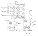
- Fig. 3 is shown an example for a current amplifier, forming one of the amplifiers A P within the dashed rectangle in Fig. 2.
- the amplifier A n may be rigorously similar, only the first-mentioned current amplifier is shown in Fig. 2, with inputs and outputs shown.
- NMOS transistors In order to have high signal bandwidth, it is preferable to use only NMOS transistors in the signal path. For obtaining a large gain A, it is preferable to use several stages in cascade in order to maintain the high bandwidth.
- the current amplifier consists of two stages, The first stage comprises transistors M1, M2 and M3, and the gain of this stage is determined by the dimension ratio of M2 and M1.
- the second stage comprises transistors M4, M5, M6 and M7, and the gain of this stage is determined by the dimension ratio of M5 and M4.
- All the PMOS transistors M8 - M18 are used as bias current sources and provided with proper bias/source voltages.
- the parallel/serial configuration of PMOS transistors e.g. M10 - M18 is an effect of using a standard CMOS process with appropriate maskwork, which is also the feature of arranging the dimension ratios of M2-M1 and M5 -M4 respectively, something which is immediately understood by the man of the art knowledgeable in CMOS construction.
- the input impedance is very low, determined by the transconductance of the input device M1.
- the output impedance is very high, determined approximately by the product of the output impedance of transistor M5 and the gains of transistors M6 and M7.
- transistor M7 the only transistor that might be broken is M7. As long as its drain voltage is not so large that the gate-drain voltage or drain-source voltage is smaller than its respective break-down voltage, transistor M7 is safe.
- the whole line driver may therefore be integrated in a standard CMOS process like the 5V CMOS process, and higher supply voltages can be used for the termination resistors.
Landscapes
- Engineering & Computer Science (AREA)
- Power Engineering (AREA)
- Computer Networks & Wireless Communication (AREA)
- Signal Processing (AREA)
- Theoretical Computer Science (AREA)
- Amplifiers (AREA)
- Logic Circuits (AREA)
- Cable Transmission Systems, Equalization Of Radio And Reduction Of Echo (AREA)
Claims (4)
- CMOS-Differenzleitungstreiber, insbesondere zur Ansteuerung einer ein verdrilltes Kupferpaar aufweisenden Leitung, mit einem Differenzeingang mit zwei Eingangsanschlüssen (Iinp, Iinn) und einem Differenzanalogausgang mit zwei Ausgangsklemmen (Iop, Iop), in dem(i) der Eingang ein Stromeingang ist,(ii) der Treiber zwei Stromverstärker (Ap, An) umfasst, die jeweils den Eingangsanschluss (Iinp, Iinn) und den Ausgangsanschluss (Iop, Ion) bilden und zur Einspeisung einer Treiberspannung (Vcc) dienen, dadurch gekennzeichnet, dass(iii) die beiden Ausgangsanschlüsse jeweils mit einem Anschlusswiderstand (Rt) versehen sind und die Anschlusswiderstände (Rt) mit einem ersten Ende mit den Ausgangsanschlüsse (Iop, Ion) verbunden sind und mit einem zweiten Ende an eine Treiberspannung (Vddh) anschließbar sind, um einen großen Gleichtakt-Unterdrückungsfaktor zu schaffen.
- Treiber nach Anspruch 1, dadurch gekennzeichnet, dass die Stromverstärker (Ap, An) zur Speisung mit einer ersten Treiberspannung (Vcc) dienen und die zweiten Enden der Anschlusswiderstände (Rt) mit einer zweiten Treiberspannung (Vddh) verbindbar sind, wobei die zweite Spannung größer als die erste Spannung ist.
- Treiber nach Anspruch 1 oder 2, gekennzeichnet durch einen Übertrager (I:n) mit einer ersten mit den Ausgangsanschlüssen (Iop, Ion) verbundenen Wicklung und einer zweiten Wicklung mit Wicklungsanschlüssen zur Verbindung mit einem symmetrischen Leitungspaar, wie einem verdrillten Kupferpaar.
- Treiber nach den vorhergehenden Ansprüchen, dadurch gekennzeichnet, dass die Stromverstärker (Ap, An) jeweils
eine Eingangsstufe, in Form einer ersten Stromquelle (M8, M9), einen ersten mit seinem Gate und seiner Drain an die erste Stromquelle und mit seiner Source an eine gemeinsame Leitung angeschlossenen NMOS-Transistor (M1),
eine zweite Stromquelle (M10-M18) zur Einspeisung eines gegenüber der ersten Stromquelle größeren Stroms, einen zweiten mit seiner Drain an die zweite Stromquelle, mit seinem Gate an den ersten NMOS-Transistor und mit seiner Source an die gemeinsame Leitung angeschlossenen NMOS-Transistor (M2),
und eine Ausgangsstufe mit einem dritten NMOS-Transistor (M4), der mit seinem Gate und seiner Drain an die zweite Stromquelle und mit seiner Source an die gemeinsame Leitung angeschlossen ist, und einen vierten NMOS-Transistor (M5), der mit seiner Source an die gemeinsame Leitung, mit seinem Gate an das Gate des dritten NMOS-Transistors und mit seiner Drain an einen Ausgang angeschlossen ist,
umfassen,
wobei der zweite NMOS-Transistor eine größere Abmessung als der erste NMOS-Transistor und der vierte NMOS-Transistor eine größere Abmessung als der dritte NMOS-Transistor besitzt.
Applications Claiming Priority (3)
| Application Number | Priority Date | Filing Date | Title |
|---|---|---|---|
| SE9800635 | 1998-03-02 | ||
| SE9800635A SE511827C2 (sv) | 1998-03-02 | 1998-03-02 | Differentiell linjedrivenhet |
| PCT/SE1999/000299 WO1999045656A2 (en) | 1998-03-02 | 1999-03-02 | A differential line driver |
Publications (2)
| Publication Number | Publication Date |
|---|---|
| EP1060574A2 EP1060574A2 (de) | 2000-12-20 |
| EP1060574B1 true EP1060574B1 (de) | 2006-06-07 |
Family
ID=20410357
Family Applications (1)
| Application Number | Title | Priority Date | Filing Date |
|---|---|---|---|
| EP99908046A Expired - Lifetime EP1060574B1 (de) | 1998-03-02 | 1999-03-02 | Differentieller leitungstreiber |
Country Status (13)
| Country | Link |
|---|---|
| US (1) | US6411136B1 (de) |
| EP (1) | EP1060574B1 (de) |
| JP (1) | JP2002506315A (de) |
| KR (1) | KR100626548B1 (de) |
| CN (1) | CN1186885C (de) |
| AU (1) | AU2756199A (de) |
| CA (1) | CA2321571C (de) |
| DE (1) | DE69931760T2 (de) |
| ES (1) | ES2263268T3 (de) |
| HK (1) | HK1038655B (de) |
| SE (1) | SE511827C2 (de) |
| TW (1) | TW494566B (de) |
| WO (1) | WO1999045656A2 (de) |
Families Citing this family (11)
| Publication number | Priority date | Publication date | Assignee | Title |
|---|---|---|---|---|
| US6236238B1 (en) * | 1999-05-13 | 2001-05-22 | Honeywell International Inc. | Output buffer with independently controllable current mirror legs |
| US7339997B2 (en) * | 2001-03-09 | 2008-03-04 | Agere Systems Inc. | Line driver and method of operating the same |
| US6970515B1 (en) * | 2001-06-08 | 2005-11-29 | Lsi Logic Corporation | Line driver for asymmetric digital subscriber line system |
| DE10164971B4 (de) * | 2001-07-19 | 2008-04-30 | Infineon Technologies Ag | Pseudo-differentieller Leitungstreiber zur Verstärkung eines differentiellen Eingangsstroms |
| US6498521B1 (en) * | 2001-11-29 | 2002-12-24 | Lsi Logic Corporation | Dynamic supply control for line driver |
| JP2005051496A (ja) * | 2003-07-28 | 2005-02-24 | Kanji Otsuka | 信号伝送システム及び信号伝送線路 |
| US7394857B2 (en) * | 2003-10-31 | 2008-07-01 | Analog Devices, Inc. | Flexible versatile low-cost wireline transmit driver |
| JP4957495B2 (ja) * | 2007-10-03 | 2012-06-20 | 株式会社豊田自動織機 | 信号伝達回路 |
| US8008944B2 (en) * | 2008-11-25 | 2011-08-30 | Qualcomm Incorporated | Low voltage differential signaling driver with programmable on-chip resistor termination |
| CN105610404B (zh) * | 2015-12-23 | 2018-02-16 | 武汉邮电科学研究院 | 一种实现高摆幅高带宽输出的分布式光驱动器 |
| JP2024129593A (ja) * | 2023-03-13 | 2024-09-27 | ローム株式会社 | モータドライバ回路、それを用いた位置決め装置、ハードディスク装置 |
Family Cites Families (15)
| Publication number | Priority date | Publication date | Assignee | Title |
|---|---|---|---|---|
| US3825682A (en) | 1973-06-27 | 1974-07-23 | Rca Corp | Balanced line driver, line receiver system |
| US5204880A (en) | 1991-04-23 | 1993-04-20 | Level One Communications, Inc. | Differential line driver employing predistortion |
| JP2672721B2 (ja) * | 1991-05-27 | 1997-11-05 | 株式会社東芝 | センスアンプ回路 |
| US5235617A (en) * | 1991-06-11 | 1993-08-10 | Digital Equipment Corporation | Transmission media driving system |
| US5418478A (en) | 1993-07-30 | 1995-05-23 | Apple Computer, Inc. | CMOS differential twisted-pair driver |
| US5381112A (en) | 1993-09-22 | 1995-01-10 | Motorola, Inc. | Fully differential line driver circuit having common-mode feedback |
| AU683732B2 (en) * | 1994-02-21 | 1997-11-20 | Telefonaktiebolaget Lm Ericsson (Publ) | Signal-receiving and signal-processing unit |
| FR2724072A1 (fr) * | 1994-08-25 | 1996-03-01 | Philips Composants | Etage amplificateur de puissance, de type suiveur. |
| US5598119A (en) * | 1995-04-05 | 1997-01-28 | Hewlett-Packard Company | Method and apparatus for a load adaptive pad driver |
| US5684429A (en) * | 1995-09-14 | 1997-11-04 | Ncr Corporation | CMOS gigabit serial link differential transmitter and receiver |
| US5796278A (en) * | 1996-04-26 | 1998-08-18 | Delco Electronics Corporaiton | Circuitry for controlling load current |
| US6008682A (en) * | 1996-06-14 | 1999-12-28 | Sun Microsystems, Inc. | Circuit and method for selectively enabling ECL type outputs |
| US5781040A (en) * | 1996-10-31 | 1998-07-14 | Hewlett-Packard Company | Transformer isolated driver for power transistor using frequency switching as the control signal |
| US5801549A (en) * | 1996-12-13 | 1998-09-01 | International Business Machines Corporation | Simultaneous transmission bidirectional repeater and initialization mechanism |
| US5903173A (en) * | 1997-05-12 | 1999-05-11 | Caterpillar Inc. | Low side driver circuit with diagnostic output |
-
1998
- 1998-03-02 SE SE9800635A patent/SE511827C2/sv not_active IP Right Cessation
- 1998-03-10 TW TW087103496A patent/TW494566B/zh not_active IP Right Cessation
-
1999
- 1999-03-01 US US09/259,342 patent/US6411136B1/en not_active Expired - Lifetime
- 1999-03-02 EP EP99908046A patent/EP1060574B1/de not_active Expired - Lifetime
- 1999-03-02 KR KR1020007009668A patent/KR100626548B1/ko not_active Expired - Fee Related
- 1999-03-02 HK HK02100173.7A patent/HK1038655B/zh not_active IP Right Cessation
- 1999-03-02 AU AU27561/99A patent/AU2756199A/en not_active Abandoned
- 1999-03-02 ES ES99908046T patent/ES2263268T3/es not_active Expired - Lifetime
- 1999-03-02 CN CNB998036196A patent/CN1186885C/zh not_active Expired - Fee Related
- 1999-03-02 JP JP2000535102A patent/JP2002506315A/ja active Pending
- 1999-03-02 WO PCT/SE1999/000299 patent/WO1999045656A2/en not_active Ceased
- 1999-03-02 DE DE69931760T patent/DE69931760T2/de not_active Expired - Lifetime
- 1999-03-02 CA CA002321571A patent/CA2321571C/en not_active Expired - Lifetime
Also Published As
| Publication number | Publication date |
|---|---|
| SE9800635L (sv) | 1999-09-03 |
| AU2756199A (en) | 1999-09-20 |
| CA2321571C (en) | 2008-10-07 |
| JP2002506315A (ja) | 2002-02-26 |
| ES2263268T3 (es) | 2006-12-01 |
| KR100626548B1 (ko) | 2006-09-22 |
| US6411136B1 (en) | 2002-06-25 |
| WO1999045656A3 (en) | 1999-10-14 |
| CN1186885C (zh) | 2005-01-26 |
| CA2321571A1 (en) | 1999-09-10 |
| SE9800635D0 (sv) | 1998-03-02 |
| DE69931760T2 (de) | 2007-06-14 |
| HK1038655A1 (en) | 2002-03-22 |
| EP1060574A2 (de) | 2000-12-20 |
| DE69931760D1 (de) | 2006-07-20 |
| WO1999045656A2 (en) | 1999-09-10 |
| TW494566B (en) | 2002-07-11 |
| CN1304585A (zh) | 2001-07-18 |
| SE511827C2 (sv) | 1999-12-06 |
| HK1038655B (zh) | 2005-09-16 |
| KR20010041500A (ko) | 2001-05-25 |
Similar Documents
| Publication | Publication Date | Title |
|---|---|---|
| US20030141935A1 (en) | High speed differential to single-ended converter | |
| US5068621A (en) | Compensation method and apparatus for enhancing single-ended to differential conversion | |
| US20030218482A1 (en) | Signal settling device and method | |
| US5396028A (en) | Method and apparatus for transmission line termination | |
| EP1060574B1 (de) | Differentieller leitungstreiber | |
| EP0037406B1 (de) | Cmos - operationsverstärker mit verminderter verlustleistung | |
| US6611157B2 (en) | Differential signal output circuit | |
| EP0994610B1 (de) | Treiber für DSL | |
| JPH07202675A (ja) | 送受信回路 | |
| US7532069B2 (en) | Differential amplifying circuit | |
| US20020171486A1 (en) | High gain, high bandwidth, fully differential amplifier | |
| US8022764B2 (en) | Differential amplifier | |
| US5043652A (en) | Differential voltage to differential current conversion circuit having linear output | |
| US6653894B2 (en) | Integrated current mirror in output stage of operational amplifier | |
| KR940003086B1 (ko) | D/a 컨버터 | |
| US20210250006A1 (en) | Output pole-compensated operational amplifier | |
| US6580323B2 (en) | Interface circuit for a differential signal | |
| US6593769B1 (en) | Differential, reduced swing buffer design | |
| CN109891758B (zh) | 用于全双工传输的虚拟混合的电路和方法 | |
| US7315210B2 (en) | Differential operational amplifier | |
| EP1271777A1 (de) | Dämpfungssteuerschaltung eines schrittweisen strommodells in digitaler technologie | |
| US11929539B2 (en) | Directional coupler and semiconductor chip | |
| US7394857B2 (en) | Flexible versatile low-cost wireline transmit driver | |
| US12401333B2 (en) | Amplifier | |
| EP1326329A2 (de) | Operationsverstärker mit Regelung der Gleichtaktverstärkung unter Verwendung einer Impedanztransformation |
Legal Events
| Date | Code | Title | Description |
|---|---|---|---|
| PUAI | Public reference made under article 153(3) epc to a published international application that has entered the european phase |
Free format text: ORIGINAL CODE: 0009012 |
|
| 17P | Request for examination filed |
Effective date: 20000816 |
|
| AK | Designated contracting states |
Kind code of ref document: A2 Designated state(s): DE ES FI FR GB IT NL SE |
|
| RIN1 | Information on inventor provided before grant (corrected) |
Inventor name: WIKNER, JACOB Inventor name: ERLANDS, JOHAN Inventor name: NIANXIONG, TAN |
|
| 17Q | First examination report despatched |
Effective date: 20040226 |
|
| RAP1 | Party data changed (applicant data changed or rights of an application transferred) |
Owner name: TELEFONAKTIEBOLAGET LM ERICSSON (PUBL) |
|
| GRAP | Despatch of communication of intention to grant a patent |
Free format text: ORIGINAL CODE: EPIDOSNIGR1 |
|
| GRAS | Grant fee paid |
Free format text: ORIGINAL CODE: EPIDOSNIGR3 |
|
| GRAA | (expected) grant |
Free format text: ORIGINAL CODE: 0009210 |
|
| AK | Designated contracting states |
Kind code of ref document: B1 Designated state(s): DE ES FI FR GB IT NL SE |
|
| PG25 | Lapsed in a contracting state [announced via postgrant information from national office to epo] |
Ref country code: IT Free format text: LAPSE BECAUSE OF FAILURE TO SUBMIT A TRANSLATION OF THE DESCRIPTION OR TO PAY THE FEE WITHIN THE PRE;WARNING: LAPSES OF ITALIAN PATENTS WITH EFFECTIVE DATE BEFORE 2007 MAY HAVE OCCURRED AT ANY TIME BEFORE 2007. THE CORRECT EFFECTIVE DATE MAY BE DIFFERENT FROM THE ONE RECORDED.SCRIBED TIME-LIMIT Effective date: 20060607 Ref country code: FI Free format text: LAPSE BECAUSE OF FAILURE TO SUBMIT A TRANSLATION OF THE DESCRIPTION OR TO PAY THE FEE WITHIN THE PRESCRIBED TIME-LIMIT Effective date: 20060607 |
|
| REG | Reference to a national code |
Ref country code: GB Ref legal event code: FG4D |
|
| REF | Corresponds to: |
Ref document number: 69931760 Country of ref document: DE Date of ref document: 20060720 Kind code of ref document: P |
|
| PG25 | Lapsed in a contracting state [announced via postgrant information from national office to epo] |
Ref country code: SE Free format text: LAPSE BECAUSE OF FAILURE TO SUBMIT A TRANSLATION OF THE DESCRIPTION OR TO PAY THE FEE WITHIN THE PRESCRIBED TIME-LIMIT Effective date: 20060907 |
|
| REG | Reference to a national code |
Ref country code: ES Ref legal event code: FG2A Ref document number: 2263268 Country of ref document: ES Kind code of ref document: T3 |
|
| ET | Fr: translation filed | ||
| PLBE | No opposition filed within time limit |
Free format text: ORIGINAL CODE: 0009261 |
|
| STAA | Information on the status of an ep patent application or granted ep patent |
Free format text: STATUS: NO OPPOSITION FILED WITHIN TIME LIMIT |
|
| 26N | No opposition filed |
Effective date: 20070308 |
|
| PGFP | Annual fee paid to national office [announced via postgrant information from national office to epo] |
Ref country code: FR Payment date: 20140317 Year of fee payment: 16 Ref country code: ES Payment date: 20140326 Year of fee payment: 16 Ref country code: IT Payment date: 20140324 Year of fee payment: 16 |
|
| PGFP | Annual fee paid to national office [announced via postgrant information from national office to epo] |
Ref country code: GB Payment date: 20140327 Year of fee payment: 16 |
|
| PGFP | Annual fee paid to national office [announced via postgrant information from national office to epo] |
Ref country code: DE Payment date: 20140327 Year of fee payment: 16 |
|
| REG | Reference to a national code |
Ref country code: DE Ref legal event code: R119 Ref document number: 69931760 Country of ref document: DE |
|
| GBPC | Gb: european patent ceased through non-payment of renewal fee |
Effective date: 20150302 |
|
| PG25 | Lapsed in a contracting state [announced via postgrant information from national office to epo] |
Ref country code: IT Free format text: LAPSE BECAUSE OF NON-PAYMENT OF DUE FEES Effective date: 20150302 |
|
| REG | Reference to a national code |
Ref country code: FR Ref legal event code: ST Effective date: 20151130 |
|
| PG25 | Lapsed in a contracting state [announced via postgrant information from national office to epo] |
Ref country code: GB Free format text: LAPSE BECAUSE OF NON-PAYMENT OF DUE FEES Effective date: 20150302 Ref country code: DE Free format text: LAPSE BECAUSE OF NON-PAYMENT OF DUE FEES Effective date: 20151001 |
|
| PG25 | Lapsed in a contracting state [announced via postgrant information from national office to epo] |
Ref country code: FR Free format text: LAPSE BECAUSE OF NON-PAYMENT OF DUE FEES Effective date: 20150331 |
|
| REG | Reference to a national code |
Ref country code: ES Ref legal event code: FD2A Effective date: 20170428 |
|
| PG25 | Lapsed in a contracting state [announced via postgrant information from national office to epo] |
Ref country code: ES Free format text: LAPSE BECAUSE OF NON-PAYMENT OF DUE FEES Effective date: 20150303 |
|
| PG25 | Lapsed in a contracting state [announced via postgrant information from national office to epo] |
Ref country code: ES Free format text: LAPSE BECAUSE OF NON-PAYMENT OF DUE FEES Effective date: 20160303 |
|
| PGFP | Annual fee paid to national office [announced via postgrant information from national office to epo] |
Ref country code: NL Payment date: 20180326 Year of fee payment: 20 |
|
| REG | Reference to a national code |
Ref country code: NL Ref legal event code: MK Effective date: 20190301 |