EP1061360A2 - Méthode et dispositif pour l'inspection de motifs - Google Patents
Méthode et dispositif pour l'inspection de motifs Download PDFInfo
- Publication number
- EP1061360A2 EP1061360A2 EP00112910A EP00112910A EP1061360A2 EP 1061360 A2 EP1061360 A2 EP 1061360A2 EP 00112910 A EP00112910 A EP 00112910A EP 00112910 A EP00112910 A EP 00112910A EP 1061360 A2 EP1061360 A2 EP 1061360A2
- Authority
- EP
- European Patent Office
- Prior art keywords
- pattern
- inspection
- image
- under inspection
- comparison
- Prior art date
- Legal status (The legal status is an assumption and is not a legal conclusion. Google has not performed a legal analysis and makes no representation as to the accuracy of the status listed.)
- Withdrawn
Links
- 238000007689 inspection Methods 0.000 title claims abstract description 289
- 238000000034 method Methods 0.000 title claims description 48
- 230000007547 defect Effects 0.000 claims abstract description 129
- 238000003860 storage Methods 0.000 claims abstract description 51
- 230000003287 optical effect Effects 0.000 claims abstract description 48
- 238000012545 processing Methods 0.000 claims abstract description 43
- 238000009825 accumulation Methods 0.000 claims abstract description 19
- 238000012360 testing method Methods 0.000 claims abstract description 6
- 230000015654 memory Effects 0.000 claims description 30
- 238000012552 review Methods 0.000 claims description 27
- 238000001514 detection method Methods 0.000 claims description 21
- 238000004519 manufacturing process Methods 0.000 claims description 12
- 230000006870 function Effects 0.000 claims description 5
- 238000004364 calculation method Methods 0.000 claims description 3
- 239000000872 buffer Substances 0.000 description 14
- 238000010586 diagram Methods 0.000 description 9
- 238000012546 transfer Methods 0.000 description 8
- 238000009826 distribution Methods 0.000 description 6
- 238000003384 imaging method Methods 0.000 description 5
- 239000004065 semiconductor Substances 0.000 description 5
- 238000004088 simulation Methods 0.000 description 5
- 238000006243 chemical reaction Methods 0.000 description 3
- 238000004458 analytical method Methods 0.000 description 2
- 238000004422 calculation algorithm Methods 0.000 description 2
- 230000002950 deficient Effects 0.000 description 2
- 230000000694 effects Effects 0.000 description 2
- 239000000284 extract Substances 0.000 description 2
- 230000004044 response Effects 0.000 description 2
- 230000001360 synchronised effect Effects 0.000 description 2
- 235000012431 wafers Nutrition 0.000 description 2
- 230000005540 biological transmission Effects 0.000 description 1
- 230000015572 biosynthetic process Effects 0.000 description 1
- 125000004122 cyclic group Chemical group 0.000 description 1
- 238000010894 electron beam technology Methods 0.000 description 1
- 238000005516 engineering process Methods 0.000 description 1
- QSHDDOUJBYECFT-UHFFFAOYSA-N mercury Chemical compound [Hg] QSHDDOUJBYECFT-UHFFFAOYSA-N 0.000 description 1
- 229910052753 mercury Inorganic materials 0.000 description 1
- 238000000059 patterning Methods 0.000 description 1
- 238000007781 pre-processing Methods 0.000 description 1
- 238000004904 shortening Methods 0.000 description 1
- 229910052710 silicon Inorganic materials 0.000 description 1
- 239000010703 silicon Substances 0.000 description 1
- 230000000007 visual effect Effects 0.000 description 1
- 238000011179 visual inspection Methods 0.000 description 1
Images




Classifications
-
- G—PHYSICS
- G01—MEASURING; TESTING
- G01N—INVESTIGATING OR ANALYSING MATERIALS BY DETERMINING THEIR CHEMICAL OR PHYSICAL PROPERTIES
- G01N21/00—Investigating or analysing materials by the use of optical means, i.e. using sub-millimetre waves, infrared, visible or ultraviolet light
- G01N21/84—Systems specially adapted for particular applications
- G01N21/88—Investigating the presence of flaws or contamination
- G01N21/95—Investigating the presence of flaws or contamination characterised by the material or shape of the object to be examined
- G01N21/956—Inspecting patterns on the surface of objects
- G01N21/95607—Inspecting patterns on the surface of objects using a comparative method
Definitions
- the present invention relates to a pattern inspection method and a pattern inspection apparatus, and more particularly to pattern inspection method capable of performing a review and analysis without interrupting an inspection operation for fault information with regard to a prescribed pattern, and to an associated pattern inspection apparatus.
- a general example of such a master pattern is in an electron beam exposure method, in which a reticule is used onto which are formed a plurality of patterns used when forming a desired pattern on a wafer, in which precision in the patterns formed on the reticule is important.
- a reticule is used to form a prescribed pattern on a semiconductor made of silicon or the like. If there is a pattern defect in the reticule itself, the defective pattern will be transferred to a large number of wafers, causing the manufacture of a large number of defective LSI devices, thereby making inspection of the reticule very important.
- Visual inspection methods for a reticule used in LSI manufacturing include the die-to-die inspection method, in which the same pattern at different locations on a reticule are compared, and the die-to-database inspection method, in which a comparison is made between a reticule pattern and image data used to form the reticule pattern.
- die used herein is used to indicate a pattern area including a certain number of patterns as a group used as an unit of a pattern comparison inspection or an a detected image thereof, while the term database used herein refers with respect to an actual pattern image data detected with an optical system, but rather to image data based on coordinate data, such as a reference image synthesized from CAD data or the like, for example.
- a reticule inspection apparatus of the past was disclosed, for example, in the Japanese Unexamined Patent Publication (KOKAI) No. 10-185531, in Japanese Patent No. 2776416, and in the Japanese Unexamined Patent Publication (KOKAI) No. 4-365045.
- a reticule inspection apparatus of the past was generally formed by an XY stage for setting the reticule, an imaging optical system for forming a photoimage of the pattern of the reticule set on the XY stage to serve as a comparison image, an image input section for acquiring a photoimage that is the comparison image from the imaging optical system, a data conversion section that converts image data used in describing the reticule, such as CAD data, to a reference image, an image comparison section for comparing the comparison photoimage with the reference image so as to detect defects in the pattern, and a controller to perform overall control of the apparatus.
- a reticule inspection apparatus of the past moved the stage onto which was set a reticule, and acquired one frame of pattern on the reticule using an imaging optical system and image input section, and sent the acquired image to the image comparison section.
- the reference image is converted beforehand by the data conversion section to a reference image from, for example, CAD data, and is sent to the image comparison section in synchronization with the image.
- a comparison is made between the image and the reference image, so as to detect defects.
- a frame used in the above-noted prior art example is the unit of image that can be processed by the image comparison section at one time.
- the time for transfer from the image input section to the image comparison section, the time for conversion of the image data, and the time for image processing to detect detects are significantly long, so that in a reticule inspection apparatus of the past, even if the next frame of image is acquired by the image input section, unless the series of processing for defect detection in the previous frame is completed, it is not possible to transfer the next frame of image, thereby resulting in a waiting time.
- the stage movement speed is made slow, thereby delaying the image acquisition time so as to achieve adjustment of timing, but this results in the lengthening of the overall inspection time.
- inspection in each region is done by first moving an XY stage 3, onto which is set a reticule 9, to an inspection staring position.
- the XY stage 3 is fed in the X direction at a constant speed, as a laser scanning optical system scans in the Y direction each time a laser interferometer detects movement by a constant pitch, the transmitted light being detected by a transmitted light detection section 5, and an optical image input distribution section 6 acquiring a two-dimensional image for each frame.
- the acquired optical images are synthesized by image comparison sections 71 to 74 for each frame separately, a comparison is made with a reference image, and defect detection is performed.
- the term frame used herein refers to the image that can be processed at one time by the image comparison section.
- the reference numeral 1 denotes a scanning controller, and 2 is an overall controller.
- division is made into a plurality of overlapping inspection regions with their long dimensions in the x direction, for example, as shown in Fig. 3, scanning being sequentially performed for each region, after which the defects for each region are combined so as to perform defect detection for the overall reticule.
- the present invention has the following basic technical constitution.
- a first aspect of the present invention is a pattern inspection method which, in detecting defects in various patterns used in manufacturing a semiconductor device, has a first step of dividing a pattern under inspection into a pre-established number of regions and sequentially acquiring, via an optical means, image information with regard to partial patterns under inspection in each region, a second step of storing the image information with regard to the partial pattern under inspection acquired by the first step into a comparison pattern image information storage means provided in each of a pre-established plurality of image comparison sections, respectively, a third step of, in image processing means provided in each individual image comparison section, performing a comparison between the image information with regard to the partial patterns under inspection stored in the comparison pattern image information storage means and reference pattern image information (reference image information) corresponding to the partial pattern under inspection in the divided regions, which is stored beforehand in a reference pattern image information storage means provided in the image comparison sections, a fourth step of, in the case in which defect information exists with regard to a partial pattern under inspection, storing the defect information into a defect information storage means provided in
- a second aspect of the present invention is a pattern inspection apparatus for detecting defects in various patterns used in manufacturing a semiconductor device, this apparatus having a moving holding means for holding and moving in a prescribed direction a pattern holding member that holds a pattern under inspection, an optical means for generating pattern image data of a partial pattern under test from a pattern under test held by the moving holding means for every predetermined divided regions of the pattern under inspection, a plurality of image comparison sections that compare the individual partial patterns under inspection of the pattern under inspection with prescribed reference pattern image information, and make a judgment as to whether or not a defect exists in the partial patterns under inspection, each the image comparison sections minimally comprising a comparison pattern image information storage means which stores comparison pattern image data for a partial pattern under inspection corresponding to a specific inspection divided region, a reference pattern image information storage means which stores reference pattern image data corresponding to each of the partial patterns under inspection, and an image processing means that performs a comparison between the comparison pattern image data stored in the comparison pattern image information storage means and the reference pattern image data stored in the reference pattern image information storage means,
- a pattern inspection apparatus and pattern inspection method according to the present invention By adapting the above-noted technical constitutions, even in the case in which a large number of defects are detected or even in the case in which defect reviewing is done in real time, a pattern inspection apparatus and pattern inspection method according to the present invention, by a simple addition to a precision visual reticule inspection apparatus for LSI device manufacturing, enable to perform continuous, uninterrupted inspection, thereby improving the productivity of the pattern inspection process.
- the review controller performs real-time collection, accumulation, and editing of defect information (including defect images) from each image comparison section, using dedicated lines, and searches and displays defect images on demand.
- the review controller performs independent collection, accumulation, and editing of defect information detected for each channel, even if many defects are detected or if review is performed during the inspection process, it is not necessary to interrupt the inspection operation, thereby shortening the inspection time.
- Fig. 1 is a block diagram showing an example of a pattern inspection apparatus 100 according to the present invention.
- This inspection apparatus 100 has a moving holding means 3 for holding and moving in a prescribed direction a pattern holding member 16 that holds a pattern under inspection 9, optical means 4 and 5 for generating pattern image data from a pattern under test held by the moving holding means 3 for prescribed each one of the divided region of the pattern under inspection 9, and a plurality of image comparison sections 71 to 74 that compare the individual partial patterns under inspection of the pattern under inspection with prescribed reference pattern image information, and make a judgment as to whether or not a defect exists in the partial patterns under inspection.
- Each of the image comparison sections 71 to 74 minimally has a comparison pattern image information storage means 712, 722, 732, and 742 which stores comparison pattern image data for a partial pattern under inspection corresponding to a specific divided inspection region, reference pattern image information storage means 711, 721, 731, and 741 or 713, 723, 733, and 743, which store reference pattern image data corresponding to each of the partial patterns under inspection, and image processing means 715, 725, 735, and 745 that perform a comparison between the comparison pattern image data stored in the comparison pattern image information storage means and the reference pattern image data stored in the reference pattern image information storage means, and make a judgment as to whether or not there is a defect in the pattern under inspection.
- This pattern inspection apparatus 100 further has a defect information accumulation means 83 which sequentially stores defect information of a prescribed partial pattern under inspection in the respective inspection regions output by the image processing means 715, 725, 735, and 745 in each of the image comparison sections 71 to 74, a reviewing means 8, which outputs defect information with regard to each of the partial patterns under inspection stored in the defect information accumulation means 83 with a prescribed format or at a prescribed time, and a central control means 2 which performs appropriate overall control of the above-noted means.
- a defect information accumulation means 83 which sequentially stores defect information of a prescribed partial pattern under inspection in the respective inspection regions output by the image processing means 715, 725, 735, and 745 in each of the image comparison sections 71 to 74
- a reviewing means 8 which outputs defect information with regard to each of the partial patterns under inspection stored in the defect information accumulation means 83 with a prescribed format or at a prescribed time
- a central control means 2 which performs appropriate overall control of the above-noted means.
- the pattern under inspection in the present invention is not particularly restricted, but it is desirable that this pattern be a reticule pattern formed on a reticule.
- the pattern holding member is not particularly restricted, and can be an arbitrary member, as long as it is frame-like member that can hold the reticule with good stability.
- the pattern moving holding means used in the present invention be, for example, an XY stage.
- the optical image reading means in the present invention is not particularly restricted, and can be a system in which a laser beam is shone onto the pattern, the light transmitted there through being used to reproduce the pattern image information.
- the example is that of an optical system formed by a laser scanning optical section 4 and a transmitted light detection section 5, with details of lens system disposed between the laser scanning optical section 4 and the transmitted light detection section 5 being omitted herein.
- a laser beam is output from the laser scanning optical section 4, which is caused to scan the surface of a reticule mounted on the XY stage 3 in the Y direction, the XY stage being moved in the X direction, which is perpendicular to the Y direction, the laser beam passing through the pattern, which in this case is the reticule, and the thus transmitted light being detected by the transmitted light detection section 5, the formed image pattern being sent to the optical image input distribution section 6
- a two-dimensional image pattern from frame 1 (FR1) to frame N (FRN)) for each frame (pattern under inspection) region is acquired and sent to the optical image input distribution section 6, after which the pattern image data is sequentially sent to the plurality of image comparison sections 71 to 74
- one image comparison section is overwritten by a new partial pattern under inspection with every time four times the operation time for acquiring a partial pattern under inspection elapses.
- this time period can be used for detecting the presence of detect information with regard to the partial pattern under inspection.
- the prescribed number of the image comparison sections 71 to 74 be set as a number that is smaller than the number of divided regions of an inspection area with regard to the partial pattern under inspection.
- each of the comparison pattern image information storage means 712, 722, 732, and 742 provided in each one of the image comparison sections 71 to 74 stores pattern image information of partial pattern under inspection disposed in each prescribed divided region that is measured in real time, as comparison pattern image information.
- the above-noted partial pattern under inspection sent to the image comparison sections 71 to 74 in real time and the reference pattern image information to be taken as a reference can be, for example, a data base including comprising a digital image database that is generated at a time when the pattern under inspection is formed, for example, from CAD data or the like.
- reference pattern image information storage means 713, 723, 733, and 743 either synchronized with or before the timing of the separate transmission of data regarding the comparison pattern image information via the optical image input distribution section 6 to each of the image comparison sections 71 to 74.
- a pattern as used for the reference pattern image information is a pattern having substantially the same configuration as the pattern under inspection, and this being pattern image data obtained from a reference pattern which is held in a pattern holding member which is identical to a pattern holding member on which the pattern under inspection is formed.
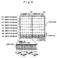
- the reticule 9, which is the pattern under inspection is divided into two in the vertical direction, the first region 102 being taken as the reference die, i.e., the region for forming the reference pattern to be used as reference data for the pattern under inspection, an the second region 103 being taken as the comparison die for formation of the pattern under inspection.
- the overall reticule 9 is divided into a plurality of inspection areas (8 in this embodiment) in the horizontal direction, each inspection area being sub-divided into 4 divided regions that are included in the reference die 102, these being 4 frames (FR1 to FR4), simultaneously with which the overall inspection region is sub-divided into 4 divided regions that are included in the comparison die 103, these being 4 frames (FR5 to FR8), thereby forming each of the prescribed inspection patterns.
- the first divided region (FR1) and the fifth divided region (FR5) have substantially the same shaped patterns formed therein, as do the second divided region (FR2) and the sixth divided region (FR6), the third divided region (FR3) and the seventh divided region (FR7), and the fourth divided region (FR4) and the eight divided region (FR8).
- Patterns are formed in other inspection regions in the same manner.
- the operation of dividing and sub-dividing the above-noted inspection regions into a plurality of frames can, of course, be executed by software.
- this pattern image data is stored into the comparison pattern image information storage means 712 provided in the image comparison section 71.
- the pattern image data of the second frame FR2 including the reference pattern corresponding to this partial pattern under inspection is first acquired and then stored into the reference pattern image information storage means 721 provided in the comparison section 72.
- this pattern image data is stored into the comparison pattern image information storage means 722 provided in the image comparison section 72.
- pattern image data for all the partial patterns under inspection of the first inspection region and pattern image data for the corresponding reference patterns are sent to the image comparison sections, after which the process moves on to the second inspection region, for which the above-noted operations are executed.
- the reference pattern image information storage means includes pattern image information derived from a pattern having substantially the same shape as the pattern under inspection, and which is obtained from a reference pattern formed on the same pattern holding member as is formed the pattern under inspection.
- the reference pattern that provides the reference pattern image information be disposed near the partial pattern under inspection on the pattern holding member.
- the reference pattern be configured so said to detect a pattern in the substantially same range as the partial pattern under inspection in one inspection step in the partial pattern under inspection as a reference pattern image.
- the operation or detecting the reference pattern image be executed at a prescribed amount of timing before the operation or pattern image detection of the corresponding partial pattern under inspection.
- a real-time comparison is made between pattern image data of partial patterns under inspection stored sequentially in the comparison pattern image information storage means 712, 722, 732, and 742 of the image comparison sections and reference pattern image data corresponding to each partial pattern under inspection stored in the reference pattern image information storage means 713, 723, 733, and 743 in of the image processing sections 715, 725, 735, and 745, and a judgment is made as to whether or not defect information is included in the partial pattern under inspection. If the result of this judgment is that defect information is included in the partial pattern under inspection, that information is sent to a defect information accumulation section 83 provided in the review controller 83 and stored therein.
- the review controller 8 in this embodiment of the present invention further preferably includes a database system 85 that minimally stores digital image data, pattern manufacturing process data, and past defect judgment results, these various stored data being appropriately used to output only the most recent pattern defect information detection results, but also information related to the processing of the most recent pattern defect information thereby providing guidelines to an operator with regard to handling of this partial pattern under inspection defect information.
- a database system 85 that minimally stores digital image data, pattern manufacturing process data, and past defect judgment results, these various stored data being appropriately used to output only the most recent pattern defect information detection results, but also information related to the processing of the most recent pattern defect information thereby providing guidelines to an operator with regard to handling of this partial pattern under inspection defect information.
- defect information output from each of the image processing sections be temporarily stored in the defect memories 716, 726, 736, and 746 provided in each one of the image processing sections 715, 725, 735, and 745 formed in each one of the comparison sections 71 to 74, respectively.
- a method for pattern inspection according to the present invention has the following constitution.
- a method for pattern inspection when detecting pattern defects, has a first step of dividing the pattern under inspection into a pre-established number of regions (frames FR1 to FR8) and sequentially acquiring, via an optical means 4 and 5, image information with regard to partial patterns under inspection in each region, a second step of storing the image information with regard to the partial pattern under inspection acquired by step 1 into comparison pattern information storage means 712, 722, 732, and 742 provided in each of a pre-established plurality Of image comparison sections 71 and 74, a third step of, in the image processing means 715, 725, 735, and 745 provided in each individual image comparison section 71 to 74, performing a comparison between the image information with regard to the partial patterns under inspection stored in the comparison pattern image information storage means 712, 722, 732, and 742 and reference pattern image information (reference image information) corresponding to the partial pattern under inspection in the divided regions, which is stored beforehand in reference pattern image information storage means 713, 723, 733, and 7
- the prescribed number of the image comparison sections be set as a number that is smaller than the number of divided regions with regard to the partial pattern under inspection.
- the reference pattern image information in the present invention is preferably a database that is made of digital image data generated at the time of forming the pattern.
- the pattern image information be derived from a pattern having substantially the same shape as the pattern under inspection, and which is obtained from a reference pattern formed on the same pattern holding member as is formed the pattern under inspection.
- the pattern that provides the reference pattern image information be disposed near the partial pattern under inspection on the pattern holding member. Additionally, it is desirable in this embodiment that the reference pattern be configured so said to detect a pattern in the substantially same range as the partial pattern under inspection in one inspection step in the partial pattern under inspection as a reference pattern image.
- the operation of detecting the reference pattern image be executed at a prescribed amount of time before the operation of pattern image detection of the corresponding partial pattern under inspection.
- the reference pattern image information storage means minimally has stored therein either reference pattern image information from a database corresponding to a pattern under inspection selected from a digital image database, or reference pattern image information that is image data obtained via the optical means from the reference pattern held in the pattern holding member.
- image data indicating defects in a prescribed pattern under inspection is all sequentially stored into a defect information accumulation means 83 provided in the review controller 8.
- the first embodiment of the present invention is shown as a reticule inspection apparatus 100.
- This apparatus has an XY stage 3 onto which is set a reticule 9, a laser scanning optical apparatus 4, which scans a laser beam in the Y direction and collects transmitted light, a transmitted light detection section 5 for detecting collected transmitted light, an optical image input distribution section 6, which obtains an image signal from the transmitted light detection section 5, generates an optical image, and distributes this to each image comparison section 71 to 74, an overall controller 2 that performs control of the XY stage 3 and the laser scanning optical apparatus 4, image comparison sections 71 to 74 which compare a reference image synthesized from intermediate data with an optical image so as to detect a pattern defect, and a review controller 8, which collects, accumulates, and edit said defect information (including defect images) from each image comparison section 71 to 74 in real time and, in response to a request, searches and displays defect images.
- a laser scanning optical apparatus 4 which scans a laser beam in the Y direction and collects transmitted light
- a transmitted light detection section 5 for detecting collected transmitted light
- the laser scanning optical apparatus 4 an the transmitted light detection section 5 using a mercury lamp and a CCD line sensor.
- the descriptive data used to describe the reticule 9 to be inspected is acquired by the described data input section 11, and this is converted for each frame into reference image intermediate data by the data converter 12, this being then sent to each image comparison section 71 to 74 via a common memory 15.
- the overall control CPU 21 sends a command to the stage controller 22 and the optical system controller 23, and acquisition of optical images begins.
- the XY stage 3 is caused to move at a fixed speed in the X direction, and for fixed pitch of movement or in the X direction, the laser light is scanned in the Y direction by the laser scanning optical apparatus 4 and the transmitted light is detected by the transmitted light detection section 5, the detected image signals being formed into a two-dimensional image by the image input section 61 provided in the optical image input distribution section 6.
- images for the second through the eight frames are sequentially acquired, so as to obtain the optical images for all eight frames of the first inspection region.
- the XY stage 3 is moved in the opposite direction (-X direction) at a constant speed and the same type of operation is performed. This series of operations is repeated, so as to perform image acquisition and inspection of the entire reticule.
- the two-dimensional optical image formed by the image input section 61 is divided into individual frames by control of the timing generation section 62, and written into individual frame buffers 631 to 634.
- the timing generator 62 has set in it by the overall control CPU 21 the number of scan lines for one frame and the number of overlapping lines between frames, an image acquisition start signal from the overall control CPU 21 causes image acquisition to begin, the number of lines input being monitored and the write frame buffer being selected.
- the first captured frame (FR1) is written into the frame buffer 631 for channel 1 transfer, and simultaneously with completion of transfer into the frame memory 712 of the image comparison section 71 begins.
- the image input section 61 acquires the next frame (FR2) without any waiting time, and performs writing into the frame buffer 632 for channel 2 transfer, after which the frame buffers are sequentially switched so as to write into frame buffers up to the frame buffer 634.
- the time between the writing into one buffer and the time at which that frame is again written (overwritten) corresponds to the time form processing the image of one frame (cycle time), so that it is necessary to complete processing by each image comparison section during the cycle time.
- the reference image that is compared is generated in real time for each frame comparison processing at the reference pattern image information storage means.
- the inspection processing is processing in which the reference pattern image data is converted to intermediate data that is easily expandable from descriptive image data by the data converter 12, this being transferred, via the shared memory 15, to the shared memory of each image comparison section.
- the reference image intermediate data for the first frame (FR1) is extracted from the shared memory 714, the reference image data is expanded to a bit map, an defocusing processing is applied to generate a reference image.
- the defocusing processing is required in order to approximate the image optically obtained from the object of comparison using the reference image.
- the reference image is synchronized to the optical image and transferred from the reference image generation section 713 to the image processing section 715.
- the reference pattern image information storage means 713 When the transfer of the reference image to the image processing section 715 is completed, the reference pattern image information storage means 713 immediately extracts the reference image intermediate data of the next frame (FR5) from the shared memory 714, and generates a reference image. That is, at the image generation section 713, the reference image for the next frame to be compared is always performed beforehand, so that there is no waiting time at the image processing section 715.
- comparison pattern image information which is an optical image transferred to the frame memory 715 is compared with a reference image generated at the reference pattern image information storage means 713 are compared in units of frames to detect defects and, if a defect is detected, the defect information is written into the defect memory 716.
- the defect memory 715 transfers defect information to the defect information accumulation section 83 of the review controller 8 in real time.
- the route of writing reference pattern data and inspection control information that is the route from the shared memory 15 to the shared memory 14 is totally independent from the route of sending the defect information, this being from the defect memory 716 to the defect information accumulation section 83, it is possible to transmit defect information without interrupting the inspection process.
- a review control CPU 81 provided in the review controller 8 collects defect information of each of the image comparison sections 71 to 74 that was accumulated in the defect information accumulation section 83, taking into consideration the number of overlap lines between frames, and generates defect information for the overall reticule.
- a result outputting section 84 can output and review defect information accumulated in the defect information accumulation section 83.
- defect position information is sent to the inspection control CPU via the shared memory 82, and only the part of interest is re-inspected.
- a die-to-die inspection whereby the same pattern disposed at different locations on one and the same reticule is described below.
- Fig. 5 illustrates the operation in a die-to-die inspection according to the present invention
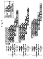
- Fig. 6 is a timing diagram illustrating die-to-die inspection according to the present invention.
- an optical image of a reference die is acquired and accumulated in a DIE memory, after which when an optical image of a die to be compared is captured, a comparison is performed by extracting one frame at a time from the DIE memory so as to detect defects.
- the inspection processing is processing whereby an inspection control CPU 14 calculates beforehand the overall number of frames to be handled as reference dies, that is, as comparison pattern images and the starting frame number for the comparison dies, these being transferred to each image comparison section via a shared memory.
- the overall number of reference die frames is 4, and the starting frame for the comparison die is 5.
- the overall control CPU 21 sends a command to the stage controller 22 and the optical system controller 23, so as to start optical image acquisition.
- control of the timing generator 62 is done to perform sequential divisions into frames, which are written into the frame buffers 631 to 634, and transferred to the image comparison sections.
- the image processing section 715 reads from the shared memory 714 the overall number of frames in the reference die and the starting frame number of the comparison die, and enables the DIE memory 711, which is one of the reference pattern image information storage means, a frame that is transferred from the frame buffer 631 being sequentially written into the DIE memory 711, frames being accumulated until the total number of frames to be written is reached.
- the image processing section 715 enables the frame memory 712, and an optical image from the frame buffer 631 is accepted by the frame memory 712.
- the image processing section 715 extracts the first frame (FR1) from the DIE memory 711 as the reference frame, compares this with an optical image (FR6) of the comparison frame obtained from the frame memory 712, and performs a defect inspection.
- the image processing section 715 writes the defect information into the defect memory 716, and sends the defect information to the detect information accumulation section 83 of the review controller 8 in real time.
- the route of writing the reference image data and inspection control information which is from the shared memory 15 to the shared memory 714, is total independent from the route of outputting the defect information, form the defect memory 716 to the defect information accumulation section 83, it is possible to sent defect information without interrupting the inspection.
- the present invention achieves a number of effects.
- a second effect achieved by the present invention is that, because the review controller is independent from the inspection controller, it is possible to add sophisticated functions such as a database function or an exposure simulation function for operation during inspection, thereby improving the productivity of the apparatus.
Landscapes
- Physics & Mathematics (AREA)
- Health & Medical Sciences (AREA)
- Life Sciences & Earth Sciences (AREA)
- Chemical & Material Sciences (AREA)
- Analytical Chemistry (AREA)
- Biochemistry (AREA)
- General Health & Medical Sciences (AREA)
- General Physics & Mathematics (AREA)
- Immunology (AREA)
- Pathology (AREA)
- Investigating Materials By The Use Of Optical Means Adapted For Particular Applications (AREA)
- Testing Or Measuring Of Semiconductors Or The Like (AREA)
- Preparing Plates And Mask In Photomechanical Process (AREA)
- Image Processing (AREA)
- Image Analysis (AREA)
Applications Claiming Priority (2)
| Application Number | Priority Date | Filing Date | Title |
|---|---|---|---|
| JP17129399A JP2001005166A (ja) | 1999-06-17 | 1999-06-17 | パターン検査方法及びパターン検査装置 |
| JP17129399 | 1999-06-17 |
Publications (2)
| Publication Number | Publication Date |
|---|---|
| EP1061360A2 true EP1061360A2 (fr) | 2000-12-20 |
| EP1061360A3 EP1061360A3 (fr) | 2002-08-21 |
Family
ID=15920627
Family Applications (1)
| Application Number | Title | Priority Date | Filing Date |
|---|---|---|---|
| EP00112910A Withdrawn EP1061360A3 (fr) | 1999-06-17 | 2000-06-19 | Méthode et dispositif pour l'inspection de motifs |
Country Status (3)
| Country | Link |
|---|---|
| US (1) | US6674889B1 (fr) |
| EP (1) | EP1061360A3 (fr) |
| JP (1) | JP2001005166A (fr) |
Cited By (2)
| Publication number | Priority date | Publication date | Assignee | Title |
|---|---|---|---|---|
| WO2004061439A1 (fr) * | 2002-12-19 | 2004-07-22 | Freescale Semiconductor, Inc. | Conversion des coordonnees de defauts de plaquette detectees |
| CN109085466A (zh) * | 2018-07-13 | 2018-12-25 | 上海华力集成电路制造有限公司 | 光罩静电释放缺陷检测方法 |
Families Citing this family (20)
| Publication number | Priority date | Publication date | Assignee | Title |
|---|---|---|---|---|
| JP3762244B2 (ja) * | 2001-03-29 | 2006-04-05 | 株式会社東芝 | 図形データ展開方法 |
| GB2389178B (en) * | 2001-12-31 | 2004-10-27 | Orbotech Ltd | Method for inspecting patterns |
| JP4126189B2 (ja) * | 2002-04-10 | 2008-07-30 | 株式会社日立ハイテクノロジーズ | 検査条件設定プログラム、検査装置および検査システム |
| TWI230343B (en) * | 2002-05-03 | 2005-04-01 | Chi Mei Optoelectronics Corp | A method for classifying a substrate |
| US20040086166A1 (en) * | 2002-11-01 | 2004-05-06 | Photon Dynamics, Inc. | Method and apparatus for flat patterned media inspection |
| US7453798B2 (en) * | 2004-02-19 | 2008-11-18 | Internationl Business Machines Corporation | Active flow management with hysteresis |
| US20060051687A1 (en) * | 2004-09-07 | 2006-03-09 | Takema Ito | Inspection system and inspection method for pattern profile |
| JP4654022B2 (ja) * | 2004-12-24 | 2011-03-16 | 株式会社サキコーポレーション | 基板の外観検査装置 |
| JP4699883B2 (ja) * | 2005-11-30 | 2011-06-15 | 株式会社日立ハイテクノロジーズ | 外観検査装置 |
| JP5042494B2 (ja) * | 2005-12-22 | 2012-10-03 | インテル コーポレイション | 散乱光の角度分布を使ったマスクブランクの欠陥の検出および特性評価 |
| WO2009031303A1 (fr) * | 2007-09-05 | 2009-03-12 | Tohoku University | Élément d'imagerie à semi-conducteurs et dispositif d'imagerie |
| US8379229B2 (en) * | 2008-02-14 | 2013-02-19 | Seiko Epson Corporation | Simulation of a printed dot-pattern bitmap |
| JP4554691B2 (ja) * | 2008-02-25 | 2010-09-29 | アドバンスド・マスク・インスペクション・テクノロジー株式会社 | 補正パターン画像生成装置、パターン検査装置および補正パターン画像生成方法 |
| US8564799B2 (en) * | 2010-03-10 | 2013-10-22 | Xerox Corporation | Print quality validation of print jobs using bitmapped image |
| US8661293B2 (en) | 2011-06-30 | 2014-02-25 | International Business Machines Corporation | Test architecture based on intelligent test sequence |
| US9196031B2 (en) * | 2012-01-17 | 2015-11-24 | SCREEN Holdings Co., Ltd. | Appearance inspection apparatus and method |
| US9858658B2 (en) * | 2012-04-19 | 2018-01-02 | Applied Materials Israel Ltd | Defect classification using CAD-based context attributes |
| US9595091B2 (en) | 2012-04-19 | 2017-03-14 | Applied Materials Israel, Ltd. | Defect classification using topographical attributes |
| KR102135177B1 (ko) * | 2014-06-27 | 2020-07-20 | 한국전자통신연구원 | 능동형 이미징 시스템 구현 방법 및 장치 |
| JP7222671B2 (ja) * | 2018-11-19 | 2023-02-15 | 株式会社ニューフレアテクノロジー | パターン検査装置及びパターン検査方法 |
Citations (2)
| Publication number | Priority date | Publication date | Assignee | Title |
|---|---|---|---|---|
| JPH06325162A (ja) * | 1993-05-11 | 1994-11-25 | Nikon Corp | 画像処理装置 |
| EP0952488A2 (fr) * | 1998-04-24 | 1999-10-27 | Nec Corporation | Appareil pour contrÔler des masques avec temps d'inspection réduit |
Family Cites Families (14)
| Publication number | Priority date | Publication date | Assignee | Title |
|---|---|---|---|---|
| JPS59128419A (ja) * | 1983-01-13 | 1984-07-24 | Toppan Printing Co Ltd | 印刷物検査装置 |
| JPS59157505A (ja) * | 1983-02-28 | 1984-09-06 | Hitachi Ltd | パタ−ン検査装置 |
| JPH01305477A (ja) | 1988-06-02 | 1989-12-08 | Hitachi Ltd | 外観欠陥検査方法 |
| JPH02108947A (ja) * | 1988-10-19 | 1990-04-20 | Matsushita Electron Corp | ホトマスク検査装置 |
| IL125216A (en) | 1990-12-04 | 2001-07-24 | Orbot Instr Ltd | Apparatus and method for microscopic inspection of articles |
| JP3187859B2 (ja) * | 1991-05-22 | 2001-07-16 | 株式会社日立製作所 | マスクのパターンデータ作成方法および製造方法 |
| JPH04365045A (ja) | 1991-06-12 | 1992-12-17 | Fujitsu Ltd | レチクルパターン検査装置 |
| US5577171A (en) * | 1992-03-02 | 1996-11-19 | Kabushiki Kaisha Toshiba | Figure pattern generating apparatus for detecting pattern defects |
| US5777901A (en) * | 1995-09-29 | 1998-07-07 | Advanced Micro Devices, Inc. | Method and system for automated die yield prediction in semiconductor manufacturing |
| US6064484A (en) * | 1996-03-13 | 2000-05-16 | Fujitsu Limited | Pattern inspection method and system |
| JP2776416B2 (ja) | 1996-05-07 | 1998-07-16 | 日本電気株式会社 | レチクル外観検査装置 |
| JPH10141932A (ja) * | 1996-11-07 | 1998-05-29 | Fujitsu Ltd | パターン検査方法と装置 |
| US6381356B1 (en) * | 1996-10-23 | 2002-04-30 | Nec Corporation | Method and apparatus for inspecting high-precision patterns |
| JP2984635B2 (ja) | 1996-10-23 | 1999-11-29 | 日本電気株式会社 | 高精度パターンの外観の検査方法および装置 |
-
1999
- 1999-06-17 JP JP17129399A patent/JP2001005166A/ja active Pending
-
2000
- 2000-06-19 US US09/597,701 patent/US6674889B1/en not_active Expired - Fee Related
- 2000-06-19 EP EP00112910A patent/EP1061360A3/fr not_active Withdrawn
Patent Citations (2)
| Publication number | Priority date | Publication date | Assignee | Title |
|---|---|---|---|---|
| JPH06325162A (ja) * | 1993-05-11 | 1994-11-25 | Nikon Corp | 画像処理装置 |
| EP0952488A2 (fr) * | 1998-04-24 | 1999-10-27 | Nec Corporation | Appareil pour contrÔler des masques avec temps d'inspection réduit |
Cited By (5)
| Publication number | Priority date | Publication date | Assignee | Title |
|---|---|---|---|---|
| WO2004061439A1 (fr) * | 2002-12-19 | 2004-07-22 | Freescale Semiconductor, Inc. | Conversion des coordonnees de defauts de plaquette detectees |
| US6882745B2 (en) | 2002-12-19 | 2005-04-19 | Freescale Semiconductor, Inc. | Method and apparatus for translating detected wafer defect coordinates to reticle coordinates using CAD data |
| CN100582754C (zh) * | 2002-12-19 | 2010-01-20 | 飞思卡尔半导体公司 | 检测晶圆缺陷的系统和方法 |
| CN109085466A (zh) * | 2018-07-13 | 2018-12-25 | 上海华力集成电路制造有限公司 | 光罩静电释放缺陷检测方法 |
| CN109085466B (zh) * | 2018-07-13 | 2020-11-20 | 上海华力集成电路制造有限公司 | 光罩静电释放缺陷检测方法 |
Also Published As
| Publication number | Publication date |
|---|---|
| JP2001005166A (ja) | 2001-01-12 |
| US6674889B1 (en) | 2004-01-06 |
| EP1061360A3 (fr) | 2002-08-21 |
Similar Documents
| Publication | Publication Date | Title |
|---|---|---|
| US6674889B1 (en) | Pattern inspection method and pattern inspection apparatus | |
| US6882745B2 (en) | Method and apparatus for translating detected wafer defect coordinates to reticle coordinates using CAD data | |
| JP3201471B2 (ja) | レティクル検査装置 | |
| US10026011B2 (en) | Mask inspection apparatus, mask evaluation method and mask evaluation system | |
| JP6769971B2 (ja) | 焦点体積方法を用いたウェーハ検査 | |
| CN109659245B (zh) | 监测光掩模缺陷率的改变 | |
| US7869643B2 (en) | Advanced cell-to-cell inspection | |
| JP2009071136A (ja) | データ管理装置、検査システムおよび欠陥レビュー装置 | |
| JP4336672B2 (ja) | 試料検査装置、試料検査方法及びプログラム | |
| KR960013357B1 (ko) | 화상데이타 검사방법 및 장치 | |
| JP4564768B2 (ja) | パターン検査方法及びその装置 | |
| JP2011222636A (ja) | 検査装置,検査方法、及び欠陥座標補正方法 | |
| JP2000088563A (ja) | 外観検査方法および外観検査装置 | |
| JP2004212221A (ja) | パターン検査方法及びパターン検査装置 | |
| US7275006B2 (en) | Workpiece inspection apparatus assisting device, workpiece inspection method and computer-readable recording media storing program therefor | |
| US6973208B2 (en) | Method and apparatus for inspection by pattern comparison | |
| JP3752849B2 (ja) | パターン欠陥検査装置及びパターン欠陥検査方法 | |
| US6477265B1 (en) | System to position defect location on production wafers | |
| US20070172111A1 (en) | Inspection apparatus of object to be inspected | |
| JP3762244B2 (ja) | 図形データ展開方法 | |
| US6188785B1 (en) | Pattern inspecting apparatus and inspecting method | |
| JP2000180377A (ja) | 欠陥・異物検査装置 | |
| JP4977123B2 (ja) | 試料検査装置、試料検査方法及びプログラム | |
| JP2006113073A (ja) | パターン欠陥検査装置及びパターン欠陥検査方法 | |
| JP2009188175A (ja) | 外観検査装置及び外観検査方法 |
Legal Events
| Date | Code | Title | Description |
|---|---|---|---|
| PUAI | Public reference made under article 153(3) epc to a published international application that has entered the european phase |
Free format text: ORIGINAL CODE: 0009012 |
|
| AK | Designated contracting states |
Kind code of ref document: A2 Designated state(s): AT BE CH CY DE DK ES FI FR GB GR IE IT LI LU MC NL PT SE |
|
| AX | Request for extension of the european patent |
Free format text: AL;LT;LV;MK;RO;SI |
|
| PUAL | Search report despatched |
Free format text: ORIGINAL CODE: 0009013 |
|
| AK | Designated contracting states |
Kind code of ref document: A3 Designated state(s): AT BE CH CY DE DK ES FI FR GB GR IE IT LI LU MC NL PT SE |
|
| AX | Request for extension of the european patent |
Free format text: AL;LT;LV;MK;RO;SI |
|
| 17P | Request for examination filed |
Effective date: 20021111 |
|
| AKX | Designation fees paid |
Designated state(s): DE FR GB |
|
| 17Q | First examination report despatched |
Effective date: 20040217 |
|
| STAA | Information on the status of an ep patent application or granted ep patent |
Free format text: STATUS: THE APPLICATION IS DEEMED TO BE WITHDRAWN |
|
| 18D | Application deemed to be withdrawn |
Effective date: 20050804 |