EP1061608A2 - Connecteurs électriques entre deux plaquettes à circuits imprimés - Google Patents
Connecteurs électriques entre deux plaquettes à circuits imprimés Download PDFInfo
- Publication number
- EP1061608A2 EP1061608A2 EP00109893A EP00109893A EP1061608A2 EP 1061608 A2 EP1061608 A2 EP 1061608A2 EP 00109893 A EP00109893 A EP 00109893A EP 00109893 A EP00109893 A EP 00109893A EP 1061608 A2 EP1061608 A2 EP 1061608A2
- Authority
- EP
- European Patent Office
- Prior art keywords
- contact
- conductive member
- section
- circuit
- electrical connector
- Prior art date
- Legal status (The legal status is an assumption and is not a legal conclusion. Google has not performed a legal analysis and makes no representation as to the accuracy of the status listed.)
- Withdrawn
Links
Images


Classifications
-
- H—ELECTRICITY
- H01—ELECTRIC ELEMENTS
- H01R—ELECTRICALLY-CONDUCTIVE CONNECTIONS; STRUCTURAL ASSOCIATIONS OF A PLURALITY OF MUTUALLY-INSULATED ELECTRICAL CONNECTING ELEMENTS; COUPLING DEVICES; CURRENT COLLECTORS
- H01R13/00—Details of coupling devices of the kinds covered by groups H01R12/70 or H01R24/00 - H01R33/00
- H01R13/02—Contact members
- H01R13/22—Contacts for co-operating by abutting
- H01R13/24—Contacts for co-operating by abutting resilient; resiliently-mounted
- H01R13/2407—Contacts for co-operating by abutting resilient; resiliently-mounted characterized by the resilient means
- H01R13/2414—Contacts for co-operating by abutting resilient; resiliently-mounted characterized by the resilient means conductive elastomers
-
- H—ELECTRICITY
- H01—ELECTRIC ELEMENTS
- H01R—ELECTRICALLY-CONDUCTIVE CONNECTIONS; STRUCTURAL ASSOCIATIONS OF A PLURALITY OF MUTUALLY-INSULATED ELECTRICAL CONNECTING ELEMENTS; COUPLING DEVICES; CURRENT COLLECTORS
- H01R12/00—Structural associations of a plurality of mutually-insulated electrical connecting elements, specially adapted for printed circuits, e.g. printed circuit boards [PCB], flat or ribbon cables, or like generally planar structures, e.g. terminal strips, terminal blocks; Coupling devices specially adapted for printed circuits, flat or ribbon cables, or like generally planar structures; Terminals specially adapted for contact with, or insertion into, printed circuits, flat or ribbon cables, or like generally planar structures
- H01R12/70—Coupling devices
- H01R12/71—Coupling devices for rigid printing circuits or like structures
- H01R12/712—Coupling devices for rigid printing circuits or like structures co-operating with the surface of the printed circuit or with a coupling device exclusively provided on the surface of the printed circuit
- H01R12/714—Coupling devices for rigid printing circuits or like structures co-operating with the surface of the printed circuit or with a coupling device exclusively provided on the surface of the printed circuit with contacts abutting directly the printed circuit; Button contacts therefore provided on the printed circuit
-
- H—ELECTRICITY
- H03—ELECTRONIC CIRCUITRY
- H03K—PULSE TECHNIQUE
- H03K2217/00—Indexing scheme related to electronic switching or gating, i.e. not by contact-making or -breaking covered by H03K17/00
- H03K2217/94—Indexing scheme related to electronic switching or gating, i.e. not by contact-making or -breaking covered by H03K17/00 characterised by the way in which the control signal is generated
- H03K2217/96—Touch switches
- H03K2217/9607—Capacitive touch switches
- H03K2217/960755—Constructional details of capacitive touch and proximity switches
- H03K2217/96076—Constructional details of capacitive touch and proximity switches with spring electrode
-
- H—ELECTRICITY
- H05—ELECTRIC TECHNIQUES NOT OTHERWISE PROVIDED FOR
- H05K—PRINTED CIRCUITS; CASINGS OR CONSTRUCTIONAL DETAILS OF ELECTRIC APPARATUS; MANUFACTURE OF ASSEMBLAGES OF ELECTRICAL COMPONENTS
- H05K1/00—Printed circuits
- H05K1/02—Details
- H05K1/11—Printed elements for providing electric connections to or between printed circuits
-
- H—ELECTRICITY
- H05—ELECTRIC TECHNIQUES NOT OTHERWISE PROVIDED FOR
- H05K—PRINTED CIRCUITS; CASINGS OR CONSTRUCTIONAL DETAILS OF ELECTRIC APPARATUS; MANUFACTURE OF ASSEMBLAGES OF ELECTRICAL COMPONENTS
- H05K3/00—Apparatus or processes for manufacturing printed circuits
- H05K3/30—Assembling printed circuits with electric components, e.g. with resistors
- H05K3/32—Assembling printed circuits with electric components, e.g. with resistors electrically connecting electric components or wires to printed circuits
- H05K3/325—Assembling printed circuits with electric components, e.g. with resistors electrically connecting electric components or wires to printed circuits by abutting or pinching; Mechanical auxiliary parts therefor
-
- H—ELECTRICITY
- H05—ELECTRIC TECHNIQUES NOT OTHERWISE PROVIDED FOR
- H05K—PRINTED CIRCUITS; CASINGS OR CONSTRUCTIONAL DETAILS OF ELECTRIC APPARATUS; MANUFACTURE OF ASSEMBLAGES OF ELECTRICAL COMPONENTS
- H05K3/00—Apparatus or processes for manufacturing printed circuits
- H05K3/36—Assembling printed circuits with other printed circuits
- H05K3/368—Assembling printed circuits with other printed circuits parallel to each other
Definitions
- the present invention relates to intermediate electrical connectors.
- An intermediate electrical connector is used to connect two circuit broads or corresponding circuit portions of connection objects.
- the intermediate electrical connector comprises a support plate of dielectric material and a conductive member extending through the support member.
- the conductive member is a molding of a conductive elastomer or a mixture of elastic polymeric material and conductive powder.
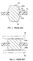
- Fig. 1 shows an example which comprises a support member 51 of dielectric material and a conductive member 52 with upper and lower conic surfaces 52A attached thereto by integral molding.
- the upper and lower flat end faces 53 and 54 make elastic contact with the circuit portions of connection objects.
- the number of conductive members 52 provided on the support member 51 corresponds to the number of circuit portions of the connection objects.
- connection objects or circuit boards 55 and 56 are provided on both sides of the support member 51.
- the circuit boards 55 and 56 have circuit portions 55A and 56B which are pressed against the contact faces 53 and 54, compressing the conductive member 52.
- the two circuit portions 55A and 56B of the circuit boards 55 and 56 are connected to the conductive member 52 and short-circuited via the conductive member 52.
- the above conventional intermediate electrical connector provides no satisfactory amount of elastic deformation of the conductive member 52. Since the conductive member 52 increases in diameter from the upper and lower contact faces 53 and 54 to the support member 51 and held by the edges of the support aperture 51A, not only the pressure upon the contact face 53 is distributed to the whole body but also a tension is produced on the conic surface 52 between the flange portion 52B and the contact face 53 of the conductive member 52, providing no satisfactory amount of deformation.
- the conductive elastomer has such a tendency that when compressed, its resistivity in the compression direction decreases. However, the amount of elastic deformation is so small that the contact resistance is high.
- the conductive elastomer When it is compressed, the conductive elastomer decreases in electrical resistance at the initial, stage but increases in electrical resistance beyond the initial stage. Thus, when it is compressed beyond the initial compression stage, the electrical characteristics deteriorates even though the mechanical contact is improved. In addition, if this high compression is applied to a number of conductive members, the combined force applied to the mating circuit boards is disadvantageously high.
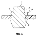
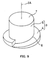
- a support plate 1 is made of dielectric material.
- a plurality of support apertures 2 having an inside diameter D1 are provided in the support plate 1, and a plurality of conductive members 3 are attached thereto by integral molding such that each conductive member 3 is held by the circumferential edges of each support aperture 2.
- Preferred examples of the dielectric material include films of polyimide, polyester, and polyamide
- the conductive member 3 is made by mixing an elastic polymeric material with a conductive powder or particles.
- the elastic polymers are silicone rubber, polybutadiene rubber, natural rubber, polyisoprene, styrene-butadiene copolymer rubber, acrylonitrile-butadiene copolymer rubber, ethylene-propylene copolymer rubber, urethane rubber, polyester rubbers, chloroprene rubber, epichlorohydrin rubber, and soft liquid epoxy rubber.
- the conductive powder or particles mixed with the elastic polymeric material include one or more of powder, granules, chips, flakes, and amorphous materials of gold, silver, nickel, copper, tin, aluminum, palladium, and carbon. Especially, flakes of silver are preferred. It is preferred that silver powder is treated with an organic silicon compound.
- the conductive member 3 has a retention section 4 and an elastic protruded section 5.
- the retention section 4 is brought into contact with the inside wall of the support aperture 2 and the upper and lower surfaces of the support plate 1 so as to cover the edges of the support aperture 2 of the inside diameter D1.
- the protruded section 5 has shoulder portions 6 next to the retention section 4 and takes a cylindrical form having an outside diameter D2 and flat contact faces 7 at opposite ends.
- the outside diameter D2 is smaller than the inside diameter D1 of the support aperture 2 so that the protruded section 5 is situated within radial range of their support aperture 2.
- the shoulder portions 6 are rounded as shown by R in the figure.
- the intermediate electrical connector operates as follows.
- connection objects or circuit boards 11 and 2 are provided on both sides of the support plate 1 and fixed at predetermined positions by proper means.
- the circuit boards 11 and 12 have circuit portions 11A and 12A, respectively, which are pressed against the contact faces 7 of the conductive member 3 when the circuit boards 11 and 12 are situated at the predetermined positions.
- the elastic protruded section 5 Since the elastic protruded section 5 is situated within the radial range of the support aperture 2, it is able to undergo large elastic deformation in the vertical direction regardless of the presence of the retention section 4.
- the amount of elastic deformation of the protruded section 5 is sufficiently large to absorb variations of the conductive members 3 and the circuit boards 11 and 12, thus ensuring good contacts of the conductive members 3 under satisfactory contact pressure.
- the large amount of compression of the conductive members 3 reduces the electrical resistance.
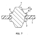
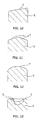
- the shoulder portions 6 are formed with tilted surfaces.
- one shoulder portion 6 is provided on one of the sides and a conic section is provided on the other side to produce the same effects on the side where the shoulder portion is provided.
- the protruded section 5 takes a pair of upward and downward conic shapes with shoulder portions 6 next to the retention section 4.
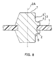
- Fig. 8 the shape on the right side of an axis 2A is identical with the shape of Fig. 1 and the left side with the shape of Fig. 1 to produce a large amount of elastic deformation on the right side so that the conductive member 7 slide laterally relative to the circuit boards, producing the wiping effects.
- the thickness of the retention section 4 changes in spiral manner to allow a large amount of elastic deformation of the protruded section 5 and produce twisting movement around the axis 2A, thereby producing the wiping effects relative to the circuit boards.
- the contact face 7 has a conical surface to reduce the contact area with a mating object, which is prone to corrosion, so as to increase the Hertz stress and ensure the contact stability.
- a concave surface 7 is provided on the contact area to produce the suction effects, thereby assuring firm contact.
- the depth of the concave surface 7 is determined to match the solder ball or the like of a mating object as shown by phantom line. If the contact surface is provided with many fine projections, the wiping effects are produced at random.
- the conductive member is made of conductive elastomer so as to have a retention section for engagement with the edges of a support aperture of a support plate and an elastic protruded section extending from the retention section in the direction of thickness of the support plate.
- the retention section has flange portions extending in the radial direction of the support aperture.
- the elastic protruded section has a pair of contact portions for elastic contact with the circuit portions of connection objects. There are provided shoulder portions between the protruded section and the retention section.
- the diameter of the shoulder portions is smaller than the diameter of the support aperture so that upon contact with connection objects, the elastic protruded section is able to undergo large elastic deformation regardless of the presence of the retention section, thereby providing a sufficient amount of deformation to absorb variations of the conductive members and connection objects to thereby ensure stable connections.
- the large amount of compression reduces the contact resistance of the conductive members, thereby providing good electrical connections.
- a support plate 1 is made of dielectric material.
- a plurality of support apertures 2 having an inside diameter D1 are provided in the support plate 1, and a plurality of conductive members 3 are attached thereto by integral molding such that each conductive member 3 is held by the circumferential edges 2A of each support aperture 2.
- Preferred examples of the dielectric material include films of polyimide, polyester, and polyamide
- the conductive member 3 is made by mixing elastic polymeric material with conductive powder or particles.
- the elastic polymers are silicone rubber, polybutadiene rubber, natural rubber, polyisoprene, styrene-butadiene copolymer rubber, acrylonitrile-butadiene copolymer rubber, ethylene-propylene copolymer rubber, urethane rubber, polyester rubbers, chloroprene rubber, epichlorohydrin rubber, and soft liquid epoxy rubber.
- Examples of the conductive powder or particles ixed with the elastic polymeric material include one or more of powder, granules, chips, flakes, and amorphous materials of gold, silver, nickel, copper, tin, aluminum, palladium, and carbon. Especially, flakes of silver are preferred. It is preferred that silver powder is treated with an organic silicon compound.
- the conductive member 3 has a retention section 4 and an elastic protruded section 5.
- the retention section 4 is brought into contact with the inside wall of the support aperture 2 and the upper and lower surfaces of the support plate 1 so as to cover the edges 2A of the support aperture 2.
- the conductive member 3 is integrally molded with the support member 1.
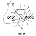
- the protruded section 5 has upward and downward extending sections 5A and 5B.
- the upward extending section 5A has a conic side and a displacement means or recess 6 at the top surface, forming an annular bearing face 7A.
- the downward extending section 5B has a conic side having an outside diameter smaller than the outside diameter of the upward extending section 5A but substantially equal to the inside diameter of the displacement recess 6 and is situated at a position corresponding to the displacement recess 6. Also, it has a circular bearing face 7B having a diameter substantially equal to the inside diameter of the displacement recess 6.
- the intermediate electrical connector operates as follows.
- connection objects or circuit boards are provided on both sides of the support plate 1 and fixed at predetermined positions by proper means.
- the circuit boards have circuit portions, respectively, which are pressed against the bearing faces 7A and 7B of the conductive member 3 when the circuit boards are situated at the predetermined positions.
- the upward extending section 5A is compressed in the direction of an arrow A by the pressure on the bearing face 7A while the downward extending section 5B is compressed in the direction of an arrow B by the pressure on the bearing face 7B and is displaced into the displacement recess 6 indicated by an arrow F. Consequently, the downward extending section 5B is moved by the sum of the compressed length and displaced distance. Thus, even if the compressed length is small, the total amount of movement is large.
- the contact pressure is smaller than the contact pressure under which the conventional conductive member is moved by the same amount.
- the amount of movement of the elastic protruded section 5 is so large that even if there are variations between the bearing faces 7A and 7B of a number of conductive members 3 and the circuit portions of connection objects, such variations are absorbed satisfactorily. Consequently, under light contact pressures, good contacts are ensured for all of the conductive members 3.
- the compression of the conductive members 3 is so small that the electrical resistance is low, improving the electrical characteristics.
- the upward and downward extending sections 5A and 5B have the same cylindrical side, but their central axes 8A and 8B are offset to form displacement means or spaces 6A and 6B on opposite sides to the bearing faces 7A and 7B, respectively.
- the conductive member 3 is tilted because of its asymmetric shape, increasing the amount of movement.
- the conductive member 3 is held by the central portion in contrast to the above modification wherein the conductive member 3 is held by engagement between the retention flanges 4 and the edges of a support aperture.
- the inside diameter of the support aperture 2 is larger than the outside diameter of the conductive member 3.
- a bridge portion 1A diametrically extends across the support aperture 2.
- the conductive member 3 is spaced from the side face of the support aperture 2 and held by the bridge portion 1A. Since the circumferential face of the conductive member 3 is not fixed, it is easy for the conductive member 3 to tilt, thus increasing the amount of movement.
- a pair of displacement means or cavities 6A and 6B are provided within the conductive member 3. Any number and/or size of the displacement cavities may be provided as far as it is effective for the elastic protruded sections to move. That is, the elastic protruded sections may be made of foam rubber to produce the effects.
- the conductive member is made of conductive elastomer so as to have a retention section for engagement with a support plate and an elastic protruded section extending from the retention section in the direction of thickness of the support plate.
- a displacement means is provided in the conductive member to allow the elastic protruded section to displace so that the bearing face of the protruded section can move to a large extent, thereby providing a sufficient amount of movement to absorb variations in relative positions between the conductive members and connection objects or momentary movement of connection objects, ensuring a stable contact. Since the amount of compression is limited to the proper level, the conductive member maintains the low contact resistance, ensuring the good electrical characteristics.
- a support plate 1 is made of dielectric material.
- a plurality of support apertures 2 are provided in the support plate 1, and a plurality of conductive members 3 are attached thereto by integral molding.
- Preferred examples of the dielectric material are films of polyimide, polyester, and polyamide.
- the conductive member 3 is made of mixing elastic polymeric material with conductive powder or particles.
- the elastic polymers are silicone rubber, polybutadiene rubber, natural rubber, polyisoprene, styrene-butadiene copolymer rubber, acrylonitrile-butadiene copolymer rubber, ethylene-propylene copolymer rubber, urethane rubber, polyester rubbers, chloroprene rubber, epichlorohydrin rubber, and soft liquid epoxy rubber.
- Examples of the conductive powder or particles mixed with the elastic polymeric material include one or more of powder, granules, chips, flakes, and amorphous materials of gold, silver, nickel, copper, tin, aluminum, palladium, and carbon. Especially, flakes of silver are preferred. It is preferred that silver powder is treated with an organic silicon compound.
- the conductive member 3 has retention sections 4 and elastic protruded sections 5.
- the retention sections 4 are brought into contact with the inside wall of the support aperture 2 and the upper and lower surfaces of the support plate 1 so as to cover the edges of the support aperture 2.
- Such a retention structure is obtained by integrally molding the conductive members 3 with the support plate 1.
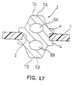
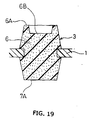
- the protruded sections 5 consists of upper and lower conic sections 6 and 7.
- the lower conic section 7 has a pedestal section with a lower flat contact face 7A while, according to the invention, the upper conic section 6 has a double pedestal sections with first and second contact faces 6A and 6B.
- the first and second contact faces 6A have a flat surface, respectively, to match the flat circuit portions P1A and P2A of circuit boards P1 and P2, respectively, but may have a curbed or tilted surface.
- one of the upper and lower conic sections has a plurality of contact surfaces which are made in the form of a step.
- the distance between the first and second contact faces 6A and 6B is determined by the amount of compression caused by the circuit boards or connection objects.
- the first contact face 6A receives the pressure for compression up to the distance , where the second contact face 6B starts contact for compression.
- The is determined at such a point that the electrical resistance of the conductive member 3 starts to rise under the conditions that only the first contact face 6A receives the compression.
- the intermediate connector operates as follows.
- connection objects or circuit boards P1 and P2 are provided and fixed by proper means on upper and lower sides of the support plate 1 so as to compress the conductor member 3.
- the circuit boards P1 and P2 have a circuit portion P1A or P2A, respectively, so that when they are fixed at the predetermined positions, the circuit portions P1A and P2A press the contact faces 6A, 6B, and 7A of the conductive member 3, respectively.
- the first contact face 6A receives the pressure from the circuit board P1 so that the upper protruded section 6 is compressed in the direction of an arrow A.
- the electrical resistance decreases in the initial stage but starts to increase when the amount of compression reechoes the value .
- the second contact face 6B is brought into contact with the connection object P1 so that the contact area increases so much that the electrical resistance decreases.
- the position of the connection object P1 is determined at a position where the amount of compression is set before the electrical resistance increases after the initial decrease.
- the contact face 7A of the lower protruded section 7 is brought into contact with the lower connection object P2 under a predetermined contact pressure.
- the circuit portions P1A and P2A of the connection objects P1 and P2 are connected to each other with a low electrical resistance and a large amount of movement because of the first and second contact faces 6A and 6B of the upper protruded section. Consequently, variations in the contact positions due to variations in the circuit component positions, warp of the support plate, and dimensions of the conductive member are absorbed satisfactorily while the good electrical characteristics are maintained.
- the lower protruded section 7 may be made so as to have the same structure as the upper protruded section 6.
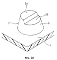
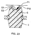
- a recess is provided at the center of a top face so as to form first and second contact faces 6A and 6B.
- the area ratio and the distance between the contact faces 6A and 6B are determined such that the second contact face starts to contact the connection object when the electrical resistance at the first contact face 6A starts to increase with increase of the compression.
- the top face of the upper protruded section 6 is divided into first and second contact faces 6A and 6B by a diametric line.
- the first contact face 6A extends in radial directions, with the remaining area made as the second contact face 6B.
- the second contact face 6B has a concave surface to match the hemispheric circuit portion P1A while the first contact face 6A is flat.
- connection object P1 first makes contact with the first contact face 6A and the second contact face 6B as shown in Fig. 24.
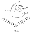
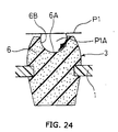
- the upper protruded section 6 has the same structure as that of Fig. 19 while the lower protruded section 7 has the same structure as that of Fig. 18.
- the amount of compression of the first contact face 7A is absorbed by the concave second contact face 6B because the first contact face 7A is situated at a position corresponding to the concave second contact face 6B so that the conductor member 3 as a whole is not compressed very much. That is, a small force to compress is able to provide the above displacement of the first contact face 7A.
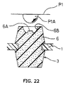
- the first contact face 6A is flat and parallel to the support plate 1 while the second contact face 6B is sloped. Both of the contact faces 6A and 6B make successive contacts with the circuit portion to produce the effects described above according to the invention.
- the sloped face may be curved.
- the above two stepped contact faces with the circuit portion of a connection object may be three or more stepped contacts.
- the various contact faces may be provided on both or either of the upper and lower protruded sections.
- the conductive member 3 has upper and lower flat contact faces 6A and 6B while the upper and lower circuit portions P1A and P2A of connection objects P1 and P2 have raised and indented areas, respectively, so that the conductive member 3 is compressed in stepped manner to produce the same effects as described above. It is sufficient that the circuit portion of either upper or lower contact object is provided with either raised or indented configuration.
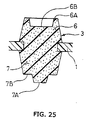
- the conductive member 3 which has a configuration similar to the upper half of the conductive member 3 of Fig. 18, is provided on a circuit portion 1A of the support member 1. It makes successive contacts with the circuit portion P1A of a connection object P1 in the same manner as the conductive member of Fig. 18.
- Such a conductive member as this may be applied to any of the connection methods described in Figs. 18 through 28.
- a plurality of contact faces are provided so that the contact area increases in stepped manner as the conductive member is compressed. Consequently, not only the increase in electrical resistance with the increase in compression is prevented but also large amounts of displacement of the contact faces are assured so that variations in distance between the conductive members and the connection objects are absorbed and the contacts are so stable that the electrical characteristics are improved.
Landscapes
- Coupling Device And Connection With Printed Circuit (AREA)
Applications Claiming Priority (6)
| Application Number | Priority Date | Filing Date | Title |
|---|---|---|---|
| JP12791299A JP3350479B2 (ja) | 1999-05-10 | 1999-05-10 | 中間電気コネクタ |
| JP12791299 | 1999-05-10 | ||
| JP26963299A JP2001094275A (ja) | 1999-11-24 | 1999-09-24 | 中間電気コネクタ |
| JP26963299 | 1999-11-24 | ||
| JP2000007307A JP2001203016A (ja) | 2000-01-17 | 2000-01-17 | 中間電気コネクタ |
| JP2000007307 | 2000-01-17 |
Publications (2)
| Publication Number | Publication Date |
|---|---|
| EP1061608A2 true EP1061608A2 (fr) | 2000-12-20 |
| EP1061608A3 EP1061608A3 (fr) | 2002-10-02 |
Family
ID=27315645
Family Applications (1)
| Application Number | Title | Priority Date | Filing Date |
|---|---|---|---|
| EP00109893A Withdrawn EP1061608A3 (fr) | 1999-05-10 | 2000-05-10 | Connecteurs électriques entre deux plaquettes à circuits imprimés |
Country Status (2)
| Country | Link |
|---|---|
| US (1) | US6280207B1 (fr) |
| EP (1) | EP1061608A3 (fr) |
Cited By (7)
| Publication number | Priority date | Publication date | Assignee | Title |
|---|---|---|---|---|
| WO2003045123A1 (fr) * | 2001-11-16 | 2003-05-30 | R-Tec Corporation | Tapis de contacts intermediaires |
| WO2004038433A1 (fr) | 2002-10-28 | 2004-05-06 | Jsr Corporation | Connecteur en forme de feuille et procede de production et application associee |
| WO2004040762A1 (fr) * | 2002-10-29 | 2004-05-13 | BSH Bosch und Siemens Hausgeräte GmbH | Detecteur capacitif d'approche et/ou de contact et corps en plastique electriquement conducteur pour un detecteur de ce type |
| EP1416636A3 (fr) * | 2002-10-31 | 2005-08-31 | E.G.O. Elektro-Gerätebau GmbH | Elément capteur pour un commutateur capacitif à effleurement avec un élément électriquement conducteur et sa méthode de fabrication |
| EP1577974A3 (fr) * | 2004-03-19 | 2006-01-18 | Hirschmann Electronics GmbH & Co. KG | Dispositif pour contacter une structure d 'antenne, produite par moulage par injection à plusieurs composants |
| DE102007054524A1 (de) | 2007-11-07 | 2009-02-26 | E.G.O. Control Systems Gmbh | Anordnung eines elastischen Körpers in einer Haltevorrichtung |
| EP3679381A1 (fr) * | 2017-09-07 | 2020-07-15 | Technoprobe S.p.A | Élément d'interface pour appareil d'essai de dispositifs électroniques et procédé de fabrication correspondant |
Families Citing this family (17)
| Publication number | Priority date | Publication date | Assignee | Title |
|---|---|---|---|---|
| AU2002222447A1 (en) * | 2000-12-05 | 2002-06-18 | Aprion Digital Ltd. | Board integrated resilient contact elements array and method of fabrication |
| CN1870871B (zh) * | 2002-05-28 | 2011-10-05 | 莫莱克斯公司 | 接插件封装和传送组件 |
| US6799977B2 (en) * | 2002-07-11 | 2004-10-05 | Hewlett-Packard Development Company, L.P. | Socket having foam metal contacts |
| TW547771U (en) * | 2002-07-23 | 2003-08-11 | Via Tech Inc | Elastic electrical contact package structure |
| US6786736B2 (en) * | 2002-08-23 | 2004-09-07 | Artesyn Technologies, Inc. | Surface mount interconnect and device including same |
| DE20321550U1 (de) * | 2003-08-11 | 2007-12-20 | Hirschmann Electronics Gmbh & Co. Kg | Elastische Kontaktelemente zum Einclipsen |
| US6994570B2 (en) * | 2004-01-28 | 2006-02-07 | International Business Machines Corporation | High performance interposer for a chip package using deformable button contacts |
| US7442049B2 (en) * | 2005-02-09 | 2008-10-28 | International Business Machines Corporation | Electrical connecting device and method of forming same |
| US7059867B1 (en) * | 2005-03-30 | 2006-06-13 | Artesyn Technologies, Inc. | High density multi-lead surface mount interconnect and devices including same |
| JP5064205B2 (ja) * | 2007-12-27 | 2012-10-31 | タイコエレクトロニクスジャパン合同会社 | コンタクトおよびインタポーザ |
| US9153890B2 (en) * | 2012-04-18 | 2015-10-06 | R+DCircuits, Inc. | Singulated elastomer electrical contactor for high performance interconnect systems and method for the same |
| US9853383B2 (en) * | 2015-09-11 | 2017-12-26 | General Electric Company | Conductive polymer contacts for surface mount technology connectors |
| EP3174166B1 (fr) * | 2015-11-25 | 2018-11-14 | ODU GmbH & Co KG. | Élément d'amortissement pour fournir un amortissement axial dans un connecteur enfichable, connecteur enfichable et méthode pour former un connecteur enfichable |
| US10276402B2 (en) * | 2016-03-21 | 2019-04-30 | Taiwan Semiconductor Manufacturing Co., Ltd. | Semiconductor package and manufacturing process thereof |
| EP3761347B1 (fr) * | 2019-07-04 | 2025-11-19 | Hypertac S.p.a. | Support électrique web ouvert pour plot de contact et procédé de fabrication |
| JP7576376B2 (ja) * | 2021-03-12 | 2024-10-31 | パナソニックオートモーティブシステムズ株式会社 | 基板間接続構造および電力変換装置 |
| KR102839953B1 (ko) * | 2024-02-22 | 2025-07-29 | 조인셋 주식회사 | 압접형 이방성 전기접속부재 |
Family Cites Families (9)
| Publication number | Priority date | Publication date | Assignee | Title |
|---|---|---|---|---|
| AT332926B (de) * | 1973-02-21 | 1976-10-25 | Electrovac | Anordnung zur verbindung von einander gegenuberliegenden elektrischen leitern und verfahren zu deren herstellung |
| US3971610A (en) * | 1974-05-10 | 1976-07-27 | Technical Wire Products, Inc. | Conductive elastomeric contacts and connectors |
| US4050756A (en) * | 1975-12-22 | 1977-09-27 | International Telephone And Telegraph Corporation | Conductive elastomer connector and method of making same |
| US4240198A (en) * | 1979-02-21 | 1980-12-23 | International Telephone And Telegraph Corporation | Method of making conductive elastomer connector |
| SU1187229A1 (ru) * | 1982-12-20 | 1985-10-23 | Akopyan Robert A | Электрический соединитель |
| US5163834A (en) * | 1990-12-17 | 1992-11-17 | International Business Machines Corporation | High density connector |
| US5738530A (en) * | 1996-05-28 | 1998-04-14 | Packard Hughes Interconnect Company | Contact pad having metallically anchored elastomeric electrical contacts |
| US6056557A (en) * | 1998-04-08 | 2000-05-02 | Thomas & Betts International, Inc. | Board to board interconnect |
| JP2901603B1 (ja) * | 1998-07-01 | 1999-06-07 | ユニテクノ株式会社 | 電子部品導電シート |
-
2000
- 2000-05-10 US US09/567,985 patent/US6280207B1/en not_active Expired - Fee Related
- 2000-05-10 EP EP00109893A patent/EP1061608A3/fr not_active Withdrawn
Cited By (10)
| Publication number | Priority date | Publication date | Assignee | Title |
|---|---|---|---|---|
| WO2003045123A1 (fr) * | 2001-11-16 | 2003-05-30 | R-Tec Corporation | Tapis de contacts intermediaires |
| WO2003045122A1 (fr) * | 2001-11-16 | 2003-05-30 | R-Tec Corporation | Procede de fabrication d'un interposeur |
| WO2004038433A1 (fr) | 2002-10-28 | 2004-05-06 | Jsr Corporation | Connecteur en forme de feuille et procede de production et application associee |
| EP1503216A4 (fr) * | 2002-10-28 | 2008-03-26 | Jsr Corp | Connecteur en forme de feuille et procede de production et application associee |
| WO2004040762A1 (fr) * | 2002-10-29 | 2004-05-13 | BSH Bosch und Siemens Hausgeräte GmbH | Detecteur capacitif d'approche et/ou de contact et corps en plastique electriquement conducteur pour un detecteur de ce type |
| US7525062B2 (en) | 2002-10-29 | 2009-04-28 | Bsh Bosch Und Siemens Hausgeraete Gmbh | Capacitive proximity and/or contact sensor and electrically conductive plastic body for such a sensor |
| EP1416636A3 (fr) * | 2002-10-31 | 2005-08-31 | E.G.O. Elektro-Gerätebau GmbH | Elément capteur pour un commutateur capacitif à effleurement avec un élément électriquement conducteur et sa méthode de fabrication |
| EP1577974A3 (fr) * | 2004-03-19 | 2006-01-18 | Hirschmann Electronics GmbH & Co. KG | Dispositif pour contacter une structure d 'antenne, produite par moulage par injection à plusieurs composants |
| DE102007054524A1 (de) | 2007-11-07 | 2009-02-26 | E.G.O. Control Systems Gmbh | Anordnung eines elastischen Körpers in einer Haltevorrichtung |
| EP3679381A1 (fr) * | 2017-09-07 | 2020-07-15 | Technoprobe S.p.A | Élément d'interface pour appareil d'essai de dispositifs électroniques et procédé de fabrication correspondant |
Also Published As
| Publication number | Publication date |
|---|---|
| EP1061608A3 (fr) | 2002-10-02 |
| US6280207B1 (en) | 2001-08-28 |
Similar Documents
| Publication | Publication Date | Title |
|---|---|---|
| US6280207B1 (en) | Intermediate electrical connector | |
| US7390196B2 (en) | Connector, and portable terminal equipment including the connector | |
| KR100562602B1 (ko) | 압접 협지형 커넥터 및 그 접속 구조 | |
| US8052454B2 (en) | Electrical connector with improved feature for securing solder ball thereon | |
| EP1797619B1 (fr) | Borne pour dispositifs electroniques | |
| US20080180125A1 (en) | Contact Probe And Socket For Testing Semiconductor Chips | |
| US6790057B2 (en) | Conductive elastomeric contact system with anti-overstress columns | |
| KR101593936B1 (ko) | 실리콘 러버 커넥터 | |
| JP2000200636A (ja) | 導電性エラストマー相互接続装置 | |
| US7833020B1 (en) | Electrical connector with low profile terminal | |
| US11693027B2 (en) | Conductive particle and testing socket comprising the same | |
| CN111149003B (zh) | 导电接触件以及具有其的各向异性导电片 | |
| US20090156022A1 (en) | Contact Member and Connector Including Same | |
| US12248004B2 (en) | Membrane probe card and its probe head | |
| WO2012003174A1 (fr) | Ensemble borne à bague fendue | |
| US6830461B2 (en) | Electrical contact and electrical connection device using same | |
| US20030092294A1 (en) | Connector structure for connecting electronic parts | |
| CN1755980A (zh) | 车用天线装置 | |
| US20200375037A1 (en) | Insulated socket body and terminals for a land grid array socket assembly | |
| US6565364B1 (en) | Wafer formed with CSP device and test socket of BGA device | |
| CN118891528A (zh) | 用于防止信号损失的测试插座 | |
| US11373779B2 (en) | Conductive particles and test socket having the same | |
| JP3350479B2 (ja) | 中間電気コネクタ | |
| US12510562B2 (en) | Test socket with conductive compression contacts for integrated circuits | |
| US20200266567A1 (en) | Insulated socket body and terminals for a land grid array socket assembly |
Legal Events
| Date | Code | Title | Description |
|---|---|---|---|
| PUAI | Public reference made under article 153(3) epc to a published international application that has entered the european phase |
Free format text: ORIGINAL CODE: 0009012 |
|
| AK | Designated contracting states |
Kind code of ref document: A2 Designated state(s): AT BE CH CY DE DK ES FI FR GB GR IE IT LI LU MC NL PT SE |
|
| AX | Request for extension of the european patent |
Free format text: AL;LT;LV;MK;RO;SI |
|
| RIC1 | Information provided on ipc code assigned before grant |
Free format text: 7H 01R 12/22 A, 7H 02B 1/00 B, 7H 01R 13/24 B, 7H 05K 1/14 B, 7H 01R 12/04 B, 7H 05K 3/36 B, 7H 01R 12/32 B |
|
| PUAL | Search report despatched |
Free format text: ORIGINAL CODE: 0009013 |
|
| AK | Designated contracting states |
Kind code of ref document: A3 Designated state(s): AT BE CH CY DE DK ES FI FR GB GR IE IT LI LU MC NL PT SE |
|
| AX | Request for extension of the european patent |
Free format text: AL;LT;LV;MK;RO;SI |
|
| AKX | Designation fees paid | ||
| REG | Reference to a national code |
Ref country code: DE Ref legal event code: 8566 |
|
| STAA | Information on the status of an ep patent application or granted ep patent |
Free format text: STATUS: THE APPLICATION IS DEEMED TO BE WITHDRAWN |
|
| 18D | Application deemed to be withdrawn |
Effective date: 20030403 |