EP1061637A2 - Vorrichtung zum Betrieben einer Last - Google Patents
Vorrichtung zum Betrieben einer Last Download PDFInfo
- Publication number
- EP1061637A2 EP1061637A2 EP00112367A EP00112367A EP1061637A2 EP 1061637 A2 EP1061637 A2 EP 1061637A2 EP 00112367 A EP00112367 A EP 00112367A EP 00112367 A EP00112367 A EP 00112367A EP 1061637 A2 EP1061637 A2 EP 1061637A2
- Authority
- EP
- European Patent Office
- Prior art keywords
- period
- pulse width
- modulated signal
- width modulated
- duty cycle
- Prior art date
- Legal status (The legal status is an assumption and is not a legal conclusion. Google has not performed a legal analysis and makes no representation as to the accuracy of the status listed.)
- Withdrawn
Links
Images
Classifications
-
- H—ELECTRICITY
- H02—GENERATION; CONVERSION OR DISTRIBUTION OF ELECTRIC POWER
- H02M—APPARATUS FOR CONVERSION BETWEEN AC AND AC, BETWEEN AC AND DC, OR BETWEEN DC AND DC, AND FOR USE WITH MAINS OR SIMILAR POWER SUPPLY SYSTEMS; CONVERSION OF DC OR AC INPUT POWER INTO SURGE OUTPUT POWER; CONTROL OR REGULATION THEREOF
- H02M3/00—Conversion of DC power input into DC power output
- H02M3/02—Conversion of DC power input into DC power output without intermediate conversion into AC
- H02M3/04—Conversion of DC power input into DC power output without intermediate conversion into AC by static converters
- H02M3/10—Conversion of DC power input into DC power output without intermediate conversion into AC by static converters using discharge tubes with control electrode or semiconductor devices with control electrode
- H02M3/145—Conversion of DC power input into DC power output without intermediate conversion into AC by static converters using discharge tubes with control electrode or semiconductor devices with control electrode using devices of a triode or transistor type requiring continuous application of a control signal
- H02M3/155—Conversion of DC power input into DC power output without intermediate conversion into AC by static converters using discharge tubes with control electrode or semiconductor devices with control electrode using devices of a triode or transistor type requiring continuous application of a control signal using semiconductor devices only
- H02M3/156—Conversion of DC power input into DC power output without intermediate conversion into AC by static converters using discharge tubes with control electrode or semiconductor devices with control electrode using devices of a triode or transistor type requiring continuous application of a control signal using semiconductor devices only with automatic control of output voltage or current, e.g. switching regulators
- H02M3/158—Conversion of DC power input into DC power output without intermediate conversion into AC by static converters using discharge tubes with control electrode or semiconductor devices with control electrode using devices of a triode or transistor type requiring continuous application of a control signal using semiconductor devices only with automatic control of output voltage or current, e.g. switching regulators including plural semiconductor devices as final control devices for a single load
-
- H—ELECTRICITY
- H02—GENERATION; CONVERSION OR DISTRIBUTION OF ELECTRIC POWER
- H02M—APPARATUS FOR CONVERSION BETWEEN AC AND AC, BETWEEN AC AND DC, OR BETWEEN DC AND DC, AND FOR USE WITH MAINS OR SIMILAR POWER SUPPLY SYSTEMS; CONVERSION OF DC OR AC INPUT POWER INTO SURGE OUTPUT POWER; CONTROL OR REGULATION THEREOF
- H02M3/00—Conversion of DC power input into DC power output
- H02M3/02—Conversion of DC power input into DC power output without intermediate conversion into AC
- H02M3/04—Conversion of DC power input into DC power output without intermediate conversion into AC by static converters
- H02M3/10—Conversion of DC power input into DC power output without intermediate conversion into AC by static converters using discharge tubes with control electrode or semiconductor devices with control electrode
- H02M3/145—Conversion of DC power input into DC power output without intermediate conversion into AC by static converters using discharge tubes with control electrode or semiconductor devices with control electrode using devices of a triode or transistor type requiring continuous application of a control signal
- H02M3/155—Conversion of DC power input into DC power output without intermediate conversion into AC by static converters using discharge tubes with control electrode or semiconductor devices with control electrode using devices of a triode or transistor type requiring continuous application of a control signal using semiconductor devices only
- H02M3/1555—Conversion of DC power input into DC power output without intermediate conversion into AC by static converters using discharge tubes with control electrode or semiconductor devices with control electrode using devices of a triode or transistor type requiring continuous application of a control signal using semiconductor devices only for the generation of a regulated current to a load whose impedance is substantially inductive
Definitions
- the invention is based on a device for operation a burden according to the kind of independent claim.
- Out DE-US 43 40 769 is the control of an electric motor known with a pulse width modulated signal, the Duty cycle changed in certain operating states becomes. For the sake of noise reduction during the Switching off the electric motor the period of the pulse width modulated signal compared to continuous operation shortened by a predetermined time course of the Get power drop.
- the invention has for its object a device for operating a load with a pulse width modulated Signal indicating a large duty cycle range can have.
- the task is carried out by the independent Characteristics specified solved.
- a comparator is provided, the one fed to a pulse width modulator Power default signal, the duty cycle of the pulse width modulated signal determined with a Limit value compares, the period of the pulse width modulated signal when exceeded the limit is extended.
- the proposed measure enables the specification of a Duty cycle close to 100% with the Provided that a predetermined minimum switch-off time is not may fall below.
- the invention is suitable, for example, for use in Power amplifiers that have a high-side switch and one Pump circuit for voltage increase included, where it must be ensured that the pump circuit for Maintaining the required voltage surge compared to the operating voltage of the output stage too supplying load is sufficiently capable.
- a minimum switching time is not be undercut. Is the minimum possible Turn-off time at about 5 microseconds, this means that with a specification of the period of the pulse width modulated Signal outside the audible range, corresponding to 50 microseconds or less, that Pulse width modulated signal duty cycle 90% cannot exceed.
- the device according to the invention is suitable for control of electric motors, preferably in actuators are arranged.
- a Extension of the period of the pulse width modulated Signal increases far into the audible range Noise emissions prevented because the inductance of the Electric motor no significant change in current and thus does not allow a moment jump.
- An advantageous embodiment provides that the Duty cycle of the pulse width modulated signal from the any change in the period does not occur is influenced. Change when changing the period only the absolute values of the switch-on and Switch-off duration while the duty cycle is maintained and depending on the power command signal continuously changed after a period change can be.
- the particularly advantageous use has already been mentioned the device according to the invention in a final stage, the a high-side switch and a pump circuit for Includes voltage increase.
- a particularly useful one Design of the device according to the invention provides such a use that the limit on the Functionality of the pump circuit is matched.
- the Limit corresponds to a minimum switching time that the Charge pump for recharging electrical charges at least needed.
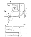
- Figure 1 shows a bridge circuit 10, the first Transistor T1, a second transistor T2, a third Contains transistor T3 and a fourth transistor T4.
- the bridge circuit 10 is one Energy source 13 supplied with electrical energy, the one Has operating voltage U1.
- the positive potential of Energy source 13 leads over a first one Power supply line 14 to the first and third transistor T1, T3.
- the negative potential of the energy source is due to second and fourth transistor T2, T4. Not in the figure the second power supply line is entered, which leads the negative potential.
- a pulse width modulator 15 is used Power specification signal 16 in a pulse width modulated Signal 17 um, which the second transistor T2 immediately as Switching signal is supplied and that via a Drive circuit 18 switches the first transistor T1.
- the power specification signal 16 continues to reach one Comparator 19, the power specification signal 16 with a Limit value 20 compares and depends on Comparison result a switching signal 21 to the Pulse width modulator 15 outputs.
- the control circuit 18 is connected by a pump circuit 22 electrical energy.
- the pump circuit 22 contains one connected to the first power supply line 14 Diode 23, and one connected in series with the diode 23 Pump capacitor 24, the connection point 25 of the first and second transistor T1, T2 is connected to the the load 12 also lies. At the pump capacitor 24 occurs Pump voltage U2, which is the supply voltage of the Control circuit 18 forms.
- Figure 2 shows pulse diagrams as a function of time t.
- the upper and lower picture of Figure 2 shows the pulse width modulated signal 17 in different operating states.
- the ordinate label with Zero "and One " should have the meaning that with a One "is an on state and at one Zero "there is an off state of the respective transistor T1, T2.
- the upper picture of FIG. 2 shows the pulse width modulated signal 17 with a first period P1.
- the first on period D1 is followed by a first off period D2.
- the device according to the invention for operating the load 12 works as follows:
- the power specification signal 16 gives the electrical power with which the load 12 is to be operated.
- the Power specification signal 16 is in the pulse width modulator 15 converted into the pulse width modulated signal 17, which the Turns transistors T1, T2 on and off.
- On the Control of the transistors T3, T4 is not in the following discussed in more detail since they are in the same way as that of the transistors T1, T2 can be realized.
- the first transistor T1 and fourth transistor T4 or the second transistor T2 and the third transistor T3 each driven simultaneously become.
- the transistors T1, T2 connect the Load 12 and the connection point 25 alternately on the positive or negative potential of the energy source 13. Im shown embodiment controls that pulse width modulated signal 17 the second transistor T2 immediately.
- the control circuit 18 must for one Invert the pulse width modulated signal 17, this ensures that not both transistors T1, Conduct T2 simultaneously.
- the duty cycle D1, D2 of the pulse width modulated signal 17 is on Connection point 25 is given an average voltage the load 12 is available.
- the comparator 19 compares the power specification signal 16 with the limit value 20. If the limit value is exceeded the switching signal 21 ensures an extension of the Periods P1, P2 in the pulse width modulator 15.
- the first period P1 the for example, can be set to a value that is above the human hearing limit.
- the first Period P1 is, for example, 50 microseconds, corresponding to 20 kHz.
- the duty cycle TV that above already by the ratio of the duty cycle D1, D3 to Period P1, P2 has been defined, for example can be varied between 0% and 95%.
- D4 result for a proper Operation of the circuit can not be undercut. in the embodiment shown is the minimum Switch-off duration determined by the pump circuit 22.
- the Pump circuit 22 provides the operating voltage U2 Drive circuit 18 ready, the first transistor T1 switches. Depending on the design of the Circuit as well as in particular the choice of the transistor type the requirement may arise that the switching voltage to Switching the first transistor T1 above the Operating voltage U1 must be.
- the pump circuit 22, the this voltage as the pump voltage U2 at the pump capacitor 24 provides, is on potential jumps at the connection point 25 instructed, which do not fall below a minimum duration may without the risk that the pump voltage U2 falls below a permissible value.
- the device according to the invention therefore provides that at Reaching the limit value 20 the first period P1 the second, longer period P2 is changed.
- This Operation can be both continuous and in one stage respectively.
- the limit case with a continuous increase is reached when increasing the Performance target signals 16 above the limit 20 die Switch-off duration D2, D4 does not change and only that Duty cycle D1, D3 is continuously increased.
- Another embodiment sees a step-like increase before, which in extreme cases consists of only one Can increase level.
- This configuration is the Based on the pulse diagram of Figure 2. With one there shown duty cycle of at least approximately 95% is there from the first period P1 to the longer one second period switched, while maintaining the Duty cycle TV of 95%. After exceeding the Limit value 20, the first switch-off duration D2 changes immediately to the longer second switch-off duration D4. Now the duty cycle TV can reach a value of over 95% be increased to a value at which the second Switch-off duration D4 again the minimum permissible value has reached.
- the first period P1 to, for example, 50 microseconds and the second Period P2 can be set to 10 milliseconds with a predetermined minimum switch-off time D2, D4 of 5 Microseconds the duty cycle TV below the limit 20 between 0% and 95% and above the limit 20 can be varied between 95% and 99.95%.
- D2 a predetermined minimum switch-off time
- the duty cycle TV below the limit 20 between 0% and 95% and above the limit 20 can be varied between 95% and 99.95%.
- a Electric motor as a load 12 can be such an extensive either continuous or gradual lowering of the Period P1, P2 to values that are far in human Listening area, can be used without Noise problems occur because the inductive component of the Electric motor with a duty cycle TV above 95% no significant drop in power that allows would cause noisy jumps in moment.
Landscapes
- Engineering & Computer Science (AREA)
- Power Engineering (AREA)
- Amplifiers (AREA)
- Dc-Dc Converters (AREA)
- Electronic Switches (AREA)
Abstract
Description

Claims (6)
- Vorrichtung zum Betreiben einer Last (12), mit einem Impulsbreitenmodulator (15), der in Abhängigkeit von einem Leistungsvorgabesignal (16) die elektrische Leistung durch Variation des Tastverhältnisses (TV) eines impulsbreitenmodulierten Signals (17) festlegt, dadurch gekennzeichnet, daß ein Vergleicher (19) vorgesehen ist, der das Leistungsvorgabesignal (16) mit einem Grenzwert (20) vergleicht und daß die Periodendauer (P1, P2) des impulsbreitenmodulierten Signals (17) bei einer Überschreitung des Grenzwerts (20) verlängert ist.
- Vorrichtung nach Anspruch 1, dadurch gekennzeichnet, daß die Verlängerung der Periodendauer (P1, P2) kontinuierlich erfolgt.
- Vorrichtung nach Anspruch 2, dadurch gekennzeichnet, daß die Ausschaltdauer (D2, D4) des impulsbreitenmodulierten Signals (17) oberhalb des Grenzwerts (20) konstant auf einem minimal vorgegebenen Wert gehalten ist.
- Vorrichtung nach Anspruch 1, dadurch gekennzeichnet, daß die Verlängerung der Periodendauer (P1, P2) des impulsbreitenmodulierten Signals (17) in einer Stufe von einer ersten Periodendauer (P1) auf eine zweite Periodendauer (P2) vorgesehen ist.
- Vorrichtung nach einem der vorhergehenden Ansprüche, dadurch gekennzeichnet, daß das Tastverhältnis (TV) von einer Änderung der Periodendauer (P1, P2) nicht beeinflußt ist.
- Vorrichtung nach einem der vorhergehenden Ansprüche, dadurch gekennzeichnet, daß eine der Last (12) zugeordnete Endstufe (10) einen High-Side-Schalter (T1) sowie eine Pumpschaltung (22) zur Spannungserhöhung enthält und das der Grenzwert (20) auf die Funktionsfähigkeit der Pumpschaltung (20) abgestimmt ist.
Applications Claiming Priority (2)
| Application Number | Priority Date | Filing Date | Title |
|---|---|---|---|
| DE19927903A DE19927903A1 (de) | 1999-06-18 | 1999-06-18 | Vorrichtung zum Betreiben einer Last |
| DE19927903 | 1999-06-18 |
Publications (2)
| Publication Number | Publication Date |
|---|---|
| EP1061637A2 true EP1061637A2 (de) | 2000-12-20 |
| EP1061637A3 EP1061637A3 (de) | 2002-03-27 |
Family
ID=7911713
Family Applications (1)
| Application Number | Title | Priority Date | Filing Date |
|---|---|---|---|
| EP00112367A Withdrawn EP1061637A3 (de) | 1999-06-18 | 2000-06-09 | Vorrichtung zum Betrieben einer Last |
Country Status (2)
| Country | Link |
|---|---|
| EP (1) | EP1061637A3 (de) |
| DE (1) | DE19927903A1 (de) |
Families Citing this family (3)
| Publication number | Priority date | Publication date | Assignee | Title |
|---|---|---|---|---|
| DE102006018149B4 (de) * | 2006-04-19 | 2023-02-09 | Infineon Technologies Ag | Brückenschaltung mit integrierter Ladungspumpe |
| DE102010045292A1 (de) | 2009-10-22 | 2011-04-28 | GM Global Technology Operations, Inc., Detroit | Verfahren für die Steuerung einer Vorrichtung mittels Pulsbreitenmodulation und Steuerungssystem |
| DE102011012849A1 (de) * | 2011-03-03 | 2012-09-06 | Borgwarner Beru Systems Gmbh | Verfahren und Schaltung zum Steuern der Heizleistung einer Heizvorrichtung eines Kraftfahrzeugs |
Family Cites Families (8)
| Publication number | Priority date | Publication date | Assignee | Title |
|---|---|---|---|---|
| US3530353A (en) * | 1967-08-30 | 1970-09-22 | Chicago Aerial Ind Inc | Control circuits for inductive loads |
| IN147639B (de) * | 1977-02-11 | 1980-05-10 | Cableform Ltd | |
| US4479216A (en) * | 1982-12-22 | 1984-10-23 | At&T Bell Laboratories | Skew-free clock circuit for integrated circuit chip |
| US5051880A (en) * | 1989-12-29 | 1991-09-24 | At&T Bell Laboratories | Mixed mode regulation controller for a resonant power converter |
| FI96551C (fi) * | 1993-11-24 | 1996-07-10 | Nokia Telecommunications Oy | Menetelmä ja laite kellosignaalin symmetroimiseksi |
| DE4340769A1 (de) * | 1993-11-30 | 1995-06-01 | Bosch Gmbh Robert | Verfahren und Vorrichtung zur Steuerung elektrischer Geräte mittels einer Pulsweitenmodulations-Einrichtung |
| DE19506273A1 (de) * | 1995-02-23 | 1996-09-05 | Telefunken Microelectron | Schaltungsanordnung zur Steuerung von drehzahlveränderlichen DC-Motoren |
| US5739658A (en) * | 1995-03-31 | 1998-04-14 | International Business Machines Corporation | Noise dithering system for transistor switched devices |
-
1999
- 1999-06-18 DE DE19927903A patent/DE19927903A1/de not_active Ceased
-
2000
- 2000-06-09 EP EP00112367A patent/EP1061637A3/de not_active Withdrawn
Also Published As
| Publication number | Publication date |
|---|---|
| EP1061637A3 (de) | 2002-03-27 |
| DE19927903A1 (de) | 2000-12-28 |
Similar Documents
| Publication | Publication Date | Title |
|---|---|---|
| EP0739084B1 (de) | Verfahren zum Steuern oder Regeln eines Elektromotors, und Anordnung zur Durchführung eines solchen Verfahrens | |
| DE60212818T2 (de) | Regelungsvorrichtung und verfahren für einen gleichstrom/gleichstrom-wandler | |
| DE4126291C2 (de) | Wechselrichter mit Treiberkreisen und deren Speisung nach dem Ladungspumpen-Prinzip | |
| DE4419006A1 (de) | Pulsweitenmodulierter Schaltwandler zum Betrieb elektrischer Verbraucher | |
| DE9409760U1 (de) | Schaltungsanordnung zur Ansteuerung eines Schützes | |
| DE3346435A1 (de) | Schaltungsanordnung zum ein- und ausschalten sowie zum ueberwachen elektrischer verbraucher | |
| DE69009122T2 (de) | Aufwärts und abwärts Zerhacker. | |
| EP2129897B1 (de) | Ansteuerschaltung und ansteuerverfahren für ein piezoelektrisches element | |
| EP1658676B1 (de) | Schaltung und verfahren zum verarbeiten einer speisespannung mit spannungsspitzen | |
| DE69803885T2 (de) | Steuerungsvorrichtung für elektrische motoren | |
| DE69220456T2 (de) | Schaltungsanordnung | |
| WO2002015374A1 (de) | Schaltungsanordnung und elektrogerät mit einer induktiven last und einem drosselwandler | |
| DE2506196C2 (de) | Gleichstrom-Schaltvorrichtung zur Erhöhung des Spitzenstromes | |
| DE4008663C1 (de) | ||
| EP1061637A2 (de) | Vorrichtung zum Betrieben einer Last | |
| EP1031182A2 (de) | Verfahren und schaltungsanordnung zur erzeugung eines pulsbreitenmodulierten stellsignals für einen gleichstromaktuator | |
| DE3238127A1 (de) | Anordnung zur steuerung von halbleiterschaltungen | |
| EP1532726B1 (de) | Schaltregler | |
| EP1427095A2 (de) | Elektronisch kommutierter Elektromotor | |
| DE60013681T2 (de) | Ein Gleichspannungswandler mit mehrere Ausgängen, insbesondere zum Betrieb in Fahrzeugen | |
| DE102020111167B4 (de) | Leistungsaufnahmereduktion einer Relaisschaltung für Elektrofahrzeuge bei hohen Betriebsspannungen | |
| EP0353533A1 (de) | Schaltungsanordnung bei Endstufen für die Steuerung von Stellmagneten | |
| DE9302756U1 (de) | Rückkopplungsregler | |
| EP1609236B1 (de) | Verfahren und steuereinheit zur ansteuerung von lüftermotoren | |
| DE3914287A1 (de) | Gleichspannungswandler |
Legal Events
| Date | Code | Title | Description |
|---|---|---|---|
| PUAI | Public reference made under article 153(3) epc to a published international application that has entered the european phase |
Free format text: ORIGINAL CODE: 0009012 |
|
| AK | Designated contracting states |
Kind code of ref document: A2 Designated state(s): AT BE CH CY DE DK ES FI FR GB GR IE IT LI LU MC NL PT SE Kind code of ref document: A2 Designated state(s): DE ES FR GB IT |
|
| AX | Request for extension of the european patent |
Free format text: AL;LT;LV;MK;RO;SI |
|
| PUAL | Search report despatched |
Free format text: ORIGINAL CODE: 0009013 |
|
| AK | Designated contracting states |
Kind code of ref document: A3 Designated state(s): AT BE CH CY DE DK ES FI FR GB GR IE IT LI LU MC NL PT SE |
|
| AX | Request for extension of the european patent |
Free format text: AL;LT;LV;MK;RO;SI |
|
| RIC1 | Information provided on ipc code assigned before grant |
Free format text: 7H 02M 3/158 A, 7H 02P 7/29 B |
|
| 17P | Request for examination filed |
Effective date: 20020927 |
|
| AKX | Designation fees paid |
Free format text: DE ES FR GB IT |
|
| 17Q | First examination report despatched |
Effective date: 20090507 |
|
| GRAP | Despatch of communication of intention to grant a patent |
Free format text: ORIGINAL CODE: EPIDOSNIGR1 |
|
| INTG | Intention to grant announced |
Effective date: 20140827 |
|
| STAA | Information on the status of an ep patent application or granted ep patent |
Free format text: STATUS: THE APPLICATION IS DEEMED TO BE WITHDRAWN |
|
| 18D | Application deemed to be withdrawn |
Effective date: 20150106 |