EP1061691A2 - Digitale PLL-Schaltung für Burstbetrieb und optische Empfangsschaltung, die dieselbe verwendet - Google Patents
Digitale PLL-Schaltung für Burstbetrieb und optische Empfangsschaltung, die dieselbe verwendet Download PDFInfo
- Publication number
- EP1061691A2 EP1061691A2 EP00111934A EP00111934A EP1061691A2 EP 1061691 A2 EP1061691 A2 EP 1061691A2 EP 00111934 A EP00111934 A EP 00111934A EP 00111934 A EP00111934 A EP 00111934A EP 1061691 A2 EP1061691 A2 EP 1061691A2
- Authority
- EP
- European Patent Office
- Prior art keywords
- burst
- mode data
- circuit
- signal
- clock
- Prior art date
- Legal status (The legal status is an assumption and is not a legal conclusion. Google has not performed a legal analysis and makes no representation as to the accuracy of the status listed.)
- Withdrawn
Links
Images











Classifications
-
- H—ELECTRICITY
- H04—ELECTRIC COMMUNICATION TECHNIQUE
- H04L—TRANSMISSION OF DIGITAL INFORMATION, e.g. TELEGRAPHIC COMMUNICATION
- H04L7/00—Arrangements for synchronising receiver with transmitter
- H04L7/02—Speed or phase control by the received code signals, the signals containing no special synchronisation information
- H04L7/033—Speed or phase control by the received code signals, the signals containing no special synchronisation information using the transitions of the received signal to control the phase of the synchronising-signal-generating means, e.g. using a phase-locked loop
- H04L7/0337—Selecting between two or more discretely delayed clocks or selecting between two or more discretely delayed received code signals
-
- H—ELECTRICITY
- H04—ELECTRIC COMMUNICATION TECHNIQUE
- H04L—TRANSMISSION OF DIGITAL INFORMATION, e.g. TELEGRAPHIC COMMUNICATION
- H04L7/00—Arrangements for synchronising receiver with transmitter
- H04L7/04—Speed or phase control by synchronisation signals
Definitions
- the present invention relates to digital phase locked loop circuits (hereinafter, PLL circuits), and more specifically to a digital PLL circuit recovering a clock signal according to received burst-mode data, and adjusting a phase thereof in such a manner as to synchronize with an optimal position of each bit of the burst-mode data.
- PLL circuits digital phase locked loop circuits
- a center station In a point-to-multipoint network where a center station is connected to a plurality of terminals, two-way data communication is carried out among the terminals in which frequency synchronization is established. On reception of data from the terminals, the center station determines a phase thereof and then recovers a clock based on the determined phase so that the received data is recovered.
- Such data recovery is exemplarily found in ISSCC '93 TA6.4 (hereinafter, first conventional example).
- a reception terminal first instantaneously determines a phase of received data; recovers a clock; and discriminates the received data according to the recovered clock.
- a first and a second Voltage Controlled Oscillators are utilized therefor, and are structured to oscillate responding to a gate signal.
- An oscillating frequency of the first and second VCOs is synchronized with that of a system clock.
- the second VCO When the received data transits from “Low” to "High”, the second VCO then stops oscillating. Accordingly, the first VCO keeps oscillating as long as the received data indicates "High", and the second VCO "Low". A logical sum of output signals from the first and second VCOs is regarded as a clock recovered based on the received data.
- burst-mode data which is the received data. If the distortion is fully suppressed, a falling edge (tail) of the recovered clock correctly comes to the center of each bit. Accordingly, the received burst-mode data is sampled utilizing the falling edge and then correctly discriminated.
- the burst-mode data may not be correctly discriminated in some cases. For instance, if a bit indicating "High" is narrowed in width to about half due to the pulse width distortion, the burst-mode data may not be correctly sampled utilizing the falling edge of the recovered clock.
- the first and second VCOs may not be equalized to a preset system clock in oscillating frequency, or an error in oscillating frequency may be generated thereamong due to noise, for example. If data is recovered under such circumstance, a phase of the recovered clock may move off, by degrees, from a centric position of the bit during continuity of bits indicating the same level ("High or "Low”). It may result in erroneous discrimination of the burst-mode data.
- the third conventional example is a technique disclosed in Japanese Patent Laying-Open No. 8-237117 (96-237117).
- an average in position is taken for falling edges of received data, and an optimal phase position is determined based on information about the average.
- the number of transition points is detected in one-bit width, where the optimal phase position is centered.
- two transition points therein mean that pulse width distortion and/or jitter is occurred in the received data.
- a center value of these two transition points is taken as optimal phase position, and thus an influence of pulse width distortion and/or jitter is prevented for discrimination of the received data.
- one or no transition point means that the received data has no pulse width distortion. Therefore, the optimal phase position remains the same.
- the average is calculated for the transition points in several bits before selecting the optimal phase position.
- the problem herein is, the average may be calculated including transition points erroneously detected in a non signal period.
- the non signal period is an interval where a circuit utilizing the second and third conventional examples do not receive data, and supposedly no data is sent out from an AGC amplifier preceding to the circuit in the non signal period.
- Such erroneous detection is caused by noise to be occurred therein as the noise is mistakenly regarded as randomly-generated data.
- recovery for a clock having a correct phase position cannot be done in the vicinity of a head of the burst-mode data (that is, at the beginning of a signal period, which is located after the non signal period and data reception is made therein).
- a comparator in the last stage of the AGC amplifier is provided with a hysteresis function, whereby an output signal of the AGC amplifier is fixedly set to "0" when there is no burst-mode data (non signal period).
- a reference signal shifts in value with respect to an incoming signal depending on an output from the comparator. Accordingly, the AGC amplifier can output a signal indicating "0" in level without amplifying the noise occurred in the non signal period.
- the hysteresis function lowers an SN ratio (Signal to Noise Ratio), in other words, a reception level for high-quality data communication with a low bit error rate suffers deterioration.
- the hysteresis function may cause no problem if the reference signal can be kept at the same shifting level to both output signals indicating "0" and "1". If it is impossible due to variation of devices realizing the hysteresis function, the comparator problematically enhances the pulse width distortion before outputting a signal.
- a fourth conventional example is a data sheet of Lucent Technologies, titled "20Mb/s-60Mb/s Burst-Mode Clock and Data Recovery Integrated Circuit ATTDC221AJ32".
- the system shown in the data sheet is similar to the first conventional example, but the data recovery circuit therein is additionally provided with an elastic buffer.
- received data is written according to a recovered clock. Reading from the elastic buffer is carried out utilizing a clock in the data recovery circuit, and thus the received data becomes free from uttering components.
- a reset signal is provided immediately before receiving the burst-mode data. With the reset signal, the data recovery circuit adjusts timing for reading from the elastic buffer when writing is started, whereby reading is secured not to start before writing.
- the problem in the fourth conventional example is that the clock is erroneously recovered due to noise occurred in the non signal period, and according to the erroneous clock recovered thereby, data is written into the elastic buffer. As a result, a writing position of data may be shifted from a preset position, and a writing position of data thus comes before the reading position. Due to such problem, for the worst, new data is overwritten in a not-yet-read data region, whereby data cannot be correctly read.
- an object of the present invention is to provide a digital PLL circuit for correctly discriminating burst-mode data from noise possibly included in a non signal period, and correctly recovering only the burst-mode data from the head thereof.
- Another object of the present invention is to provide an optical receiving circuit for correctly receiving and recovering an optical burst-mode signal without a hysteresis function in a stage subsequent to an AGC amplifier.
- the present invention has the following features to attain the objects above.
- a first aspect of the present invention is directed to a digital PLL circuit recovering a clock signal according to received burst-mode data, and adjusting a phase thereof in such a manner as to synchronize with an optimal position of each bit of the burst-mode data, the circuit comprising:
- the preamble detector detects the head of the burst-mode data. Therefore, the digital PLL circuit can correctly discriminate between the burst-mode data and any interval having the burst-mode data not transmitted.
- the clock phase adjuster detects the recently optimal phase position according to the edge positions of the burst-mode data. In this manner, even if the burst-mode data has pulse width distortion and/or jitter therein, the clock phase adjuster keeps locating the phase of the clock signal onto the optimal phase position with reference to the edge positions of the burst-mode data. Accordingly, the burst-mode data can correctly be discriminated.
- the clock signals having different phases one another are generated according to a system clock, whereby synchronization in frequency between the system clock and the clock signals having different phases one another can be established easily and accurately. Since the clock signals are thus suppressed in frequency variation, the edge of the clock signal always comes to the center of each bit of the burst-mode data even if the burst-mode data has continuity of bits indicating the same level. Therefore, the data can be correctly discriminated.
- the clock phase adjuster in the first aspect, the clock phase adjuster
- the phase positions of the clock signals are adjusted according to the average taken for x evaluation values. Therefore, jittering components are removed from the burst-mode data, and can be recovered by the clock signals always having the optimal phase position.
- the clock phase adjuster detects the edge positions of the burst-mode data from the 1 st to n th sampled burst-mode data generated by the sampling circuit.
- the clock phase adjuster starts operating when the head of the burst-mode data is detected. In this manner, the phase positions of the clock signals are prevented from being erroneously detected in the non signal period of the burst-mode data. As a result, the burst-mode data can be discriminated with higher accuracy.
- the burst-mode data previously has an identification pattern set for specifying the head thereof, and
- n decoders each independently operate to find the identification pattern from the 1 st to n th sampled burst-mode data.
- the head of the burst-mode data can be correctly specified, and thus the digital PLL circuit is prevented from erroneously operating due to confusion between the noise occurred in the non signal period and the burst-mode data. Accordingly, the digital PLL circuit can correctly discriminate between the noise in the non signal period and the burst-mode data.
- the number of bits i held by each of the shift registers is predetermined, wherein
- the decoders determine pattern matching by using bits as many as possible ( j bits), whereby the head of the burst-mode data can be detected with accuracy.
- the identification pattern detector decides that the head of the burst-mode data is detected, wherein
- the decoders can also determine pattern matching with bits fewer in number ( k bits) while satisfying sufficiently-high transmission quality. Therefore, the head of the burst-mode data can swiftly be detected.
- the preamble detector further includes an initial phase position detector detecting a center point of bits at the head of the burst-mode data from the result determined by the n decoders, and determining the detected center point as the optimal phase position for the clock signals.
- the decoders After detected the identification pattern, the decoders can specify the clock signal whose phase position is useful for discriminating the burst-mode data. Therefore, if a plurality of decoders detect the identification pattern, the number of such useful phase positions are also plural.
- the identification phase position detector detects the optimal phase position for these clock signals. Therefore, the digital PLL circuit can recover the clock signal having the optimal phase position for discrimination of the burst-mode data.
- the clock phase adjuster includes an edge detector detecting the edge positions of each bit of the burst-mode data, wherein
- the decision circuit determines whether or not continuity of the same level is observed after detected any transition point in the exclusive OR circuit. In this manner, it prevents the decision circuit from detecting any level change possibly resulted from the noise as the transition point resulted from the burst-mode data.
- the clock phase adjuster stops adjusting the phase positions according to any transition points resulted from the noise, and thus the phase of the clock signal can always be adjusted to be on the correct position.
- the digital PLL circuit further comprises a discriminator discriminating, based on the phase positions adjusted by the clock phase adjuster, a bit to be received from the 1 st to n th sampled burst-mode data generated by the sampling circuit.
- the discriminator operates with timing according to the optimally-adjusted phase position, whereby the bit to be received can be correctly discriminated.
- the elastic buffer absorbs the uttering components. Therefore, the bits (burst-mode data) read from the elastic buffer can be freed from the jitter components.
- writing and reading into/from the elastic buffer are done when the preamble detector detects the head of the burst-mode data.
- a thirteenth aspect of the present invention is directed to an optical receiving circuit receiving an optical burst-mode signal, comprising:
- the value of the reference signal is set to be equal to the reference value of the electrical signal. Accordingly, the comparator can carry out comparison processing with the reference signal in the optimal level, whereby the recovered burst-mode data can be fully suppressed with pulse width distortion. Further, the comparator carries out the comparison processing with the reference signal in a value being offset the reference value by a given value in the non signal period, whereby the noise component is not erroneously recovered as the burst-mode data.
- the electrical signal provided to the comparator is a bi-phase signal.
- the bi-phase signal varying in level in both directions of positive and negative with respect to the reference signal is inputted. Therefore, even if an optical power of receiving signal is low in the signal period, the comparing circuit can correctly carry out the comparison processing as long as the reference signal is set equal to the electrical signal.
- the given value is adequately provided with an allowance for the distribution value of the thermal noise component.
- the comparing circuit is prevented from erroneously recovering the noise component in the non signal period as the burst-mode data.
- the digital PLL circuit comprises:
- the clock phase adjuster in the eighteenth aspect, the clock phase adjuster
- the clock phase adjuster when received the PREAMBLE-DETECTED signal from the preamble detector, starts detecting the edge positions of the burst-mode data outputted from the comparing circuit utilizing the 1 st to n th sampled burst-mode data generated by the sampling circuit.
- the burst-mode data outputted from the comparing circuit previously has an identification pattern set for specifying the head thereof, and
- the number of bits i held by each of the shift registers is predetermined, wherein
- a series of q (where q is a natural number satisfying q ⁇ n ) decoders determine that a pattern of recent k bits (where k is a natural number satisfying k ⁇ j ) out of the i bits held by each corresponding shift register matches to the identification pattern, the identification pattern detector decides that the identification pattern is detected, wherein
- the preamble detector further includes an initial phase position detector estimating a center point of bits in the identification pattern using the result determined by the n decoders, and regarding the estimated center point as the optimal phase position for the clock signals.
- the optical receiving circuit further comprises a discriminator discriminating, based on the phase positions adjusted by the clock phase adjuster, a bit to be received from the 1 st to n th sampled burst-mode data generated by the sampling circuit.
- the discriminator includes:
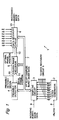
- FIG. 1 Depicted in FIG. 1 is a block diagram showing the structure of a digital PLL circuit 1 according to a first embodiment of the present invention.
- the digital PLL circuit 1 is provided with a clock generator 2, a sampling circuit 3, a preamble detector 4, a clock phase adjuster 5, and a data recovery circuit 6.
- the clock generator 2 is supplied with a system clock clk S , a phase of which is ⁇ s .
- the clock generator 2 then shifts the n -branched system clocks clk S in phase, preferably in a uniform manner, and thus n clock signals clk 1 to clk n are generated.
- phase positions of the clock signals clk 1 to clk n are ⁇ 1 to ⁇ n
- phase positions ⁇ 1 to ⁇ n are respectively at an edge (in this embodiment, leading edge) of the clock signals clk 1 to clk n .
- These clock signals clk 1 to clk n are forwarded to both the sampling circuit 3 and the data recovery circuit 6.
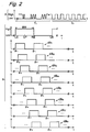
- the digital PLL circuit 1 in FIG. 1 is supplied with intermittently-generating digital data (hereinafter, burst-mode data). As shown in FIG. 2A, a non signal period T 1 is observed before and after a signal period T 2 .
- the non signal period T 1 is a time interval having no burst-mode data transmitted, and the signal period T 2 having the burst-mode data transmitted.
- burst-mode data is provided to the sampling circuit 3 through a signal line 9.
- the sampling circuit 3 is also provided with the clock signals clk 1 to clk n from the clock generator 2.
- the sampling circuit 3 After branching the received burst-mode data into n , the sampling circuit 3 samples the n -branched burst-mode data utilizing the clock signals clk 1 to clk n (see FIG. 2B), and thus 1 st to n th sampled burst-mode data is generated.
- the 1 st to n th sampled burst-mode data is transmitted, through a data bus 7, to the preamble detector 4, the clock phase adjuster 5, and the data recovery circuit 6, respectively.
- the preamble detector 4 detects a head of the 1 st to n th sampled burst-mode data, and then the optimal position ⁇ OPT for the detected head. Thereafter, the preamble detector 4 transmits information specifying the detected optimal phase position ⁇ OPT (hereinafter, INITIAL PHASE POSITION) to the clock phase adjuster 5 through a bus 11.
- the center point CP of each bit may vary with time due to possibilities for pulse width distortion or jitter superimposed on the burst-mode data. Therefore, although the INITIAL PHASE POSITION surely indicates the optimal phase position ⁇ OPT at the head of the burst-mode data, there is no assurance therefor after a lapse in time.
- the clock phase adjuster 5 starts operation, and then so adjusts that the optimal phase position ⁇ OPT follows the time-varying center point CP of each bit. Specifically, immediately after start-up, the clock phase adjuster 5 receives both INITIAL PHASE POSITION through the bus 11 and the 1 st to n th sampled burst-mode data through the data bus 7. The clock phase adjuster 5 then transmits the optimal phase position ⁇ OPT indicated by the received INITIAL PHASE POSITION as an OPTIMAL PHASE POSITION, without any change, to the data recovery circuit 6 through a bus 12.
- the clock phase adjuster 5 finds the recently optimal phase position ⁇ OPT among ⁇ 1 to ⁇ n , and then transmits the OPTIMAL PHASE POSITION as information indicating the recently optimal phase position ⁇ OPT to the data recovery circuit 6 through the bus 12. From then and onwards, the clock phase adjuster 5 repeats the operation of generating and transmitting the OPTIMAL PHASE POSITION indicating the recently optimal phase position ⁇ OPT .
- the data recovery circuit 6 In response to the PREAMBLE-DETECTED signal, the data recovery circuit 6 starts operation, and then recovers the burst-mode data. Immediately after start-up, the data recovery circuit 6 receives both the OPTIMAL PHASE POSITION through the bus 12 and the 1 st to n th sampled burst-mode data through the data bus 7. Further, the data recovery circuit 6 receives the clock signals clk 1 to clk n generated by the clock generator 2. The data recovery circuit 6 recovers the received 1 st to n th sampled burst-mode data, and then writes a bit string into an internal elastic buffer 64 (see FIG. 17).
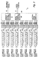
- FIG. 3 shows the detailed structure of the preamble detector 4 in FIG. 1.
- the preamble detector 4 includes 8 shift registers 41 1 to 41 8 , 8 decoders 42 1 to 42 8 , and a pattern/initial phase detector 43.
- the shift registers 41 1 to 41 8 each have the capacity for 7 bits.
- the shift register 41 1 holds a series of 7 bits in the 1 st sampled burst-mode data for output to the decoder 42 1 .
- the shift registers 41 2 to 41 8 are similar in function to the shift register 41 1 , and differed only in a respect in outputting a series of 7 bits in the 2 nd to 8 th sampled burst-mode data respectively to the decoders 42 2 to 42 8 . Therefore, the shift registers 41 2 to 41 8 are not described.
- the decoders 42 2 to 42 8 are similar in function to the decoder 42 1 , and differed only in a respect in carrying out processing as described above based on the series of 7 bits from the shift registers 41 2 to 41 8 . Therefore, the decoders 42 2 to 42 8 are not described.
- the pattern/initial phase detector 43 includes an identification pattern detector 44, which generates, with the received decoding results, a PREAMBLE-DETECTED signal which is a signal indicating the detection of the head of the burst-mode data for output to the signal line 10.
- the pattern/initial phase detector 43 also includes an initial phase position detector 45, which detects, with the decoding results, the optimal phase position ⁇ OPT among the phase positions ⁇ 1 to ⁇ 8 for discrimination of the head of the burst-mode data provided to the digital PLL circuit 1.
- the initial phase position detector 45 outputs the detected optimal phase position ⁇ OPT to the bus 11 as an INITIAL PHASE POSITION.
- the identification pattern detector 44 is described in detail by referring to FIGS. 4 to 6, and the like, and then the initial phase position detector 45 is described in detail by referring to FIG. 7, and the like.
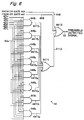
- the identification pattern detector 44 includes 8 AND gates 441 1 to 441 8 , an OR gate 443, 8 AND gates 445 1 to 445 8 , an OR gate 447, 8 AND gates 449 1 to 449 8 , and OR gates 4411 and 4413.
- the OR gate 4411 performs logical operation with respect to the results obtained from the AND gates 449 1 to 449 8 through the signal lines 4410 1 to 4410 8 for output to a signal line 4412.
- the OR gate 4413 is provided with the results of the OR gates 443, 447, and 4411 through the signal lines 444, 448, and 4412.
- the OR gate 4413 performs logical operation with respect to the results, and then outputs a result obtained thereby as a PREAMBLE-DETECTED signal.
- the burst-mode data provided to the digital PLL circuit 1 may have pulse width distortion and/or jitter. Such pulse width distortion and/or jitter may cause the preset one-bit width BW of the burst-mode data to vary with time.
- the shift registers 41 1 to 41 8 each have the capacity for 7 bits (equivalent to a natural number i in claims), and why the number of bits (equivalent to j or k in claims) for the decoders 42 1 to 42 8 to handle is 5 to 7. The description is made for a case where the one-bit width BW varies in a range of 5/8 to 11/8 compared with a preset (value).
- the digital PLL circuit 1 receives randomly-generated data varied in level between "High” and "Low”. Therefore, if the sampling circuit 3 samples such randomly-generated data utilizing the clock signals clk 1 to clk 8 (see FIG. 2B), a signal to be outputted therefrom as 1 st to 8 th sampled burst mode data may have a 50/50 (0.5) possibility for "High” or "Low”.
- the AND gate 441 1 in FIG. 4 is now referred to.
- the value obtained by the equation (1) is also a probability for the AND gate 441 1 outputting "High".
- a probability for any one of the AND gates 441 1 to 441 8 , the AND gates 445 1 to 445 8 , and the AND gates 449 1 to 449 8 outputting "High", i.e., a probability for a PREAMBLE-DETECTED signal indicating "High” is denoted by Pe 1 , Pe 2 , and Pe 3 .
- the probabilities Pe 1 , Pe 2 , and Pe 3 each denote a probability for erroneously detecting, as the head of the burst-mode data, an incoming signal whose value is invariable.
- the probabilities Pe 1 , Pe 2 , and Pe 3 are regarded as being sufficiently small. Therefore, even if any bit error is caused in the digital PLL circuit 1 due to the erroneous detection of the head, the preamble detector 4 shows no problem for practical use.
- the head of the incoming burst-mode data can be swiftly detected.
- simply using bits fewer in number leads to a higher probability for erroneously detecting the head of the burst-mode data.
- the number (equivalent to q in claims) of the decoders 42 (i.e., shift registers 41) to be coupled to the AND gates 445 b or 449 b is increased.
- an expression of "a series of q decoders" in claims means q decoders 42 receiving 1 st to q th sampled burst-mode data (obtained by sampling the input burst-mode signal utilizing q clock signals clk b in a row).
- the initial phase position detector 45 is described in detail with reference to FIG. 7.
- the initial phase position detector 45 is provided with the results obtained by the AND gates 441 1 to 441 8 . 445 1 to 445 8 , and 449 1 to 449 8 through the signal lines 442 1 to 442 8 , 446 1 to 446 8 , and 4410 1 to 4410 8 .
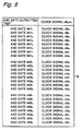
- the initial phase position detector 45 operates in accordance with a predetermined rule ⁇ (see FIG. 8) so as to detect a clock signal clk OPT having the optimal phase position ⁇ OPT .
- the clock signal clk OPT is any one of the clock signals clk 1 to clk 8 .
- the rule ⁇ in FIG. 8 is set as described next below.
- the one-bit width BW and the phase differential ⁇ are both known.
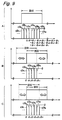
- FIG. 9B even if jitter is occurred in the bits of the burst-mode data, the bits cover at least the phase positions ⁇ 1 to ⁇ 5 .
- the clock signal clk 3 thus has the highest possibility for coming to the center point CP of each bit. If this is the case, as shown in FIG. 8, with the AND gate 441 1 outputting "High", the clock signal clk 3 is selected.
- the initial phase position detector 45 specifies the clock signal clk OPT being in closest vicinity to the center point CP of each bit.
- the initial phase position detector 45 generates a value indicating the specified clock signal clk OPT for transmission to the clock phase adjuster 5 (see FIG. 11) as an INITIAL PHASE POSITION.
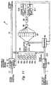
- the clock phase adjuster 5 includes an optimal phase holder 51, an edge detector 52, 7 registers 53 1 to 53 7 , a selector 54, an address controller 55, a counter 56, a register 57, an adder 58, a divider 59, an up-pulse generation part 510, and a down-pulse generation part 511.
- phase position ⁇ OPT (i.e., the clock signal clk OPT ) specified by the INITIAL PHASE POSITION is obtained from the head of the incoming burst-mode data. Therefore, although the phase position ⁇ OPT is initially valid, there is no assurance therefor after a lapse in time. This is because pulse width distortion and/or jitter causes the center point CP of each bit to vary with time. To get around such problem, the clock phase adjuster 5 have the optimal phase position ⁇ OPT come to the center point CP of each bit.
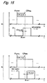
- the edge detector 52 detects, according to the 1 st to 8 th sampled burst-mode data transmitted through the data bus 7, an edge position ⁇ EDGE at the front edge LE (leading edge) or the rear edge RE (falling edge) of each bit.
- the detected edge position ⁇ EDGE is transmitted to the selector 54 and the counter 56 as an EDGE POSITION through a bus 512.
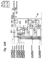
- the edge detector 52 has such structure as shown In FIG. 12.
- the edge detector 52 includes 8 exclusive OR circuits 521 1 to 521 8 , 8 decision circuits 522 1 to 522 8 , 8 AND gates 523 1 to 523 8 , and D-type flip-flop amplifiers 524 1 to 524 8 .
- the exclusive OR circuit 521 b detects two types of transition points.
- the first transition point is the one resulted from the leading edge LE and the falling edge FE, and indicates an edge position necessary for the clock phase adjuster 5.
- the leading edge LE of each bit is located between the phase positions ⁇ 1 and ⁇ 2 .
- the exclusive OR circuit 521 1 outputs "High" but not others.
- the AND gate 523 b determines that the transition point between the phase positions ⁇ 1 and ⁇ 2 is not resulted from the leading edge LE or the falling edge FE but the noise (see arrow ⁇ ).
- the combination of the AND gate 521 b , the decision circuit 522 b , and the AND gate 523 b makes it possible to detect only the first transition point resulted from the leading edge LE or the falling edge FE.
- the values held by the flip-flop amplifiers 524 1 to 524 8 are transmitted with the same timing and are superimposed on the bus 512.
- an EDGE POSITION having an 8-bit width is generated.
- the EDGE POSITION specifies the edge position ⁇ EDGE as any one of the phase positions ⁇ 1 to ⁇ 8 . In the case in FIG. 13A, only the flip-flop amplifier 524 1 outputs "High” and others "Low”. Accordingly, the EDGE POSITION indicates (Hi, Lo, Lo, Lo, Lo, Lo, Lo). If this is the case, the edge position ⁇ EDGE is between the phase positions ⁇ 1 and ⁇ 2 .
- the previous phase position ⁇ OPT ' is the phase position judged as being in the closest vicinity to the center point CP of each bit of the incoming burst-mode data in the last processing.
- the previous phase position ⁇ OPT ' may move off from the center point CP of each bit with a lapse in time.
- the address controller 55 receives the evaluation value and the count value. To a stage subsequent thereto, the register 57 which can hold the evaluation value for x words (equivalent to x in claims) is coupled. To a region in which a unit word is stored, unique addresses "1" to "x" are each assigned. The address controller 55 writes the received evaluation value to an address of the register 57 indicated by the received count value.
- the evaluation value is sequentially written into the register 57 every time the edge position ⁇ EDGE of each bit is detected.
- the adder 57 receives the evaluation value for x words from the register 57 so as to calculates a total thereof. Thereafter, the divider 59 divides the total by x. The average is thus taken for x-piece of evaluation values.
- the calculated average is forwarded to the up-pulse generation part 510 and the down-pulse generation part 511.
- the up-pulse generation part 510 outputs an up-pulse to the optimal phase holder 51 only when the average is equal to or larger than "+1".
- the down-pulse generation part 511 outputs a down-pulse to the optimal phase holder 51 only when the average is equal to or smaller than "-1".
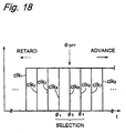
- the up-pulse and down-pulse each indicate that the center points CP PRE detected for x times are averagely advanced or retarded with respect to the previous optimal phase position ⁇ OPT '.
- the optimal phase holder 51 Based on the received up-pulse or down-pulse, the optimal phase holder 51 generates a value indicating the recent optimal position ⁇ OPT , and holds the value as a new OPTIMAL PHASE POSITION.
- the up-pulse provided as shown in FIG. 16B, the position retarded from the previous optimal position ⁇ OPT ' by one phase differential ⁇ is selected as the recent optimal phase position ⁇ OPT .
- the recent optimal phase position ⁇ OPT is, as shown in FIG. 16A, advanced from the previous optimal phase position ⁇ OPT , by one phase differential ⁇ .
- Such new OPTIMAL PHASE POSITION is forwarded to the data recovery circuit 6 through the bus 12.
- the selector 61 selects clock signals clk (b-1) to clk (b+1) whose phase positions are ⁇ (b-1) to ⁇ (b+1) . Then, the selector 61 selects only (b-1) th to (b+1) th sampled burst-mode data obtained by sampling utilizing the clock signals clk (b-1) to clk (b+1) for output to the decision circuit 62.
- the pointer controller 63 receives the PREAMBLE-DETECTED signal, the OPTIMAL PHASE POSITION, and the clock signals clk 1 to clk 8 having different phases one another. In response to the PREAMBLE-DETECTED signal, the pointer controller 63 starts operation. After start-up, the pointer controller 63 selects, out of the clock signals clk 1 to clk 8 , the clock signal clk b having the optimal phase position ⁇ OPT (that is, ⁇ b ) indicated by the OPTIMAL PHASE POSITION.
- the decision circuit 62 determines which bit (level "High” or "Low”) is to be written into the subsequent elastic buffer 64. For example, when the (b-1) th , the b th , and the (b+1) th sampled burst-mode data respectively indicate High”, “Low", and “High”, "High” is more in number than "Low”. Accordingly, the level "High” is discriminated as a to-be-written bit (burst-mode data). Thereafter, the decision circuit 62 writes the discriminated bit (burst-mode data) to the elastic buffer 64 in an address indicated by the first count value provided from the pointer controller 63. Further, since the first count value is synchronized with the clock signal clk b , writing into the elastic buffer 64 is carried out in synchronization with the clock signal clk b .
- the decision circuit 62 is not structurally essential for the digital PLL circuit 1. However, the decision circuit 62 is preferably incorporated thereinto as it improves the resistance to noise possibly occurring in the burst-mode data provided to the digital PLL circuit 1. Next below, it is described how the noise resistance is improved.
- the discriminator 66 writes only the b th sampled burst-mode data selected by the selector 61 into the elastic buffer 64. In this manner, the object (discriminate between the non signal period and burst-mode data so as to correctly recover only the burst-mode data) of the digital PLL circuit 1 can be achieved.
- the randomly-occurring noise may superimpose on the optimal phase position ⁇ OPT ( ⁇ b ) of the burst-mode data. If this is the case, the b th sampled burst-mode data obtained by sampling utilizing the clock signal clk b (phase position ⁇ b ) may have a bit error.
- Some noise may be instantaneously superimposed on the burst-mode data. Such noise, however, may be superimposed on the phase position ⁇ b but not on the phase positions ⁇ (b-1) and ⁇ (b+1) in the vicinity thereof. It means that the (b-1) th and (b+1) th sampled burst-mode data barely has a bit error.
- the decision circuit 62 takes majority for the (b-1) th to (b+1) th sampled burst-mode data selected by the selector 61. Therefore, with the decision circuit 62 incorporated, the bit to be written into the elastic buffer 64 is decreased in possibility for any noise-caused error. As a result, the resistance to noise possibly occurring in the burst-mode data can be improved.
- the pointer controller 63 outputs not only the first count value but the second. It is now described how the pointer controller 63 operates to output the second count value. Any one of the clock signals clk 1 to clk 8 provided to the pointer controller 63 is equal to the system clock clk S in phase position ⁇ S .
- the pointer controller 63 synchronizes with the system clock clk S (phase position ⁇ S ), and then increments the second count value for output to the reading circuit 65.
- the second count value indicates a reading address from the elastic buffer 64 (later described).
- the reading circuit 65 reads the burst-mode data written into the elastic buffer 64 from the address indicated by the second count value provided by the pointer controller 63. Since the second count value is synchronized with the system clock clk S , reading from the elastic buffer 64 is carried out also in synchronization with the system clock clk S . Note that, an initial value of the writing address of the decision circuit 62 and that of the reading address of the reading circuit 65 are previously so set as to be logically furthermost to each other in the address region of the elastic buffer 64. The reading circuit 65 outputs the read bit string to the signal line 13 as the recovered burst-mode data.
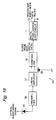
- the optical receiving circuit 14 includes an optical/electrical conversion device 15, a preamplifier 16, a linear amplifying circuit 17, a reference signal generator 18, a comparator 19, and the digital PLL circuit 1.
- the optical/electrical conversion device 15 is typically implemented as a photodiode, and converts an intermittently-generating optical signal (hereinafter, optical burst-mode signal) into an electrical signal.
- the preamplifier 16 amplifies the electrical signal converted by the optical/electrical device 15 for output to the linear amplifier 17 in a stage subsequent thereto.
- the linear amplifying circuit 17, the reference signal generator 18, and the comparator 19 structure a so-called AGC (Automatic gain Control) amplifier, and constantly amplifies an amplitude value of the electrical signal for output.
- AGC Automatic gain Control
- the linear amplifying circuit 17 linearly amplifies the electrical signal from the preamplifier 16 for output to the comparator 19.
- the reference signal generator 18 generates a reference signal for output to the comparator 19.
- the comparator 19 compares the electrical signal from the linear amplifying circuit 17 with the reference signal from the reference signal generator 18. When the electrical signal is larger in value than the reference signal, the comparator 19 outputs a signal indicating "High", otherwise a signal indicating "Low”. In this manner, the burst-mode data described in the first embodiment is transmitted from the comparator 19 to the digital PLL circuit 1.
- the digital PLL circuit 1 As is structurally and functionally similar to the one in the first embodiment, the digital PLL circuit 1 herein is simply described.
- the digital PLL circuit 1 correctly discriminates between the non signal period T 1 and the signal period T 2 having the burst-mode data transmitted, and according to the provided burst-mode data, recovers the clock signal clk b (where b is a natural number from 1 to n ) having the optimally-controlled phase position ⁇ OPT .
- the discriminator 66 (see FIG. 17) provided in the digital PLL circuit 1 synchronizes with the clock signal clk b , and then operates to discriminate the burst-mode data.
- the discriminated burst-mode data is written into the elastic buffer 64.
- the reading circuit 65 synchronizes with the system clock clk S , and operates to read the data from the elastic buffer 64.
- the read data is outputted to the signal line 13 as the recovered burst-mode data.
- the optical burst-mode signal is recovered as data synchronized with the system clock clk S .
- the optical receiving circuit 14 is provided with the digital PLL circuit 1 being capable of detecting the head of the burst-mode data.
- the preamble detector 4 is peculiarly provided in a stage preceding to the clock phase adjuster 5 and the data recovery circuit 6. With such structure, the comparator 19 has no more need to have the hysteresis function.
- the digital PLL circuit 1 receives a signal invariable in value (random data) generated in the non signal period T 1 , and resultantly the preamble detector 4 erroneously deals with the random data as burst-mode data.
- the possibility for the preamble detector 4 to erroneously detect the identification pattern from the random data is sufficiently low as described in the foregoing with the equations (1) to (3). Accordingly, the subsequent clock phase adjuster 5 and the data recovery circuit 6 can operate while responding only to the burst-mode data for recovery. In this manner, the hysteresis function has no more need to forcefully set the output signal from the comparator 19 to "0", whereby the comparator 19 is freed from the hysteresis function. Further, since the clock phase adjuster 5 and the data recovery circuit 6 respond only to the burst-mode data, the recovery processing of the burst-mode data can be correctly carried out.
- the hysteresis function is provided for the purpose of recovering the clock having the correct phase position even in the vicinity of the head of the burst-mode data.
- a hysteresis controller is incorporated into the comparator in the last stage of the AGC amplifier, and shifts the reference signal in value with respect to the incoming signal depending on the output from the comparator. With the hysteresis controller, the output signal from the AGC amplifier is fixedly set to "0" in the non signal period.
- the hysteresis controller is set valid even in the signal period, and thus the reference signal shifts in value according to the burst-mode data.
- the SN ratio (Signal to Noise Ratio) is lowered, in other words, a reception level for high-quality data communication with a bit error rate suppressed shows deterioration.
- the hysteresis controller may cause no problem if the reference signal can be kept at the same shifting level to both output signals indicating "0" and "1". If it is impossible due to variation of devices realizing the hysteresis controller, the comparator problematically enhances the pulse width distortion before outputting a signal.
- an optical receiving circuit which can prevent the SN ratio from being lowered by controlling the hysteresis controller based on presence/absence of the optical burst-mode signal.
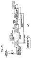
- FIG. 20 is a block diagram showing the structure of an optical receiving circuit 20 according to the third embodiment of the present invention.
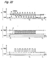
- FIGS. 21 to 23 each indicate a signal waveform in the main part of the optical receiving circuit 20.
- the optical receiving circuit 20 is placed in an optical transmission system of the burst-mode.
- the optical receiving circuit 20 is provided with a linear amplifying circuit 21, a comparing circuit 22, and a communication controller 23 as alternatives to the preamplifier 16, the linear amplifying circuit 17, the reference signal generator 18, and the comparator 19. There is no more difference therebetween, thus other components share the same reference numerals.
- an electrical-optical conversion device of a semiconductor laser is driven by electrical burst-mode data, and an optical burst-mode signal having such waveform as exemplarily shown in FIG. 21A is generated. More specifically, the burst-mode data is generated in the signal period T 2 in FIG. 21A, and only therein, the electrical-optical conversion device responds to the burst-mode data for light emission or extinction. The optical burst-mode signal is thus generated, and time intervals except the signal period T 2 become the non signal period T 1 .
- the optical burst-mode signal is a single-phase signal, which takes either a level equal to or higher than a reference value V 1 (base value) or a level equal to or lower.
- FIG. 21A exemplarily shows a single-phase signal varies only in the level equal to or higher than the reference level V 1 .
- the reference value V 1 is equal to "Low" for the single-phase signal.
- the optical/electrical conversion device 15 receives such optical burst-mode signal.
- the optical/electrical conversion device 15 subjects the received optical burst-mode signal to optical-electrical conversion, and generates an electrical burst-mode signal responding to light emission or extinction of the electrical-optical conversion for output to the signal period T 2 .
- the electrical burst-mode signal is also a single-phase signal as is the optical burst-mode signal, and is transmitted to the linear amplifying circuit 21. Contrarily, the optical/electrical conversion device 15 outputs no signal to the non signal period T 1 since the electrical-optical conversion device remains extinguished.
- the linear amplifying circuit 21 in FIG. 20 is preferably implemented as the one disclosed in United States Patent No. 5875049.
- the linear amplifying circuit 21 converts the single-phase signal provided by the optical/electrical conversion device 15 into a bi-phase signal.
- the bi-phase signal is then so amplified as to be in a constant amplitude level by automatic gain control (AGC) of the linear amplifying circuit 21.
- AGC automatic gain control
- the linear amplifying circuit 21 also generates a reference signal for use in the comparing circuit 22 subsequent thereto.
- a waveform ⁇ in FIG. 21B indicates the bi-phase signal generated in the linear amplifying circuit 21.
- the bi-phase signal varies in both levels (positive and negative) with reference to a reference value V 2 .
- the reference value V 2 indicates a level of the bi-phase signal in the non signal period T 1 .
- a waveform ⁇ in FIG. 21B indicates the reference signal generated by the linear-amplifying circuit 21.
- the reference signal is in a constant level, which is substantially equal to the reference value V 2 . In other words, the reference signal is set equal to an intermediate value of the amplification of the bi-phase signal.
- the waveform ⁇ of the bi-phase signal overlaps with the waveform ⁇ of the reference signal. Strictly, as indicated in a dot-lined ellipse in FIG. 21B, a thermal noise component occurred in the linear amplifying circuit 21 is superimposed on the bi-phase signal. The waveform ⁇ thereof thus fluctuates in the positive and negative directions with respect to the waveform ⁇ of the reference signal. Such bi-phase signal and the reference signal are both forwarded to the comparing circuit 22 as shown in FIG. 20.
- FIG. 24 is a block diagram showing the detailed structure of the comparing circuit 22.
- the comparing circuit 22 includes, as main components, a hysteresis controller 221, a comparator 222, and a differential amplifier 223.
- the hysteresis controller 221 includes an inverter 224, a first transistor 225, a second transistor 226, a first current source 227, a second current source 228, a first voltage-driven current source 229, and a second voltage-driven current source 2210.
- the structure of the comparing circuit 22 is described in detail next below.
- a gate of a third transistor 2212 is provided with the reference signal outputted from the linear amplifying circuit 21 through a signal line 2211.
- the third transistor 2212 is used as a source follower.
- the first current source 227 is coupled to a source of the third transistor 2212.
- one end of a signal line 2213 is connected between the source of the third transistor 2212 and the first current source 227.
- the other end thereof is coupled to a negative (-) input terminal of the comparator 222.
- a gate of a fourth transistor 2215 is provided with the bi-phase signal outputted from the linear amplifying circuit 21 through a signal 2214.
- the fourth transistor 2215 is used as a source follower.
- the second current source 228 is coupled to a source of the fourth transistor 2215.
- one end of a signal line 2216 is connected.
- the other end thereof is coupled to a positive (+) input terminal of the comparator 222.
- signal lines 2217 and 2218 are connected.
- the signal lines 2217 and 2218 are respectively connected to an input end of the differential amplifier 223.
- a signal line 2219 is connected.
- the signal lines 2217 and 2218 are both branched in partway.
- the branched signal lines 2217 and 2218 are coupled to the first and second voltage-driven current sources 229 and 2210.
- currents generated in the first and second current sources 227 and 228 are equal in value, and currents generated in the first and second voltage-driven current sources 229 and 2210 are also equal in value.
- a PREAMBLE-DETECTED signal similar to the one in the first embodiment is fed back from the digital PLL circuit 1. More specifically, the PREAMBLE-DETECTED signal is forwarded to the inverter 224 shown in FIG. 24.
- the inverter 224 inverts the received PREAMBLE-DETECTED signal therein.
- An output signal from the inverter 224 is a binary signal indicating both "High” and "Low” as shown in FIG. 21C.
- FIG. 21C shows a negative logic, and thus "High” indicates that the head of the burst-mode data is not yet detected, i.e., indicates the non signal period T 1 .
- the first and second transistors 225 and 226 are put ON when the output signal from the inverter 224 indicates "High", i.e., when the head of the burst-mode data is not yet detected (substantially non signal period T 1 ). Contrarily, when the output signal indicates "Low", i.e., when the head of the burst-mode data is already detected (substantially signal period T 2 ), the first and second transistors 225 and 226 are put OFF. In response thereto, the hysteresis controller 221 differently operates between the non signal period T 1 and the signal period T 2 . For convenience, It is first described how the comparing circuit 22 operates in the signal period T 2 , and then in the non signal period T 1 .
- the negative input terminal of the comparator 222 is provided with the value of the reference signal without any change.
- the bi-phase signal is provided as it is through the signal lines 2214 and 2216.
- the comparator 222 compares the value of the bi-phase signal provided to the positive input terminal with a constant threshold value (reference signal), and then outputs a positive-phase output (see waveform ⁇ in FIG. 22B) indicating the result to the signal line 2217. Further, the comparator 222 outputs a negative-phase (see waveform ⁇ in FIG. 22B) obtained by inverting the positive-phase to the signal line 2218.
- differential amplifier 223 recovers the electrical burst-mode data by converting the received differential signals into the single-phase signals.
- the burst-mode data recovered thereby is outputted to the subsequent digital PLL circuit 1 through the signal line 2219.
- the first and second transistors 225 and 226 are both put ON, and thus the hysteresis controller 221 operates.
- the positive-phase output indicates "High” and the negative-phase output "Low”.
- the positive-phase output indicating "High” is provided to the first voltage-driven current source 229 through the signal line 2217, whereby the electrical current passing therethrough is in a predetermined value.
- the second voltage-driven current source 2210 is provided with the negative-phase output indicating "Low” through the signal line 2218. The second voltage-driven current source 2210, however, does not operate thereby, therefore no current passes therethrough.
- the current generated in the first voltage-driven current source 229 passes through drain-source of the third transistor 2212. Accordingly, a voltage V 5 between an electrical potential of the signal line 2211 coupled to the gate of the third transistor 2212 and that of the signal line 2213 coupled to the source thereof becomes larger than the above-described voltage V 3 .
- a voltage V 6 between an electrical potential of the signal line 2214 coupled to the gate of the fourth transistor 2215 and that of the signal line 2216 coupled to the source thereof becomes equal to the above-described voltage V 4 . Therefore, the negative input terminal of the comparator 222 is lowered in input level compared with the positive input terminal thereof. In other words, the value of the reference signal becomes smaller than the reference value V 2 of the bi-phase signal.
- the second voltage-driven current source 2210 With the positive-phase output indicating "Low” and the negative-phase output "High", the second voltage-driven current source 2210 has an electrical current in a predetermined value passing therethrough but the first voltage-driven current source 229. The current generated in the second voltage-driven current source 2210 passes through drain-source of the fourth transistor 2215. Accordingly, a voltage V 7 between an electrical potential of the signal line 2214 coupled to the gate of the fourth transistor 2215 and that of the signal line 2216 coupled to the source thereof becomes larger than the above-described voltage V 4 .
- the negative input terminal of the comparator 222 becomes higher in an input level than the positive input terminal. In other words, the value of the reference signal becomes larger than the reference value V 2 of the bi-phase signal.
- the hysteresis controller 221 changes the value of the reference signal only in the non signal period T 1 .
- the comparing circuit 22 operates when received the reference signal and the bi-phase signal shown in FIG. 21B.
- the output signal from the inverter 224 shown in FIG. 21C indicates "High" (substantially without-signal T 1 )
- the reference signal provided to the signal line 2211 and the bi-phase signal provided to the signal line 2214 are substantially equal in value (see FIG. 21B).
- the offset value V OFFSET is preferably a value about double or three-times more than a dispersion value of the thermal noise component superimposed on the bi-phase signal in the linear amplifying circuit 21.
- the offset value V OFFSET as shown in FIG. 22A, the reference signal provided to the negative input terminal is set slightly higher in value than the bi-phase signal to the positive input terminal.
- the level of the bi-phase signal varies due to the thermal noise component superimposed in the linear amplifying circuit 21.
- the reference signal set preferably about double or three-times more than the distribution value of the thermal noise component, the level of the bi-phase signal hardly exceeds the value of the reference signal.
- the possibility for the comparator 222 to have a result indicating "High” is considerably reduced, and the non signal period T 1 never has an invariable value taking both "High” and "Low”.
- an output from the differential amplifier 223 is approximately constant in "Low”.
- the value of the reference signal provided to the signal line 2211 is equal to the reference value V 2 (average) of the bi-phase signal provided to the signal line 2214.
- the value of the reference signal provided to the negative input terminal remains in the value V 2 as shown in FIG. 22A.
- the comparator 222 compares an intermediate value of the bi-phase signal with the value of the bi-phase signal itself, thus the burst-mode data being the electrical signal outputted from the differential amplifier 223 hardly has pulse width distortion. Thus, the SN ratio of the burst-mode data is prevented from being lowered as is correctly discriminated at the center of the amplitude.
- the communication controller 23 shown in FIG. 20 is previously informed of an approximate time when the burst-mode data is over.
- the communication controller 23 When the time draws near, the communication controller 23 generates a reset signal.
- the reset signal is forwarded to the linear amplifying circuit 21 and the digital PLL circuit 1.
- a gain of the AGC amplifier is reset to the initial value.
- the digital PLL circuit 1 sets the PREAMBLE-DETECTED signal to "Low".
- PREAMBLE-DETECTED signal With such PREAMBLE-DETECTED signal, the output signal from the inverter 224 is changed to indicate "High", and thus the hysteresis controller 221 starts operation.
- the burst-mode data outputted from the comparing circuit 22 always indicates "Low".
- the comparing circuit 22 receives the bi-phase signal.
- the structure is only preferable but not restrictive, and thus the single-phase signal may be provided to the comparing circuit 22 without any change, although the bi-phase signal varying in level in positive and negative directions with respect to the reference value V 2 being more advantageous.
- the comparing circuit 22 can perform comparison processing with accuracy by using the reference signal having the reference value V2 set even if the amplitude level of the bi-phase signal is not sufficiently amplified in the linear amplifying circuit 21.
- the single-phase signal takes only either positive or negative with respect to the reference value V 1 . Therefore, if the amplitude level thereof is not sufficiently amplified, the comparing circuit 22 may not correctly perform the comparison processing.
- the comparing circuit 22 is set to receive the reference signal from the linear amplifying circuit 21, the comparing circuit 22 may be set to receive the reference signal from a reference power supply which is not shown.
- the digital PLL circuit 1 in FIG. 20 is described. Since the digital PLL circuit 1 in FIG. 20 is structurally and operationally similar to the one in the first embodiment, the description is made only to additional technical effects obtainable by the hysteresis controller 221.
- the hysteresis controller 221 controls the reference signal and thus the digital PLL circuit 1 hardly receives a signal invariable in value even in the non signal period T 1 .
- the digital PLL circuit 1 is assumed to receive randomly-generating data having "High” and "Low” in the non signal period T 1 . With this assumption, if the sampling circuit 3 samples such randomly-generating data utilizing the clock signals clk 1 to clk 8 as shown in FIGS. 2A and 2B, a signal to be outputted therefrom as 1 st to 8 th sampled burst mode data may have a 50/50 (0.5) possibility for "High” or "Low".
- these probability Pe 1 , Pe 2 , and Pe 3 each denote a probability for erroneously detecting, as the head of the burst-mode data, an incoming signal whose value is invariable.
- the probabilities Pe 1 , Pe 2 , and Pe 3 are regarded as being sufficiently small. Therefore, even if any bit error is caused in the digital PLL circuit 1 due to the erroneous detection of the head, there is no problem for practical use.
Landscapes
- Engineering & Computer Science (AREA)
- Computer Networks & Wireless Communication (AREA)
- Signal Processing (AREA)
- Synchronisation In Digital Transmission Systems (AREA)
- Optical Communication System (AREA)
Applications Claiming Priority (4)
| Application Number | Priority Date | Filing Date | Title |
|---|---|---|---|
| JP16870399 | 1999-06-15 | ||
| JP11168703A JP2000358021A (ja) | 1999-06-15 | 1999-06-15 | デジタルpll回路とそれを用いた光受信回路 |
| JP11223912A JP2001053734A (ja) | 1999-08-06 | 1999-08-06 | バースト光信号用の光受信回路 |
| JP22391299 | 1999-08-06 |
Publications (2)
| Publication Number | Publication Date |
|---|---|
| EP1061691A2 true EP1061691A2 (de) | 2000-12-20 |
| EP1061691A3 EP1061691A3 (de) | 2005-05-25 |
Family
ID=26492306
Family Applications (1)
| Application Number | Title | Priority Date | Filing Date |
|---|---|---|---|
| EP00111934A Withdrawn EP1061691A3 (de) | 1999-06-15 | 2000-06-15 | Digitale PLL-Schaltung für Burstbetrieb und optische Empfangsschaltung, die dieselbe verwendet |
Country Status (1)
| Country | Link |
|---|---|
| EP (1) | EP1061691A3 (de) |
Cited By (8)
| Publication number | Priority date | Publication date | Assignee | Title |
|---|---|---|---|---|
| WO2002078228A3 (en) * | 2001-03-27 | 2003-07-31 | Igor Anatolievich Abrosimov | Receiver with recovery circuit using oversampling and majority decision |
| EP1246388A3 (de) * | 2001-03-29 | 2006-06-07 | Fujitsu Limited | Taktrückgewinnungsschaltung und Empfangsschaltung |
| EP2061177A4 (de) * | 2006-09-04 | 2011-05-18 | Mitsubishi Electric Corp | Datenwiedergabeschaltung |
| EP2335374A4 (de) * | 2008-10-02 | 2012-03-28 | Zenko Technologies Inc | Datenabtastschaltung und verfahren zur takt- und datenwiedergewinnung |
| CN111817726A (zh) * | 2020-07-10 | 2020-10-23 | 上海兆芯集成电路有限公司 | 串行系统 |
| US11212072B1 (en) * | 2020-12-22 | 2021-12-28 | Xilinx, Inc. | Circuit for and method of processing a data stream |
| CN116052742A (zh) * | 2022-07-13 | 2023-05-02 | 成都海光集成电路设计有限公司 | 数据处理方法、装置、存储控制器、设备及介质 |
| WO2025190767A1 (en) | 2024-03-12 | 2025-09-18 | Universiteit Gent | Clock and data recovery circuitry for sampling a burst serial data signal |
Family Cites Families (2)
| Publication number | Priority date | Publication date | Assignee | Title |
|---|---|---|---|---|
| JP2773669B2 (ja) * | 1995-03-01 | 1998-07-09 | 日本電気株式会社 | ディジタルpll回路 |
| JP3072833B2 (ja) * | 1997-05-23 | 2000-08-07 | 日本電気株式会社 | ディジタルpll回路 |
-
2000
- 2000-06-15 EP EP00111934A patent/EP1061691A3/de not_active Withdrawn
Cited By (9)
| Publication number | Priority date | Publication date | Assignee | Title |
|---|---|---|---|---|
| WO2002078228A3 (en) * | 2001-03-27 | 2003-07-31 | Igor Anatolievich Abrosimov | Receiver with recovery circuit using oversampling and majority decision |
| EP1246388A3 (de) * | 2001-03-29 | 2006-06-07 | Fujitsu Limited | Taktrückgewinnungsschaltung und Empfangsschaltung |
| US7116744B2 (en) | 2001-03-29 | 2006-10-03 | Fujitsu Limited | Clock recovery circuit and receiver circuit for improving the error rate of signal reproduction |
| EP2061177A4 (de) * | 2006-09-04 | 2011-05-18 | Mitsubishi Electric Corp | Datenwiedergabeschaltung |
| EP2335374A4 (de) * | 2008-10-02 | 2012-03-28 | Zenko Technologies Inc | Datenabtastschaltung und verfahren zur takt- und datenwiedergewinnung |
| CN111817726A (zh) * | 2020-07-10 | 2020-10-23 | 上海兆芯集成电路有限公司 | 串行系统 |
| US11212072B1 (en) * | 2020-12-22 | 2021-12-28 | Xilinx, Inc. | Circuit for and method of processing a data stream |
| CN116052742A (zh) * | 2022-07-13 | 2023-05-02 | 成都海光集成电路设计有限公司 | 数据处理方法、装置、存储控制器、设备及介质 |
| WO2025190767A1 (en) | 2024-03-12 | 2025-09-18 | Universiteit Gent | Clock and data recovery circuitry for sampling a burst serial data signal |
Also Published As
| Publication number | Publication date |
|---|---|
| EP1061691A3 (de) | 2005-05-25 |
Similar Documents
| Publication | Publication Date | Title |
|---|---|---|
| US11063741B2 (en) | Phase control block for managing multiple clock domains in systems with frequency offsets | |
| US7099400B2 (en) | Multi-level pulse amplitude modulation receiver | |
| US7471755B2 (en) | Methods and arrangements for link power reduction | |
| EP0766393B1 (de) | Pulspositionsdemodulator | |
| US8054926B2 (en) | Clock and data recovery system and method for clock and data recovery based on a forward error correction | |
| US6850580B1 (en) | Bit synchronizing circuit | |
| JPWO2008126429A1 (ja) | クロック・データ再生回路およびその制御方法 | |
| US6389090B2 (en) | Digital clock/data signal recovery method and apparatus | |
| EP1061691A2 (de) | Digitale PLL-Schaltung für Burstbetrieb und optische Empfangsschaltung, die dieselbe verwendet | |
| US20030061564A1 (en) | Serial data extraction using two cycles of edge information | |
| US20030030576A1 (en) | Deserializer | |
| US7113560B1 (en) | Serial link scheme based on delay lock loop | |
| US4423518A (en) | Timing recovery circuit | |
| US7532695B2 (en) | Clock signal extraction device and method for extracting a clock signal from data signal | |
| US20050084048A1 (en) | Clock and data recovery circuit | |
| US7317777B2 (en) | Digital adaptive control loop for data deserialization | |
| US7466765B2 (en) | Receiver for high bitrate binary signals | |
| KR20030075140A (ko) | 데이터의 위치 정보 탐색을 통한 데이터 복원 방법 및상기 알고리즘을 적용한 직렬 데이터 수신기 | |
| KR100300947B1 (ko) | 디지털텔레비젼수신장치의세그먼트동기신호검출장치 | |
| US7729453B1 (en) | System and method for fast dynamic adjustment of slicing level for burst mode optical receivers | |
| US7136447B2 (en) | Clock recovery circuit | |
| KR19980083160A (ko) | 위상 보정 회로 및 그 방법 | |
| JPH104436A (ja) | クロック再生回路 | |
| US7006585B2 (en) | Recovering data encoded in serial communication channels | |
| JP2001053734A (ja) | バースト光信号用の光受信回路 |
Legal Events
| Date | Code | Title | Description |
|---|---|---|---|
| PUAI | Public reference made under article 153(3) epc to a published international application that has entered the european phase |
Free format text: ORIGINAL CODE: 0009012 |
|
| AK | Designated contracting states |
Kind code of ref document: A2 Designated state(s): AT BE CH CY DE DK ES FI FR GB GR IE IT LI LU MC NL PT SE |
|
| AX | Request for extension of the european patent |
Free format text: AL;LT;LV;MK;RO;SI |
|
| PUAL | Search report despatched |
Free format text: ORIGINAL CODE: 0009013 |
|
| AK | Designated contracting states |
Kind code of ref document: A3 Designated state(s): AT BE CH CY DE DK ES FI FR GB GR IE IT LI LU MC NL PT SE |
|
| AX | Request for extension of the european patent |
Extension state: AL LT LV MK RO SI |
|
| AKX | Designation fees paid | ||
| STAA | Information on the status of an ep patent application or granted ep patent |
Free format text: STATUS: THE APPLICATION IS DEEMED TO BE WITHDRAWN |
|
| 18D | Application deemed to be withdrawn |
Effective date: 20060223 |
|
| REG | Reference to a national code |
Ref country code: DE Ref legal event code: 8566 |