EP1061732A1 - Verfahren zur durch ihre zugehörigen Dioden/Photodioden Polarisierung der Photodioden eines Matrixsensors - Google Patents
Verfahren zur durch ihre zugehörigen Dioden/Photodioden Polarisierung der Photodioden eines Matrixsensors Download PDFInfo
- Publication number
- EP1061732A1 EP1061732A1 EP00401656A EP00401656A EP1061732A1 EP 1061732 A1 EP1061732 A1 EP 1061732A1 EP 00401656 A EP00401656 A EP 00401656A EP 00401656 A EP00401656 A EP 00401656A EP 1061732 A1 EP1061732 A1 EP 1061732A1
- Authority
- EP
- European Patent Office
- Prior art keywords
- photodiodes
- photodiode
- diodes
- voltage
- circuit
- Prior art date
- Legal status (The legal status is an assumption and is not a legal conclusion. Google has not performed a legal analysis and makes no representation as to the accuracy of the status listed.)
- Withdrawn
Links
- 238000000034 method Methods 0.000 title claims description 22
- 239000011159 matrix material Substances 0.000 title description 9
- 238000001514 detection method Methods 0.000 claims abstract description 96
- 239000000758 substrate Substances 0.000 claims description 41
- 102100030762 Apolipoprotein L1 Human genes 0.000 claims description 11
- 101100237637 Bos taurus APOL gene Proteins 0.000 claims description 11
- 101100323521 Homo sapiens APOL1 gene Proteins 0.000 claims description 11
- 230000010287 polarization Effects 0.000 abstract description 17
- 238000010586 diagram Methods 0.000 description 22
- 239000000463 material Substances 0.000 description 20
- 238000004519 manufacturing process Methods 0.000 description 19
- 238000005286 illumination Methods 0.000 description 12
- 239000004065 semiconductor Substances 0.000 description 12
- 230000008569 process Effects 0.000 description 9
- 230000004044 response Effects 0.000 description 8
- 239000010410 layer Substances 0.000 description 7
- 238000006243 chemical reaction Methods 0.000 description 6
- 238000002513 implantation Methods 0.000 description 5
- 239000007787 solid Substances 0.000 description 5
- 230000003595 spectral effect Effects 0.000 description 5
- 230000000694 effects Effects 0.000 description 4
- 239000012212 insulator Substances 0.000 description 4
- 239000011325 microbead Substances 0.000 description 4
- 210000004027 cell Anatomy 0.000 description 3
- 239000007943 implant Substances 0.000 description 3
- 230000005855 radiation Effects 0.000 description 3
- 230000009467 reduction Effects 0.000 description 3
- 238000012163 sequencing technique Methods 0.000 description 3
- 229910000661 Mercury cadmium telluride Inorganic materials 0.000 description 2
- 230000000712 assembly Effects 0.000 description 2
- 238000000429 assembly Methods 0.000 description 2
- 230000003416 augmentation Effects 0.000 description 2
- 230000005540 biological transmission Effects 0.000 description 2
- 238000005516 engineering process Methods 0.000 description 2
- 230000004313 glare Effects 0.000 description 2
- 229910052738 indium Inorganic materials 0.000 description 2
- APFVFJFRJDLVQX-UHFFFAOYSA-N indium atom Chemical compound [In] APFVFJFRJDLVQX-UHFFFAOYSA-N 0.000 description 2
- 238000012545 processing Methods 0.000 description 2
- 238000012552 review Methods 0.000 description 2
- UFYXKDMLGBKHIC-UHFFFAOYSA-N 3-(4-hydroxy-2-phenylphenanthren-3-yl)-2-phenylphenanthren-4-ol Chemical compound C=1C2=CC=C3C=CC=CC3=C2C(O)=C(C=2C(=CC3=C(C4=CC=CC=C4C=C3)C=2O)C=2C=CC=CC=2)C=1C1=CC=CC=C1 UFYXKDMLGBKHIC-UHFFFAOYSA-N 0.000 description 1
- 229910004613 CdTe Inorganic materials 0.000 description 1
- 229910004611 CdZnTe Inorganic materials 0.000 description 1
- XUIMIQQOPSSXEZ-UHFFFAOYSA-N Silicon Chemical compound [Si] XUIMIQQOPSSXEZ-UHFFFAOYSA-N 0.000 description 1
- 238000013459 approach Methods 0.000 description 1
- 239000003990 capacitor Substances 0.000 description 1
- 230000015556 catabolic process Effects 0.000 description 1
- 230000001143 conditioned effect Effects 0.000 description 1
- 238000005520 cutting process Methods 0.000 description 1
- 230000007123 defense Effects 0.000 description 1
- 238000006731 degradation reaction Methods 0.000 description 1
- 238000013461 design Methods 0.000 description 1
- 238000011161 development Methods 0.000 description 1
- 238000009826 distribution Methods 0.000 description 1
- 230000009977 dual effect Effects 0.000 description 1
- 235000021183 entrée Nutrition 0.000 description 1
- 238000000407 epitaxy Methods 0.000 description 1
- 230000004907 flux Effects 0.000 description 1
- 238000005304 joining Methods 0.000 description 1
- 230000028161 membrane depolarization Effects 0.000 description 1
- 239000000615 nonconductor Substances 0.000 description 1
- 230000003287 optical effect Effects 0.000 description 1
- 230000002093 peripheral effect Effects 0.000 description 1
- 238000007789 sealing Methods 0.000 description 1
- 229910052710 silicon Inorganic materials 0.000 description 1
- 239000010703 silicon Substances 0.000 description 1
- 239000002356 single layer Substances 0.000 description 1
- 230000035882 stress Effects 0.000 description 1
- 230000008646 thermal stress Effects 0.000 description 1
- 238000001931 thermography Methods 0.000 description 1
- 238000011144 upstream manufacturing Methods 0.000 description 1
- 238000010200 validation analysis Methods 0.000 description 1
Images







Classifications
-
- H—ELECTRICITY
- H04—ELECTRIC COMMUNICATION TECHNIQUE
- H04N—PICTORIAL COMMUNICATION, e.g. TELEVISION
- H04N25/00—Circuitry of solid-state image sensors [SSIS]; Control thereof
- H04N25/70—SSIS architectures; Circuits associated therewith
- H04N25/76—Addressed sensors, e.g. MOS or CMOS sensors
- H04N25/766—Addressed sensors, e.g. MOS or CMOS sensors comprising control or output lines used for a plurality of functions, e.g. for pixel output, driving, reset or power
-
- H—ELECTRICITY
- H04—ELECTRIC COMMUNICATION TECHNIQUE
- H04N—PICTORIAL COMMUNICATION, e.g. TELEVISION
- H04N23/00—Cameras or camera modules comprising electronic image sensors; Control thereof
- H04N23/20—Cameras or camera modules comprising electronic image sensors; Control thereof for generating image signals from infrared radiation only
-
- H—ELECTRICITY
- H04—ELECTRIC COMMUNICATION TECHNIQUE
- H04N—PICTORIAL COMMUNICATION, e.g. TELEVISION
- H04N25/00—Circuitry of solid-state image sensors [SSIS]; Control thereof
- H04N25/60—Noise processing, e.g. detecting, correcting, reducing or removing noise
- H04N25/67—Noise processing, e.g. detecting, correcting, reducing or removing noise applied to fixed-pattern noise, e.g. non-uniformity of response
- H04N25/671—Noise processing, e.g. detecting, correcting, reducing or removing noise applied to fixed-pattern noise, e.g. non-uniformity of response for non-uniformity detection or correction
- H04N25/677—Noise processing, e.g. detecting, correcting, reducing or removing noise applied to fixed-pattern noise, e.g. non-uniformity of response for non-uniformity detection or correction for reducing the column or line fixed pattern noise
Definitions
- the invention lies in the field of radiation detector networks electromagnetic, in particular radiation visible or infrared.
- the domain is more limited particularly to image sensors (ref. [1], [2] in the list appearing in appendix) made up of a circuit of detection interconnected to a read circuit. She relates to a device and a method for polarizing such photodetectors.
- a photodiode is a device semiconductor which when illuminated by a sufficient energy radiation, delivers a photocurrent by generation of electron-hole pairs.
- Two categories of photodiodes can be produced, depending on the type of doping of the junctions and the substrate, the N-type junction on semiconductor material type P and its dual, junction P on material N.
- the detection circuit is generally formed of an arrangement of implanted elementary photodiodes at a regular step according to a matrix of m lines by n columns where all the junctions are coplanar.
- Each photodiode is coupled to a preamplifier installed on the reading circuit which ensures the conversion of the photocurrent delivered by the detector into a physical quantity compatible with the chains of analog processing achievable in circuits integrated (current, load or voltage).
- the functions installed on the reading circuit also allow to multiplex the information delivered by each photodiode to a limited number of video outputs.
- the information delivered by each photodiode and conditioned by the analog chain of the circuit read corresponds to an element of the image or pixel.
- Detection circuit can be illuminated either on the face where the junctions are made, or on the opposite side.
- the detection circuit is interconnected to the reading circuit by means of a suitable process, for example microbeads in the case sensors produced by means of a hybrid detection returned on a read circuit (ref. [3]).
- the principle of photovoltaic detection allows, for example, to realize image sensors operating in the spectral band of the visible domain, or in that of infrared (thermal imaging).
- the spectral band selectivity is obtained by performing photodiodes junctions on a material semiconductor whose band width is prohibited is adapted to the wavelength to be detected.
- the invention relates to the method used to polarize the photodiodes of the detection circuit.
- the review of the state of the art will hereinafter focus on the problem of the polarization of photodiodes of these sensors.
- the operating principle of the sensor will be first recalled, then the impact of the material on which is carried out the detection circuit on the controllability - that is, the ability to force a level, in this case to apply a source of voltage - electrical nodes of photodiodes.
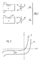
- Figure la represents on the one hand, a cross across the thickness of a junction between a substrate 1 P-doped semiconductor and an N-doped zone 2 performing a N / P junction.
- the representation symbolic is constituted by the representation symbolic of a diode 3 whose anode 4 is located above cathode 5, so as to show that it is the substrate which is doped P.
- FIG. 1b represents the same elements, but this time it is the substrate 1 which is doped N.
- a zone 2 'doped P is implanted on this substrate 1' performing a P / N junction. Symbolically, this junction is represented by a 3 'diode whose anode 4 'is located below the cathode 5' so that show that it is the substrate 1 'which is doped N.
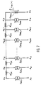
- the current-voltage characteristic of such a junction is represented in FIG. 2.
- curve (a) we find the non-linear characteristic of the ideal junction under zero illumination: low dynamic impedance when the diode is polarized in direct, the voltage of the anode being greater than the cathode voltage, and on the contrary high dynamic impedance when the photodiode is reverse biased with an anode voltage lower than the cathode voltage.
- the current-voltage characteristic, represented by the curve (b) is translated vertically by an amount I P equal to the photocurrent generated by the photodiode.
- I P the current-voltage characteristics of photodiodes are represented in conventional quadrants and not with the actual signs of currents and voltages.
- FIG. 3 The block diagram of a sensor is shown in Figure 3, it corresponds to the section of a matrix sensor, perpendicular to the planes of layers, in one of the directions of the lines or columns of the detector array.
- This diagram illustrates the case of a hybridized detection circuit 17, returned to a read circuit 20 as mentioned, for example, in document [2].
- the N photodiodes of the row corresponding to the section plane are marked from D 1 to D N , their anodes from A 1 to A N and their cathodes from K 1 to K N.
- the anodes of the photodiodes of the detection circuit 17 are connected to the inputs E 1 ?? E N of the reading circuit 20.
- the continuity between the detection 17 and reading 20 circuits is ensured by a vertical connection, for example of the type indium microbead 21.
- the preamplifiers of the read circuit 20 are numbered from PA 1 to PA N.
- the process is repeated at the frequency of the image.
- each photodiode is polarized in the reverse part of its characteristic, to a voltage where the intensity of its current under illumination none is relatively small compared to the intensity of its photocurrent. Controlling the difference in potential between the anode and the cathode of each photodiode is therefore decisive in the operation of the detection circuit.
- each anode is controlled by the input of the preamplifier (virtual ground of a differential amplifier for example).
- the cathodes of each photodiode are not individually controllable. They are in fact short-circuited by the semiconductor material where the junctions are made. The cathodes K 1 to K N can therefore only be controlled indirectly, via a single electrical node of the detection circuit identified K C - for common cathode.
- the solid substrate, figure 4-A consists of a single layer 6 over the entire thickness of the wafer.
- the resistivity ⁇ 1 of the layer is homogeneous and suitable for producing efficient junctions from a photodetection point of view.
- the epitaxial substrate, figure 4-B, is a bi-layer 7, 8.
- the junctions of the photodiodes are carried out in the upper layer 7 of thin thickness and of resistivity ⁇ 2 suitable for the realization of the photodiodes.
- the lower layer 8 is made of the same material. It is very thick and its resistivity ⁇ 3 is very low, so as to minimize the resistance to access to the cathodes of the junctions.
- the detection circuits operating in the spectral range of the visible are made on solid or epitaxial silicon substrates, or even insulator (ref. [1]). Those operating in the range infrared spectral are rather realized on insulating substrates (e.g. material HgCdTe semiconductor on CdZnTe insulator of ref. [2]). In all cases, the photodiodes are coplanar.
- the common cathode of the photodiodes of detection circuits 17 made on the substrates massive or epitaxial can obviously be controlled ensuring electrical continuity between a source tension 11 and a contact 12 made on the face opposite 13 to the junctions 1,2 of the detection circuit.
- This solution shown in Figure 5, is however not always applicable.
- the technological manufacturing process must integrate additional steps in order to achieve the ohmic contact 12 on the face 13 opposite the junctions 1,2. Then, for the sensors lit through the face 13 of the substrate, the loss of light flux at the ohmic contact 12 of the face 13 of the substrate, or even its attenuation throughout the crossing may prove to be unacceptable.
- the manufacturing process of the detection in this case incorporates technological steps which make it possible, in addition to the junctions 1,2 of type N on type P semiconductor material, a ohmic contact 12 on this material.
- FIG. 6 A principle section of such a detection circuit 17 is shown in FIG. 6.
- the N + 2 zones materialize the anodes of the photodiodes.
- the P ++ zone materializes the ohmic contact 12 on the P type material.
- this method releases the face 13 opposite the junctions of any electrical stress linked to the common cathode. It is thus possible to optimize the optical response circuits lit through their substrate, by example by removing all or part of the sole of the substrate.
- contact ohmic 12 of the common cathode is implanted at the periphery of the area occupied by the photodiodes.
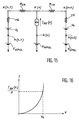
- Each photodiode behaves like a generator of a current IA K1 .... IA KN .
- the current generated for each photodiode crosses the resistors R IK separating the photodiode from the resistor R AKC and the resistor R AKC itself so that the latter is crossed by the sum of the currents of the photodiodes.
- This one-dimensional diagram is sufficient for the demonstration. Its generalization to a two-dimensional detection circuit leads to a two-dimensional network of intercathode electrical resistors, each photodiode being connected with the photodiodes implanted on its four sides and to resistors for access to the common cathode which vary according to the distribution of the P ++ zones on the periphery of the photodiodes on one side, two adjacent sides, two parallel sides or even on the four sides of the photodiodes array.
- This matrix 16 comprises a set of junctions 1, 2, arranged in a matrix.
- a P ++ 12 contact constituting a closed line surrounds the matrix assembly 16 of junctions 1,2.
- the limits 30 of the detection circuit 17 are represented by a closed dotted line 30.
- each photodiode D n can be assimilated as explained above in connection with FIG. 7 to a current generator of value I AKN .
- I AKN a current generator of value
- the electric diagram of FIG. 9 clearly shows that the currents delivered by the photodiodes are summed as one approaches the electric node K C.
- the circulation of these currents in the resistors R IK causes a fall in potential which is all the greater as the distance from the node K C increases .
- the potential of each cathode K N is therefore not equal to the voltage applied to the common cathode node K C.
- This polarization technique introduces a spatial variation of the voltage applied to the cathode photodiodes: photodiodes are not, everything being equal otherwise, polarized under the same potential difference between anode and cathode.
- the spatial variation of the point of operation of photodiodes has the effect, from a certain threshold to reduce the performance of the sensor because the optimal polarization range is seen scaled down.
- the amplitude of the spatial variation of the depolarization is all the more important as the number of sides on which the 12 P ++ ohmic contact can be implanted is reduced.
- the answer to a limited over-illumination in space is a determining criterion in a sensor image.
- the response of the photodiodes of the overlit area must not modify the response of photodiodes located outside this area.
- the electro-optical response over-lit photodiodes introduces a variation of the electro-optical response of all or part of the other photodiodes of the detection circuit while their illumination has not varied. This phenomenon can by example cause false alarms.
- the P ++ 12 contact of the common cathode is generally as shown in FIG. 8 located at the periphery of the detection circuit.
- the overall dimensions of the detection circuit 17 are significantly increased compared to the dimensions of the sensitive area 16 occupied by the array of photodiodes.
- This method therefore does not make it possible to maximize the filling rate of the detection circuit 17 by its photodiodes, which results in a loss of material at given number of pixels, or else a reduction of the number of pixels to circuit dimensions 17 data detection.
- the technological processes used to produce the ohmic contacts and the interconnections must be compatible with both the P ++ zones and the N + zones.
- the choice of technological processes is therefore more limited than in the case where it is only necessary to ensure electrical continuity with the N + zones.
- the invention eliminates the need for keep the ohmic contact 12. In this way we can obtain a set of coplanar photodetectors constituting together an image detection circuit, each photodetector generally constituting a pixel of the image, in which the value of the signal delivered by one of the photodetectors is not modified or is little modified by the value of the signal delivered by others sensor photodetectors. It aims to obtain a detection circuit with greater surface density, that is to say having a greater number of photodetectors per unit area of a circuit detection. Finally, it aims to simplify the manufacture of a detection circuit.
- the voltage V apol which is applied to the anodes of the photodiodes or detection diodes to polarize them is the detection voltage.
- the voltage V kpol which is applied to the anodes of the diodes of the second set or control diodes to polarize them is the control voltage.
- the control voltage applied to an anode of a control diode imposes a potential on the cathode of the neighboring diodes.
- the influence of a glare of a diode or group of diodes neighboring detectors of each other is limited to part of the detector delimited by a line joining the points of application of the voltage of reference which are closest to the junctions located at the limit of the dazzled part of the detector.
- the application of the reference voltage can be carried out by conductive bushings of the read circuit, applied directly to the detection circuit via junctions of the live polarized detection circuit so as to obtain low junction impedances.
- These diodes can be diodes dedicated only to the polarization.
- the invention also relates to a method of polarizing the photodiodes of a circuit detection of an image sensor, the detection circuit having on the same substrate, two coplanar assemblies of diodes, a first comprising photodiodes coplanar and a second with diodes coplanar control, each diode of each of assemblies having an anode and a cathode, and a diode control being connected to at least one photodiode, process characterized in that one applies to the anodes of the diodes of the first set a polarizing voltage in reverse the diodes of the first set and in that we apply diodes from the second set to the anodes a voltage direct polarizing said diodes of the second set.
- FIGS 1, 2, 3, 4 are figures that apply equally to art prior to the present invention.
- FIGS 5, 6, 7, 8, 9 are figures that illustrate or explain aspects of art prior.
- FIGS. 10 to 20 illustrate aspects and explanations relating to the present invention.
- the invention consists in imposing, by controlling the anode voltage of control diodes, the cathode voltage of each photodiode so as to equalize the apparent impedances of each photodiode.
- FIGS. 10 and 11 Geometric modes of implantation of such diodes are shown in FIGS. 10 and 11.
- Figure 10 shows the case of a bar linear photodetector where all the space necessary to implant control diodes is available.
- control diodes 18 can be aligned on a line parallel to the photodiodes implantation line 19. In the example shown in Figure 10 each control diode 18 is found to the right of a photodiode 19.
- control diodes 18 In the case of a represented matrix schematically figure 11, the place taken by the control diodes is necessarily at the expense of the surface density of photodiodes. It is why in this implantation mode we would be interested in give the control diodes 18 a form based on narrow lines; for example at an angle. It's such exemplary embodiment which is represented in FIG. 11 or each photodiode 19 of square shape is surrounded on two sides of the diode by the two branches of the square formed by the control diode 18.
- control diode can be a photodiode polarized live so as to have a low dynamic resistance, or a dedicated diode.
- control diodes and the photodiodes are all photodiodes. These photodiodes will be reverse biased alternately or live to operate as a photodiode or as control diode.
- the photodiodes 19 are materialized by N + junctions on a P type semiconductor material 1 and of resistivity p SC .
- the substrate can be solid, epitaxial or insulating and all the photodiodes are coplanar.
- This ohmic contact 12 is no longer necessary for the cathode voltage since according to the preferred embodiment, this cathode voltage is controlled by photodiodes of the circuit live polarized detection.
- the preferred embodiment of the invention may be produced on a substrate comprising an ohmic contact 12, this contact serving no purpose other than respecting a manufacturing protocol before validation of a new one protocol or having another use.
- the electrical diagram of the row of photodiodes in Figure 12 is shown in Figure 13 where the resistance R IK represents the resistance between two connected cathodes. Its value depends on the resistivity ⁇ SC and the thickness of the semiconductor material, the pitch of the photodiodes and the geometric characteristics of the junction (surface, depth).
- the cathode of photodiodes 3, shown in FIG. 13, is controllable by the read circuit.
- a voltage source V APOL is applied to the anode A [n] of the photodiode D [n], and the voltage source V KPOL to the anode of the connected photodiodes, in this case in this one-dimensional example, the photodiodes D [n-1] and D [n + 1].
- V K [n] V KPOL + V o
- each reverse polarized photodiode is surrounded by two direct polarized photodiodes, the current delivered by the reverse polarized photodiode is therefore distributed by fractions assumed to be equal in each of polarization diodes.
- the number of related photodiodes used to polarize the cathode of a detection photodiode can be optimized depending on the application envisaged (number of pixels, image format, resistivity of the semiconductor material, dynamic lighting).
- the configuration shown in part A with a line of control diodes connected to a line of photodetection diodes can be the same for all detector photodiodes except for one line located at the edge of the detector. This last possibility depends on the parity of the number of lines, even or odd number of lines and how line diodes are used alternately as control diodes.
- a line of polarized photodiodes in opposite is bordered on both sides by a line of diodes polarized in direct and ensuring a function of cathode voltage transmission it is clear that the photodiodes lines located on the edge cannot be polarized in the same way as photodiodes central lines.
- Non-uniformity of response of photodiodes installed on the periphery of a circuit two-dimensional detection can be offset by implantation of control photodiodes so that that the boundary conditions are identical for the periphery detection photodiodes and those located at the heart of the detection circuit.
- This example shows that the invention makes it possible to polarize the photodiodes of a detection circuit two-dimensional alternately using each photodiode as a detection device and then as control device for its photodiode (s) related.
- Polarization sequencing for the shooting of a complete image corresponds to the case shown in figure 17 part B, where the photodiodes of the even rows or columns are used alternately as photodiodes or as control diodes. Multiplexing of information then makes it possible to reconstruct the image complete.
- photodiodes which are alternately used as photodiodes or diodes control are the diodes located on the boxes white of a checkerboard and those located on the boxes black as shown in figure 17 part C, an image complete consists of half of the photodiodes available.
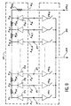
- Figure 19 shows an electrical diagram in principle of a matrix sensor operating in the infrared spectral range.
- the photodiodes 3 of the detection circuit are N + junctions produced on an epitaxy of P-type HgCdTe on an insulating substrate in CdTe.
- the anodes 4 of the photodiodes 3 of the detection circuit 17 are interconnected by microbeads 21 to the analog circuitry located on the reading circuit 20 under each photodiode.
- Each of these photodiodes 3 constitutes an elementary point of the detection circuit 17 of the sensor. It corresponds to it in a one-to-one way an elementary point of the reading circuit PEL constituted by a charge preamplifier 23.
- the charge preamplifier 23 constituting each PEL 23 ensures in known manner the conversion of the current delivered by each photodiode 3 in a voltage which will be multiplexed to a video output 24.
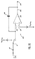
- the basic electrical diagram of the electronics implanted in the PEL 23 is given in FIG. 20.
- the charge amplifier 23 is produced by means of a voltage amplifier 25 with differential inputs 26, 27.
- a capacitor 28 is implanted in feedback between its output 29 and its inverting input 26.
- Its differential input 27 is a virtual ground: the input voltage of its inverting input 26 is equal to the voltage applied to its non-inverting input 27.
- the voltage source V APOL corresponding to the reverse bias of the diode is applied in a known manner to the non-inverting input 27.
- This sensor operates according to the sequencing described in connection with FIG. 18.
- the shooting of the even columns (resp. Odd) is carried out by closing the switches S of the odd columns (resp. Even ) on V KPOL while the switches S of even columns (resp. odd) are closed on the inverting inputs 26 of the amplifier 25.
- the information is memorized by opening the switch S of the even columns (resp. odd).
- each ELP 23 Information stored in each ELP 23 are multiplexed in a known manner to output 24 when shooting even columns and those odd columns are completed. We thus obtain all the pixels of a frame of the image.
- each photodiode of detection closes on a power supply through the related photodiodes polarized live.
- the potential difference across each photodiode detection is independent of its position on the detection circuit.
- the invention therefore makes it possible to polarize the cathode of each photodiode without spatial variations.
- the currents delivered by the detection photodiodes over-lit closes via their related LEDs control.
- the cathode voltage of the photodiodes of detection outside the over-lit area is therefore not disturbed by the circulation of photocurrents induced by over-illumination.
- the invention therefore limits the effects electrics induced by local over-illumination at the over-lit area.
- the invention makes it possible to implant photodiodes on the entire detection circuit, to the edge of the cutting path.
- the invention uses identical junctions as a photodetection and / or control device.
- the rules for drawing these junctions make it possible to install them at a minimum spacing which generally turns out to be much less than that between an N + junction and an ohmic contact on P type material.
- the invention therefore makes it possible to minimize the overall dimensions of the detection circuit.
- the invention makes it possible to polarize the cathodes photodiodes without using an ohmic contact on material P. Technological stages necessary for its realization can therefore be deleted.
- the invention makes it possible to manufacture circuits detection using only technological steps necessary for the realization of the photodiodes.
- Reducing the number of stages of manufacturing has the effect of increasing the yield of manufacturing, reduce manufacturing time.
Landscapes
- Engineering & Computer Science (AREA)
- Multimedia (AREA)
- Signal Processing (AREA)
- Transforming Light Signals Into Electric Signals (AREA)
- Solid State Image Pick-Up Elements (AREA)
Applications Claiming Priority (2)
| Application Number | Priority Date | Filing Date | Title |
|---|---|---|---|
| FR9907540A FR2795271B1 (fr) | 1999-06-15 | 1999-06-15 | Procede de polarisation des photodiodes d'un capteur matriciel par leurs pixels connexes |
| FR9907540 | 1999-06-15 |
Publications (1)
| Publication Number | Publication Date |
|---|---|
| EP1061732A1 true EP1061732A1 (de) | 2000-12-20 |
Family
ID=9546791
Family Applications (1)
| Application Number | Title | Priority Date | Filing Date |
|---|---|---|---|
| EP00401656A Withdrawn EP1061732A1 (de) | 1999-06-15 | 2000-06-13 | Verfahren zur durch ihre zugehörigen Dioden/Photodioden Polarisierung der Photodioden eines Matrixsensors |
Country Status (3)
| Country | Link |
|---|---|
| US (1) | US6707497B1 (de) |
| EP (1) | EP1061732A1 (de) |
| FR (1) | FR2795271B1 (de) |
Cited By (1)
| Publication number | Priority date | Publication date | Assignee | Title |
|---|---|---|---|---|
| EP2043362B1 (de) * | 2007-09-27 | 2016-12-28 | Commissariat à l'Énergie Atomique et aux Énergies Alternatives | Pixelmatrix, die mit Spannungsreglern ausgestattet ist |
Families Citing this family (5)
| Publication number | Priority date | Publication date | Assignee | Title |
|---|---|---|---|---|
| AT414053B (de) * | 2003-10-08 | 2006-08-15 | Efkon Ag | Infrarot (ir)-empfangseinrichtung |
| WO2007063893A1 (ja) * | 2005-11-29 | 2007-06-07 | Kabushiki Kaisha Topcon | レベルセンサ |
| CN103109525B (zh) * | 2008-10-08 | 2016-04-06 | 法国原子能委员会 | 一种矩阵微电子装置 |
| JP5272686B2 (ja) * | 2008-11-28 | 2013-08-28 | 富士通株式会社 | 光受信器、光受信回路および光受信方法 |
| US10644044B2 (en) | 2018-05-31 | 2020-05-05 | National Research Council Of Canada | Methods of manufacturing printable photodetector array panels |
Citations (3)
| Publication number | Priority date | Publication date | Assignee | Title |
|---|---|---|---|---|
| JPS6269671A (ja) * | 1985-09-24 | 1987-03-30 | Matsushita Electronics Corp | イメ−ジセンサ |
| US5168338A (en) * | 1991-09-30 | 1992-12-01 | Mitsubishi Denki Kabushiki Kaisha | Solid-state hybrid infrared imaging device |
| EP0670656A2 (de) * | 1994-03-03 | 1995-09-06 | Philips Electronics Uk Limited | Bildaufnahmevorrichtung |
Family Cites Families (3)
| Publication number | Priority date | Publication date | Assignee | Title |
|---|---|---|---|---|
| US4764682A (en) * | 1986-09-16 | 1988-08-16 | Ovonic Imaging Systems, Inc. | Photosensitive pixel sized and shaped to optimize packing density and eliminate optical cross-talk |
| JP2686036B2 (ja) * | 1993-07-09 | 1997-12-08 | 浜松ホトニクス株式会社 | アバランシェフォトダイオードのバイアス回路 |
| FR2736782B1 (fr) | 1995-04-07 | 1997-11-14 | Commissariat Energie Atomique | Dispositif et procede de lecture d'une matrice de detecteurs photoniques |
-
1999
- 1999-06-15 FR FR9907540A patent/FR2795271B1/fr not_active Expired - Fee Related
-
2000
- 2000-06-01 US US09/584,848 patent/US6707497B1/en not_active Expired - Fee Related
- 2000-06-13 EP EP00401656A patent/EP1061732A1/de not_active Withdrawn
Patent Citations (3)
| Publication number | Priority date | Publication date | Assignee | Title |
|---|---|---|---|---|
| JPS6269671A (ja) * | 1985-09-24 | 1987-03-30 | Matsushita Electronics Corp | イメ−ジセンサ |
| US5168338A (en) * | 1991-09-30 | 1992-12-01 | Mitsubishi Denki Kabushiki Kaisha | Solid-state hybrid infrared imaging device |
| EP0670656A2 (de) * | 1994-03-03 | 1995-09-06 | Philips Electronics Uk Limited | Bildaufnahmevorrichtung |
Non-Patent Citations (1)
| Title |
|---|
| PATENT ABSTRACTS OF JAPAN vol. 011, no. 265 (E - 535) 27 August 1987 (1987-08-27) * |
Cited By (1)
| Publication number | Priority date | Publication date | Assignee | Title |
|---|---|---|---|---|
| EP2043362B1 (de) * | 2007-09-27 | 2016-12-28 | Commissariat à l'Énergie Atomique et aux Énergies Alternatives | Pixelmatrix, die mit Spannungsreglern ausgestattet ist |
Also Published As
| Publication number | Publication date |
|---|---|
| US6707497B1 (en) | 2004-03-16 |
| FR2795271A1 (fr) | 2000-12-22 |
| FR2795271B1 (fr) | 2001-08-31 |
Similar Documents
| Publication | Publication Date | Title |
|---|---|---|
| BE1024389B1 (fr) | Dispositif de detecteur avec courant majoritaire et circuits de commande du courant | |
| EP2786411B1 (de) | Zugriffsbeständige diodenarrayvorrichtung mit erhöhter stabilität | |
| BE1024783B1 (fr) | Dispositif de détecteur avec courant majoritaire et moyens d'isolation | |
| EP0367650B1 (de) | Photoempfindliche Vorrichtung mit Signalverstärkung im Bereich der photoempfindlichen Punkte | |
| EP3238254B1 (de) | Farbbildsensor mit weissen pixeln und farbpixeln | |
| FR2930676A1 (fr) | Capteur d'image de tres faibles dimensions | |
| EP0153251B1 (de) | Bildaufnahmevorrichtung mit stabförmiger multilinearer Ladungsverschiebungsanordnung | |
| EP2510545A1 (de) | Multilinearer bildsensor mit ladungsintegration | |
| FR3001578A1 (fr) | Matrice de photodiode a zone dopee absorbant les charges | |
| EP3240030B1 (de) | Photodetektorgerät mit hochdotiertem interdioden-netz, und sein herstellungsverfahren | |
| FR2708147A1 (fr) | Capteur d'images à semi-conducteur du type à CCD. | |
| FR2795271A1 (fr) | Procede de polarisation des photodiodes d'un capteur matriciel par leurs pixels connexes | |
| EP2846357A1 (de) | Fotodetektorvorrichtung mit Halbleiterregionen, die durch eine Potenzialbarriere getrennt sind | |
| FR2855913A1 (fr) | Reseau de condensateurs de stockage pour dispositif d'imagerie a l'etat solide | |
| EP0818921B1 (de) | Vorrichtung zur aufeinanderfolgenden Integration und Auslesung für ein elektromagnetisches Detektormosaik | |
| FR2633730A1 (fr) | Dispositif de visualisation de radiations thermiques et systemes comportant de tels dispositifs | |
| EP3381056A1 (de) | Fotodetektor mit interdiodenanordnung und überdotiert durch metalldiffusion und herstellungsverfahren | |
| FR2754107A1 (fr) | Detecteur de rayonnement photonique de grandes dimensions | |
| FR2966678A1 (fr) | Dispositif d'imagerie en particulier du type cmos a report et integration. | |
| FR3106238A1 (fr) | Détecteur d’image à collection électronique latérale | |
| FR2969390A1 (fr) | Dispositif d'imagerie avec filtrage du rayonnement infrarouge. | |
| EP0319403A1 (de) | Matrix photoempfindlicher Elemente, die je eine Diode oder eine Diode und einen Speicherkondensator enthalten | |
| FR3006105A1 (fr) | Matrice de photodiode a absorption reglable de charge | |
| FR3141559A1 (fr) | Dispositif optoélectronique générant une image évènementielle | |
| FR2656158A1 (fr) | Photosenseur hybride. |
Legal Events
| Date | Code | Title | Description |
|---|---|---|---|
| PUAI | Public reference made under article 153(3) epc to a published international application that has entered the european phase |
Free format text: ORIGINAL CODE: 0009012 |
|
| AK | Designated contracting states |
Kind code of ref document: A1 Designated state(s): DE GB IT |
|
| AX | Request for extension of the european patent |
Free format text: AL;LT;LV;MK;RO;SI |
|
| 17P | Request for examination filed |
Effective date: 20010608 |
|
| AKX | Designation fees paid |
Free format text: DE GB IT |
|
| RAP1 | Party data changed (applicant data changed or rights of an application transferred) |
Owner name: COMMISSARIAT A L'ENERGIE ATOMIQUE |
|
| RAP1 | Party data changed (applicant data changed or rights of an application transferred) |
Owner name: COMMISSARIAT A L'ENERGIE ATOMIQUE |
|
| 17Q | First examination report despatched |
Effective date: 20090624 |
|
| RAP1 | Party data changed (applicant data changed or rights of an application transferred) |
Owner name: COMMISSARIAT A L'ENERGIE ATOMIQUE ET AUX ENERGIES |
|
| RIC1 | Information provided on ipc code assigned before grant |
Ipc: H04N 5/365 20110101ALI20110927BHEP Ipc: H04N 5/33 20060101ALI20110927BHEP Ipc: H04N 5/374 20110101AFI20110927BHEP |
|
| STAA | Information on the status of an ep patent application or granted ep patent |
Free format text: STATUS: THE APPLICATION IS DEEMED TO BE WITHDRAWN |
|
| 18D | Application deemed to be withdrawn |
Effective date: 20120103 |