EP1061785A2 - Panneau circuit imprimé multicouche à haute densité ayant des trous traversants à haute fiabilité et procédé de fabrication de ce panneau à circuit imprimé - Google Patents
Panneau circuit imprimé multicouche à haute densité ayant des trous traversants à haute fiabilité et procédé de fabrication de ce panneau à circuit imprimé Download PDFInfo
- Publication number
- EP1061785A2 EP1061785A2 EP00305072A EP00305072A EP1061785A2 EP 1061785 A2 EP1061785 A2 EP 1061785A2 EP 00305072 A EP00305072 A EP 00305072A EP 00305072 A EP00305072 A EP 00305072A EP 1061785 A2 EP1061785 A2 EP 1061785A2
- Authority
- EP
- European Patent Office
- Prior art keywords
- copper
- copper foil
- printed wiring
- hole
- wiring board
- Prior art date
- Legal status (The legal status is an assumption and is not a legal conclusion. Google has not performed a legal analysis and makes no representation as to the accuracy of the status listed.)
- Granted
Links
- 238000000034 method Methods 0.000 title claims abstract description 47
- RYGMFSIKBFXOCR-UHFFFAOYSA-N Copper Chemical compound [Cu] RYGMFSIKBFXOCR-UHFFFAOYSA-N 0.000 claims abstract description 223
- 239000011889 copper foil Substances 0.000 claims abstract description 185
- 239000010410 layer Substances 0.000 claims description 128
- CURLTUGMZLYLDI-UHFFFAOYSA-N Carbon dioxide Chemical compound O=C=O CURLTUGMZLYLDI-UHFFFAOYSA-N 0.000 claims description 84
- 229920005989 resin Polymers 0.000 claims description 79
- 239000011347 resin Substances 0.000 claims description 79
- 239000000463 material Substances 0.000 claims description 48
- 230000035515 penetration Effects 0.000 claims description 46
- 239000001569 carbon dioxide Substances 0.000 claims description 42
- 229910002092 carbon dioxide Inorganic materials 0.000 claims description 42
- 238000005530 etching Methods 0.000 claims description 36
- 238000007747 plating Methods 0.000 claims description 36
- 229910052802 copper Inorganic materials 0.000 claims description 35
- 239000010949 copper Substances 0.000 claims description 35
- 239000000843 powder Substances 0.000 claims description 32
- 238000000576 coating method Methods 0.000 claims description 29
- 239000000243 solution Substances 0.000 claims description 29
- 239000011248 coating agent Substances 0.000 claims description 28
- 239000002253 acid Substances 0.000 claims description 22
- 239000002245 particle Substances 0.000 claims description 19
- 239000011342 resin composition Substances 0.000 claims description 19
- 150000002736 metal compounds Chemical class 0.000 claims description 18
- 229920001187 thermosetting polymer Polymers 0.000 claims description 15
- 238000002844 melting Methods 0.000 claims description 14
- 230000008018 melting Effects 0.000 claims description 14
- 229910052751 metal Inorganic materials 0.000 claims description 13
- 239000002184 metal Substances 0.000 claims description 13
- 239000000126 substance Substances 0.000 claims description 12
- 239000002344 surface layer Substances 0.000 claims description 10
- OKTJSMMVPCPJKN-UHFFFAOYSA-N Carbon Chemical compound [C] OKTJSMMVPCPJKN-UHFFFAOYSA-N 0.000 claims description 9
- 239000004643 cyanate ester Substances 0.000 claims description 9
- 229910044991 metal oxide Inorganic materials 0.000 claims description 8
- 150000004706 metal oxides Chemical class 0.000 claims description 8
- 239000000758 substrate Substances 0.000 claims description 8
- 125000003178 carboxy group Chemical group [H]OC(*)=O 0.000 claims description 7
- 239000000178 monomer Substances 0.000 claims description 5
- 230000003647 oxidation Effects 0.000 claims description 5
- 238000007254 oxidation reaction Methods 0.000 claims description 5
- 230000001678 irradiating effect Effects 0.000 claims description 4
- 230000010355 oscillation Effects 0.000 claims description 4
- 230000000149 penetrating effect Effects 0.000 claims description 4
- 239000012670 alkaline solution Substances 0.000 claims description 3
- 239000007789 gas Substances 0.000 description 41
- ZWEHNKRNPOVVGH-UHFFFAOYSA-N 2-Butanone Chemical compound CCC(C)=O ZWEHNKRNPOVVGH-UHFFFAOYSA-N 0.000 description 15
- 229910052782 aluminium Inorganic materials 0.000 description 15
- XAGFODPZIPBFFR-UHFFFAOYSA-N aluminium Chemical compound [Al] XAGFODPZIPBFFR-UHFFFAOYSA-N 0.000 description 15
- -1 i.e. Substances 0.000 description 15
- 239000002966 varnish Substances 0.000 description 14
- 230000000052 comparative effect Effects 0.000 description 13
- 239000011521 glass Substances 0.000 description 13
- HEMHJVSKTPXQMS-UHFFFAOYSA-M Sodium hydroxide Chemical compound [OH-].[Na+] HEMHJVSKTPXQMS-UHFFFAOYSA-M 0.000 description 12
- 238000012545 processing Methods 0.000 description 12
- 230000015572 biosynthetic process Effects 0.000 description 11
- 239000003822 epoxy resin Substances 0.000 description 11
- 239000000203 mixture Substances 0.000 description 11
- 229920000647 polyepoxide Polymers 0.000 description 11
- 239000004065 semiconductor Substances 0.000 description 11
- 239000000654 additive Substances 0.000 description 10
- QPLDLSVMHZLSFG-UHFFFAOYSA-N Copper oxide Chemical compound [Cu]=O QPLDLSVMHZLSFG-UHFFFAOYSA-N 0.000 description 9
- PXHVJJICTQNCMI-UHFFFAOYSA-N Nickel Chemical compound [Ni] PXHVJJICTQNCMI-UHFFFAOYSA-N 0.000 description 8
- VYPSYNLAJGMNEJ-UHFFFAOYSA-N Silicium dioxide Chemical compound O=[Si]=O VYPSYNLAJGMNEJ-UHFFFAOYSA-N 0.000 description 8
- 150000001875 compounds Chemical class 0.000 description 8
- 238000011156 evaluation Methods 0.000 description 8
- 238000009413 insulation Methods 0.000 description 8
- 229920001225 polyester resin Polymers 0.000 description 8
- 239000004645 polyester resin Substances 0.000 description 8
- 239000007864 aqueous solution Substances 0.000 description 7
- CPLXHLVBOLITMK-UHFFFAOYSA-N magnesium oxide Inorganic materials [Mg]=O CPLXHLVBOLITMK-UHFFFAOYSA-N 0.000 description 7
- 229910000679 solder Inorganic materials 0.000 description 7
- KAKZBPTYRLMSJV-UHFFFAOYSA-N Butadiene Chemical compound C=CC=C KAKZBPTYRLMSJV-UHFFFAOYSA-N 0.000 description 6
- ZMXDDKWLCZADIW-UHFFFAOYSA-N N,N-Dimethylformamide Chemical compound CN(C)C=O ZMXDDKWLCZADIW-UHFFFAOYSA-N 0.000 description 6
- 238000013508 migration Methods 0.000 description 6
- 229920003023 plastic Polymers 0.000 description 6
- 239000004033 plastic Substances 0.000 description 6
- 239000003054 catalyst Substances 0.000 description 5
- 230000009477 glass transition Effects 0.000 description 5
- 235000012245 magnesium oxide Nutrition 0.000 description 5
- 239000003960 organic solvent Substances 0.000 description 5
- XLYOFNOQVPJJNP-UHFFFAOYSA-N water Substances O XLYOFNOQVPJJNP-UHFFFAOYSA-N 0.000 description 5
- 239000002759 woven fabric Substances 0.000 description 5
- XKRFYHLGVUSROY-UHFFFAOYSA-N Argon Chemical compound [Ar] XKRFYHLGVUSROY-UHFFFAOYSA-N 0.000 description 4
- XEEYBQQBJWHFJM-UHFFFAOYSA-N Iron Chemical compound [Fe] XEEYBQQBJWHFJM-UHFFFAOYSA-N 0.000 description 4
- LRHPLDYGYMQRHN-UHFFFAOYSA-N N-Butanol Chemical compound CCCCO LRHPLDYGYMQRHN-UHFFFAOYSA-N 0.000 description 4
- CDBYLPFSWZWCQE-UHFFFAOYSA-L Sodium Carbonate Chemical compound [Na+].[Na+].[O-]C([O-])=O CDBYLPFSWZWCQE-UHFFFAOYSA-L 0.000 description 4
- IISBACLAFKSPIT-UHFFFAOYSA-N bisphenol A Chemical compound C=1C=C(O)C=CC=1C(C)(C)C1=CC=C(O)C=C1 IISBACLAFKSPIT-UHFFFAOYSA-N 0.000 description 4
- 239000011256 inorganic filler Substances 0.000 description 4
- 229910003475 inorganic filler Inorganic materials 0.000 description 4
- 239000000395 magnesium oxide Substances 0.000 description 4
- VNWKTOKETHGBQD-UHFFFAOYSA-N methane Chemical compound C VNWKTOKETHGBQD-UHFFFAOYSA-N 0.000 description 4
- 229910052759 nickel Inorganic materials 0.000 description 4
- 229920003986 novolac Polymers 0.000 description 4
- 229920000728 polyester Polymers 0.000 description 4
- 239000000377 silicon dioxide Substances 0.000 description 4
- 238000012360 testing method Methods 0.000 description 4
- 239000004925 Acrylic resin Substances 0.000 description 3
- OKKJLVBELUTLKV-UHFFFAOYSA-N Methanol Chemical compound OC OKKJLVBELUTLKV-UHFFFAOYSA-N 0.000 description 3
- 239000008199 coating composition Substances 0.000 description 3
- 229910052681 coesite Inorganic materials 0.000 description 3
- 229910052906 cristobalite Inorganic materials 0.000 description 3
- 238000001723 curing Methods 0.000 description 3
- 230000003247 decreasing effect Effects 0.000 description 3
- 229920001971 elastomer Polymers 0.000 description 3
- 239000000835 fiber Substances 0.000 description 3
- 239000007792 gaseous phase Substances 0.000 description 3
- 238000001879 gelation Methods 0.000 description 3
- 239000000049 pigment Substances 0.000 description 3
- 238000009832 plasma treatment Methods 0.000 description 3
- 229920000139 polyethylene terephthalate Polymers 0.000 description 3
- 239000005020 polyethylene terephthalate Substances 0.000 description 3
- 229920001721 polyimide Polymers 0.000 description 3
- 239000012286 potassium permanganate Substances 0.000 description 3
- 239000005060 rubber Substances 0.000 description 3
- 239000002904 solvent Substances 0.000 description 3
- 238000003756 stirring Methods 0.000 description 3
- 229910052682 stishovite Inorganic materials 0.000 description 3
- 229910052905 tridymite Inorganic materials 0.000 description 3
- QTWJRLJHJPIABL-UHFFFAOYSA-N 2-methylphenol;3-methylphenol;4-methylphenol Chemical compound CC1=CC=C(O)C=C1.CC1=CC=CC(O)=C1.CC1=CC=CC=C1O QTWJRLJHJPIABL-UHFFFAOYSA-N 0.000 description 2
- LFQSCWFLJHTTHZ-UHFFFAOYSA-N Ethanol Chemical compound CCO LFQSCWFLJHTTHZ-UHFFFAOYSA-N 0.000 description 2
- UQSXHKLRYXJYBZ-UHFFFAOYSA-N Iron oxide Chemical compound [Fe]=O UQSXHKLRYXJYBZ-UHFFFAOYSA-N 0.000 description 2
- KFZMGEQAYNKOFK-UHFFFAOYSA-N Isopropanol Chemical compound CC(C)O KFZMGEQAYNKOFK-UHFFFAOYSA-N 0.000 description 2
- KDLHZDBZIXYQEI-UHFFFAOYSA-N Palladium Chemical compound [Pd] KDLHZDBZIXYQEI-UHFFFAOYSA-N 0.000 description 2
- 239000004372 Polyvinyl alcohol Substances 0.000 description 2
- ATJFFYVFTNAWJD-UHFFFAOYSA-N Tin Chemical compound [Sn] ATJFFYVFTNAWJD-UHFFFAOYSA-N 0.000 description 2
- HCHKCACWOHOZIP-UHFFFAOYSA-N Zinc Chemical compound [Zn] HCHKCACWOHOZIP-UHFFFAOYSA-N 0.000 description 2
- XLOMVQKBTHCTTD-UHFFFAOYSA-N Zinc monoxide Chemical compound [Zn]=O XLOMVQKBTHCTTD-UHFFFAOYSA-N 0.000 description 2
- AHZMUXQJTGRNHT-UHFFFAOYSA-N [4-[2-(4-cyanatophenyl)propan-2-yl]phenyl] cyanate Chemical compound C=1C=C(OC#N)C=CC=1C(C)(C)C1=CC=C(OC#N)C=C1 AHZMUXQJTGRNHT-UHFFFAOYSA-N 0.000 description 2
- 229910052786 argon Inorganic materials 0.000 description 2
- TZCXTZWJZNENPQ-UHFFFAOYSA-L barium sulfate Chemical compound [Ba+2].[O-]S([O-])(=O)=O TZCXTZWJZNENPQ-UHFFFAOYSA-L 0.000 description 2
- PXKLMJQFEQBVLD-UHFFFAOYSA-N bisphenol F Chemical compound C1=CC(O)=CC=C1CC1=CC=C(O)C=C1 PXKLMJQFEQBVLD-UHFFFAOYSA-N 0.000 description 2
- 238000006243 chemical reaction Methods 0.000 description 2
- 239000003795 chemical substances by application Substances 0.000 description 2
- 229910017052 cobalt Inorganic materials 0.000 description 2
- 239000010941 cobalt Substances 0.000 description 2
- GUTLYIVDDKVIGB-UHFFFAOYSA-N cobalt atom Chemical compound [Co] GUTLYIVDDKVIGB-UHFFFAOYSA-N 0.000 description 2
- 238000007796 conventional method Methods 0.000 description 2
- 229920001577 copolymer Polymers 0.000 description 2
- 229930003836 cresol Natural products 0.000 description 2
- 125000001651 cyanato group Chemical group [*]OC#N 0.000 description 2
- 230000001627 detrimental effect Effects 0.000 description 2
- 238000001035 drying Methods 0.000 description 2
- 235000019441 ethanol Nutrition 0.000 description 2
- 239000004744 fabric Substances 0.000 description 2
- 238000007429 general method Methods 0.000 description 2
- 239000003365 glass fiber Substances 0.000 description 2
- PCHJSUWPFVWCPO-UHFFFAOYSA-N gold Chemical compound [Au] PCHJSUWPFVWCPO-UHFFFAOYSA-N 0.000 description 2
- 229910052737 gold Inorganic materials 0.000 description 2
- 239000010931 gold Substances 0.000 description 2
- 239000011261 inert gas Substances 0.000 description 2
- 229910052742 iron Inorganic materials 0.000 description 2
- 238000010030 laminating Methods 0.000 description 2
- 238000003475 lamination Methods 0.000 description 2
- 239000007788 liquid Substances 0.000 description 2
- NUJOXMJBOLGQSY-UHFFFAOYSA-N manganese dioxide Chemical compound O=[Mn]=O NUJOXMJBOLGQSY-UHFFFAOYSA-N 0.000 description 2
- 230000005012 migration Effects 0.000 description 2
- 239000012046 mixed solvent Substances 0.000 description 2
- 239000009719 polyimide resin Substances 0.000 description 2
- 229920001955 polyphenylene ether Polymers 0.000 description 2
- 229920002451 polyvinyl alcohol Polymers 0.000 description 2
- 239000012779 reinforcing material Substances 0.000 description 2
- 239000011734 sodium Substances 0.000 description 2
- 229910052708 sodium Inorganic materials 0.000 description 2
- 229910000029 sodium carbonate Inorganic materials 0.000 description 2
- 239000000454 talc Substances 0.000 description 2
- 229910052623 talc Inorganic materials 0.000 description 2
- 229920001169 thermoplastic Polymers 0.000 description 2
- 239000004416 thermosoftening plastic Substances 0.000 description 2
- 239000011135 tin Substances 0.000 description 2
- 229910052718 tin Inorganic materials 0.000 description 2
- WFKWXMTUELFFGS-UHFFFAOYSA-N tungsten Chemical compound [W] WFKWXMTUELFFGS-UHFFFAOYSA-N 0.000 description 2
- 229910052721 tungsten Inorganic materials 0.000 description 2
- 239000010937 tungsten Substances 0.000 description 2
- 229910052725 zinc Inorganic materials 0.000 description 2
- 239000011701 zinc Substances 0.000 description 2
- HMHLDAMOJGEOMQ-UHFFFAOYSA-N (1-cyanato-4-phenylcyclohexa-2,4-dien-1-yl) cyanate Chemical group C1=CC(OC#N)(OC#N)CC=C1C1=CC=CC=C1 HMHLDAMOJGEOMQ-UHFFFAOYSA-N 0.000 description 1
- YDCUTCGACVVRIQ-UHFFFAOYSA-N (3,6-dicyanatonaphthalen-1-yl) cyanate Chemical compound N#COC1=CC(OC#N)=CC2=CC(OC#N)=CC=C21 YDCUTCGACVVRIQ-UHFFFAOYSA-N 0.000 description 1
- GUGZCSAPOLLKNG-UHFFFAOYSA-N (4-cyanatophenyl) cyanate Chemical compound N#COC1=CC=C(OC#N)C=C1 GUGZCSAPOLLKNG-UHFFFAOYSA-N 0.000 description 1
- OFIWROJVVHYHLQ-UHFFFAOYSA-N (7-cyanatonaphthalen-2-yl) cyanate Chemical compound C1=CC(OC#N)=CC2=CC(OC#N)=CC=C21 OFIWROJVVHYHLQ-UHFFFAOYSA-N 0.000 description 1
- PMJHHCWVYXUKFD-SNAWJCMRSA-N (E)-1,3-pentadiene Chemical compound C\C=C\C=C PMJHHCWVYXUKFD-SNAWJCMRSA-N 0.000 description 1
- JYEUMXHLPRZUAT-UHFFFAOYSA-N 1,2,3-triazine Chemical group C1=CN=NN=C1 JYEUMXHLPRZUAT-UHFFFAOYSA-N 0.000 description 1
- SDRZFSPCVYEJTP-UHFFFAOYSA-N 1-ethenylcyclohexene Chemical compound C=CC1=CCCCC1 SDRZFSPCVYEJTP-UHFFFAOYSA-N 0.000 description 1
- RNFJDJUURJAICM-UHFFFAOYSA-N 2,2,4,4,6,6-hexaphenoxy-1,3,5-triaza-2$l^{5},4$l^{5},6$l^{5}-triphosphacyclohexa-1,3,5-triene Chemical compound N=1P(OC=2C=CC=CC=2)(OC=2C=CC=CC=2)=NP(OC=2C=CC=CC=2)(OC=2C=CC=CC=2)=NP=1(OC=1C=CC=CC=1)OC1=CC=CC=C1 RNFJDJUURJAICM-UHFFFAOYSA-N 0.000 description 1
- 150000003923 2,5-pyrrolediones Chemical class 0.000 description 1
- KUBDPQJOLOUJRM-UHFFFAOYSA-N 2-(chloromethyl)oxirane;4-[2-(4-hydroxyphenyl)propan-2-yl]phenol Chemical compound ClCC1CO1.C=1C=C(O)C=CC=1C(C)(C)C1=CC=C(O)C=C1 KUBDPQJOLOUJRM-UHFFFAOYSA-N 0.000 description 1
- PQAMFDRRWURCFQ-UHFFFAOYSA-N 2-ethyl-1h-imidazole Chemical compound CCC1=NC=CN1 PQAMFDRRWURCFQ-UHFFFAOYSA-N 0.000 description 1
- ROGIWVXWXZRRMZ-UHFFFAOYSA-N 2-methylbuta-1,3-diene;styrene Chemical compound CC(=C)C=C.C=CC1=CC=CC=C1 ROGIWVXWXZRRMZ-UHFFFAOYSA-N 0.000 description 1
- WSSSPWUEQFSQQG-UHFFFAOYSA-N 4-methyl-1-pentene Chemical compound CC(C)CC=C WSSSPWUEQFSQQG-UHFFFAOYSA-N 0.000 description 1
- NIXOWILDQLNWCW-UHFFFAOYSA-M Acrylate Chemical compound [O-]C(=O)C=C NIXOWILDQLNWCW-UHFFFAOYSA-M 0.000 description 1
- 241000743339 Agrostis Species 0.000 description 1
- 229910052582 BN Inorganic materials 0.000 description 1
- PZNSFCLAULLKQX-UHFFFAOYSA-N Boron nitride Chemical compound N#B PZNSFCLAULLKQX-UHFFFAOYSA-N 0.000 description 1
- 239000004593 Epoxy Substances 0.000 description 1
- YCKRFDGAMUMZLT-UHFFFAOYSA-N Fluorine atom Chemical compound [F] YCKRFDGAMUMZLT-UHFFFAOYSA-N 0.000 description 1
- 244000043261 Hevea brasiliensis Species 0.000 description 1
- DGAQECJNVWCQMB-PUAWFVPOSA-M Ilexoside XXIX Chemical compound C[C@@H]1CC[C@@]2(CC[C@@]3(C(=CC[C@H]4[C@]3(CC[C@@H]5[C@@]4(CC[C@@H](C5(C)C)OS(=O)(=O)[O-])C)C)[C@@H]2[C@]1(C)O)C)C(=O)O[C@H]6[C@@H]([C@H]([C@@H]([C@H](O6)CO)O)O)O.[Na+] DGAQECJNVWCQMB-PUAWFVPOSA-M 0.000 description 1
- 229910021578 Iron(III) chloride Inorganic materials 0.000 description 1
- 239000002841 Lewis acid Substances 0.000 description 1
- FYYHWMGAXLPEAU-UHFFFAOYSA-N Magnesium Chemical compound [Mg] FYYHWMGAXLPEAU-UHFFFAOYSA-N 0.000 description 1
- PEEHTFAAVSWFBL-UHFFFAOYSA-N Maleimide Chemical compound O=C1NC(=O)C=C1 PEEHTFAAVSWFBL-UHFFFAOYSA-N 0.000 description 1
- 229920009204 Methacrylate-butadiene-styrene Polymers 0.000 description 1
- ZOKXTWBITQBERF-UHFFFAOYSA-N Molybdenum Chemical compound [Mo] ZOKXTWBITQBERF-UHFFFAOYSA-N 0.000 description 1
- 229920000459 Nitrile rubber Polymers 0.000 description 1
- CTQNGGLPUBDAKN-UHFFFAOYSA-N O-Xylene Chemical compound CC1=CC=CC=C1C CTQNGGLPUBDAKN-UHFFFAOYSA-N 0.000 description 1
- MXRIRQGCELJRSN-UHFFFAOYSA-N O.O.O.[Al] Chemical compound O.O.O.[Al] MXRIRQGCELJRSN-UHFFFAOYSA-N 0.000 description 1
- ISWSIDIOOBJBQZ-UHFFFAOYSA-N Phenol Chemical compound OC1=CC=CC=C1 ISWSIDIOOBJBQZ-UHFFFAOYSA-N 0.000 description 1
- 239000005062 Polybutadiene Substances 0.000 description 1
- 239000004698 Polyethylene Substances 0.000 description 1
- 239000004642 Polyimide Substances 0.000 description 1
- 239000004721 Polyphenylene oxide Substances 0.000 description 1
- 239000004734 Polyphenylene sulfide Substances 0.000 description 1
- 239000004743 Polypropylene Substances 0.000 description 1
- 239000004793 Polystyrene Substances 0.000 description 1
- 229910052581 Si3N4 Inorganic materials 0.000 description 1
- XUIMIQQOPSSXEZ-UHFFFAOYSA-N Silicon Chemical compound [Si] XUIMIQQOPSSXEZ-UHFFFAOYSA-N 0.000 description 1
- BQCADISMDOOEFD-UHFFFAOYSA-N Silver Chemical compound [Ag] BQCADISMDOOEFD-UHFFFAOYSA-N 0.000 description 1
- 229920002472 Starch Polymers 0.000 description 1
- GWEVSGVZZGPLCZ-UHFFFAOYSA-N Titan oxide Chemical compound O=[Ti]=O GWEVSGVZZGPLCZ-UHFFFAOYSA-N 0.000 description 1
- RTAQQCXQSZGOHL-UHFFFAOYSA-N Titanium Chemical compound [Ti] RTAQQCXQSZGOHL-UHFFFAOYSA-N 0.000 description 1
- NRTOMJZYCJJWKI-UHFFFAOYSA-N Titanium nitride Chemical compound [Ti]#N NRTOMJZYCJJWKI-UHFFFAOYSA-N 0.000 description 1
- GXFRMDVUWJDFAI-UHFFFAOYSA-N [2,6-dibromo-4-[2-(3,5-dibromo-4-cyanatophenyl)propan-2-yl]phenyl] cyanate Chemical compound C=1C(Br)=C(OC#N)C(Br)=CC=1C(C)(C)C1=CC(Br)=C(OC#N)C(Br)=C1 GXFRMDVUWJDFAI-UHFFFAOYSA-N 0.000 description 1
- SNYVZKMCGVGTKN-UHFFFAOYSA-N [4-(4-cyanatophenoxy)phenyl] cyanate Chemical compound C1=CC(OC#N)=CC=C1OC1=CC=C(OC#N)C=C1 SNYVZKMCGVGTKN-UHFFFAOYSA-N 0.000 description 1
- CNUHQZDDTLOZRY-UHFFFAOYSA-N [4-(4-cyanatophenyl)sulfanylphenyl] cyanate Chemical compound C1=CC(OC#N)=CC=C1SC1=CC=C(OC#N)C=C1 CNUHQZDDTLOZRY-UHFFFAOYSA-N 0.000 description 1
- PPZSVSGWDQKBIW-UHFFFAOYSA-N [4-bis(4-cyanatophenoxy)phosphanyloxyphenyl] cyanate Chemical compound C1=CC(OC#N)=CC=C1OP(OC=1C=CC(OC#N)=CC=1)OC1=CC=C(OC#N)C=C1 PPZSVSGWDQKBIW-UHFFFAOYSA-N 0.000 description 1
- HYAOCWBXRFEHDV-UHFFFAOYSA-N [4-bis(4-cyanatophenoxy)phosphoryloxyphenyl] cyanate Chemical compound C=1C=C(OC#N)C=CC=1OP(OC=1C=CC(OC#N)=CC=1)(=O)OC1=CC=C(OC#N)C=C1 HYAOCWBXRFEHDV-UHFFFAOYSA-N 0.000 description 1
- 238000010521 absorption reaction Methods 0.000 description 1
- 229920000122 acrylonitrile butadiene styrene Polymers 0.000 description 1
- 150000001298 alcohols Chemical class 0.000 description 1
- 125000002723 alicyclic group Chemical group 0.000 description 1
- 229910045601 alloy Inorganic materials 0.000 description 1
- 239000000956 alloy Substances 0.000 description 1
- 229910052787 antimony Inorganic materials 0.000 description 1
- WATWJIUSRGPENY-UHFFFAOYSA-N antimony atom Chemical compound [Sb] WATWJIUSRGPENY-UHFFFAOYSA-N 0.000 description 1
- 239000004760 aramid Substances 0.000 description 1
- 125000002029 aromatic hydrocarbon group Chemical group 0.000 description 1
- 229920003235 aromatic polyamide Polymers 0.000 description 1
- QVGXLLKOCUKJST-UHFFFAOYSA-N atomic oxygen Chemical compound [O] QVGXLLKOCUKJST-UHFFFAOYSA-N 0.000 description 1
- 229910052797 bismuth Inorganic materials 0.000 description 1
- JCXGWMGPZLAOME-UHFFFAOYSA-N bismuth atom Chemical compound [Bi] JCXGWMGPZLAOME-UHFFFAOYSA-N 0.000 description 1
- 238000007664 blowing Methods 0.000 description 1
- NTXGQCSETZTARF-UHFFFAOYSA-N buta-1,3-diene;prop-2-enenitrile Chemical compound C=CC=C.C=CC#N NTXGQCSETZTARF-UHFFFAOYSA-N 0.000 description 1
- 229920005549 butyl rubber Polymers 0.000 description 1
- 229910052799 carbon Inorganic materials 0.000 description 1
- 239000000969 carrier Substances 0.000 description 1
- 239000007795 chemical reaction product Substances 0.000 description 1
- 229910052801 chlorine Inorganic materials 0.000 description 1
- 229910000428 cobalt oxide Inorganic materials 0.000 description 1
- IVMYJDGYRUAWML-UHFFFAOYSA-N cobalt(ii) oxide Chemical compound [Co]=O IVMYJDGYRUAWML-UHFFFAOYSA-N 0.000 description 1
- PMHQVHHXPFUNSP-UHFFFAOYSA-M copper(1+);methylsulfanylmethane;bromide Chemical compound Br[Cu].CSC PMHQVHHXPFUNSP-UHFFFAOYSA-M 0.000 description 1
- 150000001913 cyanates Chemical class 0.000 description 1
- YJFHTKQOASXZIF-UHFFFAOYSA-N cyanic acid;pyrrole-2,5-dione Chemical compound OC#N.O=C1NC(=O)C=C1 YJFHTKQOASXZIF-UHFFFAOYSA-N 0.000 description 1
- BOTLEXFFFSMRLQ-UHFFFAOYSA-N cyclopentyloxycyclopentane Chemical compound C1CCCC1OC1CCCC1 BOTLEXFFFSMRLQ-UHFFFAOYSA-N 0.000 description 1
- QGBSISYHAICWAH-UHFFFAOYSA-N dicyandiamide Chemical compound NC(N)=NC#N QGBSISYHAICWAH-UHFFFAOYSA-N 0.000 description 1
- 239000002270 dispersing agent Substances 0.000 description 1
- 230000000694 effects Effects 0.000 description 1
- 238000011049 filling Methods 0.000 description 1
- 239000003063 flame retardant Substances 0.000 description 1
- 239000011737 fluorine Substances 0.000 description 1
- 229910052731 fluorine Inorganic materials 0.000 description 1
- 239000011888 foil Substances 0.000 description 1
- 150000004820 halides Chemical class 0.000 description 1
- LNEPOXFFQSENCJ-UHFFFAOYSA-N haloperidol Chemical compound C1CC(O)(C=2C=CC(Cl)=CC=2)CCN1CCCC(=O)C1=CC=C(F)C=C1 LNEPOXFFQSENCJ-UHFFFAOYSA-N 0.000 description 1
- 238000013007 heat curing Methods 0.000 description 1
- 125000002887 hydroxy group Chemical group [H]O* 0.000 description 1
- 238000007654 immersion Methods 0.000 description 1
- 230000001771 impaired effect Effects 0.000 description 1
- 239000003112 inhibitor Substances 0.000 description 1
- 239000012784 inorganic fiber Substances 0.000 description 1
- 229910052500 inorganic mineral Inorganic materials 0.000 description 1
- 150000002500 ions Chemical class 0.000 description 1
- RBTARNINKXHZNM-UHFFFAOYSA-K iron trichloride Chemical compound Cl[Fe](Cl)Cl RBTARNINKXHZNM-UHFFFAOYSA-K 0.000 description 1
- 229920003049 isoprene rubber Polymers 0.000 description 1
- 150000002576 ketones Chemical class 0.000 description 1
- 238000004898 kneading Methods 0.000 description 1
- 150000007517 lewis acids Chemical class 0.000 description 1
- 239000004973 liquid crystal related substance Substances 0.000 description 1
- 239000000314 lubricant Substances 0.000 description 1
- 229910052749 magnesium Inorganic materials 0.000 description 1
- 239000011777 magnesium Substances 0.000 description 1
- AXZKOIWUVFPNLO-UHFFFAOYSA-N magnesium;oxygen(2-) Chemical compound [O-2].[Mg+2] AXZKOIWUVFPNLO-UHFFFAOYSA-N 0.000 description 1
- WPBNNNQJVZRUHP-UHFFFAOYSA-L manganese(2+);methyl n-[[2-(methoxycarbonylcarbamothioylamino)phenyl]carbamothioyl]carbamate;n-[2-(sulfidocarbothioylamino)ethyl]carbamodithioate Chemical compound [Mn+2].[S-]C(=S)NCCNC([S-])=S.COC(=O)NC(=S)NC1=CC=CC=C1NC(=S)NC(=O)OC WPBNNNQJVZRUHP-UHFFFAOYSA-L 0.000 description 1
- 238000004519 manufacturing process Methods 0.000 description 1
- 239000003550 marker Substances 0.000 description 1
- 238000000691 measurement method Methods 0.000 description 1
- 239000011707 mineral Substances 0.000 description 1
- 235000010755 mineral Nutrition 0.000 description 1
- 238000002156 mixing Methods 0.000 description 1
- 229910052750 molybdenum Inorganic materials 0.000 description 1
- 239000011733 molybdenum Substances 0.000 description 1
- 229920003052 natural elastomer Polymers 0.000 description 1
- 229920001194 natural rubber Polymers 0.000 description 1
- 229910000480 nickel oxide Inorganic materials 0.000 description 1
- QGLKJKCYBOYXKC-UHFFFAOYSA-N nonaoxidotritungsten Chemical compound O=[W]1(=O)O[W](=O)(=O)O[W](=O)(=O)O1 QGLKJKCYBOYXKC-UHFFFAOYSA-N 0.000 description 1
- 239000004745 nonwoven fabric Substances 0.000 description 1
- 239000012766 organic filler Substances 0.000 description 1
- TWNQGVIAIRXVLR-UHFFFAOYSA-N oxo(oxoalumanyloxy)alumane Chemical compound O=[Al]O[Al]=O TWNQGVIAIRXVLR-UHFFFAOYSA-N 0.000 description 1
- GNRSAWUEBMWBQH-UHFFFAOYSA-N oxonickel Chemical compound [Ni]=O GNRSAWUEBMWBQH-UHFFFAOYSA-N 0.000 description 1
- 239000001301 oxygen Substances 0.000 description 1
- 229910052760 oxygen Inorganic materials 0.000 description 1
- 229910052763 palladium Inorganic materials 0.000 description 1
- 239000003504 photosensitizing agent Substances 0.000 description 1
- 238000005498 polishing Methods 0.000 description 1
- 229920001084 poly(chloroprene) Polymers 0.000 description 1
- 229920002492 poly(sulfone) Polymers 0.000 description 1
- 229920000768 polyamine Polymers 0.000 description 1
- 229920002857 polybutadiene Polymers 0.000 description 1
- 229920001083 polybutene Polymers 0.000 description 1
- 229920000515 polycarbonate Polymers 0.000 description 1
- 239000004417 polycarbonate Substances 0.000 description 1
- 229920000570 polyether Polymers 0.000 description 1
- 229920000573 polyethylene Polymers 0.000 description 1
- 238000006116 polymerization reaction Methods 0.000 description 1
- 230000000379 polymerizing effect Effects 0.000 description 1
- 229920005862 polyol Polymers 0.000 description 1
- 150000003077 polyols Chemical class 0.000 description 1
- 229920000069 polyphenylene sulfide Polymers 0.000 description 1
- 229920001155 polypropylene Polymers 0.000 description 1
- 229920002223 polystyrene Polymers 0.000 description 1
- 229920002635 polyurethane Polymers 0.000 description 1
- 239000004814 polyurethane Substances 0.000 description 1
- 229910052700 potassium Inorganic materials 0.000 description 1
- 150000003254 radicals Chemical class 0.000 description 1
- 229910052761 rare earth metal Inorganic materials 0.000 description 1
- 229910001404 rare earth metal oxide Inorganic materials 0.000 description 1
- 239000002994 raw material Substances 0.000 description 1
- 230000003014 reinforcing effect Effects 0.000 description 1
- 239000011369 resultant mixture Substances 0.000 description 1
- 230000000717 retained effect Effects 0.000 description 1
- 150000003839 salts Chemical class 0.000 description 1
- 229910052710 silicon Inorganic materials 0.000 description 1
- 239000010703 silicon Substances 0.000 description 1
- HBMJWWWQQXIZIP-UHFFFAOYSA-N silicon carbide Chemical compound [Si+]#[C-] HBMJWWWQQXIZIP-UHFFFAOYSA-N 0.000 description 1
- 229910010271 silicon carbide Inorganic materials 0.000 description 1
- 235000012239 silicon dioxide Nutrition 0.000 description 1
- HQVNEWCFYHHQES-UHFFFAOYSA-N silicon nitride Chemical compound N12[Si]34N5[Si]62N3[Si]51N64 HQVNEWCFYHHQES-UHFFFAOYSA-N 0.000 description 1
- 229920002050 silicone resin Polymers 0.000 description 1
- 229910052709 silver Inorganic materials 0.000 description 1
- 239000004332 silver Substances 0.000 description 1
- 238000005476 soldering Methods 0.000 description 1
- 239000007787 solid Substances 0.000 description 1
- 239000008107 starch Substances 0.000 description 1
- 235000019698 starch Nutrition 0.000 description 1
- 150000003457 sulfones Chemical class 0.000 description 1
- 238000004381 surface treatment Methods 0.000 description 1
- 150000003512 tertiary amines Chemical class 0.000 description 1
- 239000002562 thickening agent Substances 0.000 description 1
- 239000013008 thixotropic agent Substances 0.000 description 1
- XOLBLPGZBRYERU-UHFFFAOYSA-N tin dioxide Chemical compound O=[Sn]=O XOLBLPGZBRYERU-UHFFFAOYSA-N 0.000 description 1
- 229910001887 tin oxide Inorganic materials 0.000 description 1
- 239000010936 titanium Substances 0.000 description 1
- 229910052719 titanium Inorganic materials 0.000 description 1
- 235000010215 titanium dioxide Nutrition 0.000 description 1
- OGIDPMRJRNCKJF-UHFFFAOYSA-N titanium oxide Inorganic materials [Ti]=O OGIDPMRJRNCKJF-UHFFFAOYSA-N 0.000 description 1
- UONOETXJSWQNOL-UHFFFAOYSA-N tungsten carbide Chemical compound [W+]#[C-] UONOETXJSWQNOL-UHFFFAOYSA-N 0.000 description 1
- 229910001930 tungsten oxide Inorganic materials 0.000 description 1
- 229920006305 unsaturated polyester Polymers 0.000 description 1
- 229910052720 vanadium Inorganic materials 0.000 description 1
- GPPXJZIENCGNKB-UHFFFAOYSA-N vanadium Chemical compound [V]#[V] GPPXJZIENCGNKB-UHFFFAOYSA-N 0.000 description 1
- 239000008096 xylene Substances 0.000 description 1
- 239000011787 zinc oxide Substances 0.000 description 1
- CHJMFFKHPHCQIJ-UHFFFAOYSA-L zinc;octanoate Chemical compound [Zn+2].CCCCCCCC([O-])=O.CCCCCCCC([O-])=O CHJMFFKHPHCQIJ-UHFFFAOYSA-L 0.000 description 1
Images


Classifications
-
- H—ELECTRICITY
- H05—ELECTRIC TECHNIQUES NOT OTHERWISE PROVIDED FOR
- H05K—PRINTED CIRCUITS; CASINGS OR CONSTRUCTIONAL DETAILS OF ELECTRIC APPARATUS; MANUFACTURE OF ASSEMBLAGES OF ELECTRICAL COMPONENTS
- H05K3/00—Apparatus or processes for manufacturing printed circuits
- H05K3/0011—Working of insulating substrates or insulating layers
- H05K3/0017—Etching of the substrate by chemical or physical means
- H05K3/0026—Etching of the substrate by chemical or physical means by laser ablation
- H05K3/0032—Etching of the substrate by chemical or physical means by laser ablation of organic insulating material
- H05K3/0038—Etching of the substrate by chemical or physical means by laser ablation of organic insulating material combined with laser drilling through a metal layer
-
- H—ELECTRICITY
- H05—ELECTRIC TECHNIQUES NOT OTHERWISE PROVIDED FOR
- H05K—PRINTED CIRCUITS; CASINGS OR CONSTRUCTIONAL DETAILS OF ELECTRIC APPARATUS; MANUFACTURE OF ASSEMBLAGES OF ELECTRICAL COMPONENTS
- H05K3/00—Apparatus or processes for manufacturing printed circuits
- H05K3/40—Forming printed elements for providing electric connections to or between printed circuits
- H05K3/42—Plated through-holes or plated via connections
- H05K3/429—Plated through-holes specially for multilayer circuits, e.g. having connections to inner circuit layers
-
- B—PERFORMING OPERATIONS; TRANSPORTING
- B23—MACHINE TOOLS; METAL-WORKING NOT OTHERWISE PROVIDED FOR
- B23K—SOLDERING OR UNSOLDERING; WELDING; CLADDING OR PLATING BY SOLDERING OR WELDING; CUTTING BY APPLYING HEAT LOCALLY, e.g. FLAME CUTTING; WORKING BY LASER BEAM
- B23K2101/00—Articles made by soldering, welding or cutting
- B23K2101/36—Electric or electronic devices
- B23K2101/42—Printed circuits
-
- H—ELECTRICITY
- H05—ELECTRIC TECHNIQUES NOT OTHERWISE PROVIDED FOR
- H05K—PRINTED CIRCUITS; CASINGS OR CONSTRUCTIONAL DETAILS OF ELECTRIC APPARATUS; MANUFACTURE OF ASSEMBLAGES OF ELECTRICAL COMPONENTS
- H05K2201/00—Indexing scheme relating to printed circuits covered by H05K1/00
- H05K2201/01—Dielectrics
- H05K2201/0104—Properties and characteristics in general
- H05K2201/0112—Absorbing light, e.g. dielectric layer with carbon filler for laser processing
-
- H—ELECTRICITY
- H05—ELECTRIC TECHNIQUES NOT OTHERWISE PROVIDED FOR
- H05K—PRINTED CIRCUITS; CASINGS OR CONSTRUCTIONAL DETAILS OF ELECTRIC APPARATUS; MANUFACTURE OF ASSEMBLAGES OF ELECTRICAL COMPONENTS
- H05K2201/00—Indexing scheme relating to printed circuits covered by H05K1/00
- H05K2201/02—Fillers; Particles; Fibers; Reinforcement materials
- H05K2201/0203—Fillers and particles
- H05K2201/0206—Materials
- H05K2201/0215—Metallic fillers
-
- H—ELECTRICITY
- H05—ELECTRIC TECHNIQUES NOT OTHERWISE PROVIDED FOR
- H05K—PRINTED CIRCUITS; CASINGS OR CONSTRUCTIONAL DETAILS OF ELECTRIC APPARATUS; MANUFACTURE OF ASSEMBLAGES OF ELECTRICAL COMPONENTS
- H05K2201/00—Indexing scheme relating to printed circuits covered by H05K1/00
- H05K2201/03—Conductive materials
- H05K2201/032—Materials
- H05K2201/0323—Carbon
-
- H—ELECTRICITY
- H05—ELECTRIC TECHNIQUES NOT OTHERWISE PROVIDED FOR
- H05K—PRINTED CIRCUITS; CASINGS OR CONSTRUCTIONAL DETAILS OF ELECTRIC APPARATUS; MANUFACTURE OF ASSEMBLAGES OF ELECTRICAL COMPONENTS
- H05K2203/00—Indexing scheme relating to apparatus or processes for manufacturing printed circuits covered by H05K3/00
- H05K2203/03—Metal processing
- H05K2203/0346—Deburring, rounding, bevelling or smoothing conductor edges
-
- H—ELECTRICITY
- H05—ELECTRIC TECHNIQUES NOT OTHERWISE PROVIDED FOR
- H05K—PRINTED CIRCUITS; CASINGS OR CONSTRUCTIONAL DETAILS OF ELECTRIC APPARATUS; MANUFACTURE OF ASSEMBLAGES OF ELECTRICAL COMPONENTS
- H05K2203/00—Indexing scheme relating to apparatus or processes for manufacturing printed circuits covered by H05K3/00
- H05K2203/13—Moulding and encapsulation; Deposition techniques; Protective layers
- H05K2203/1377—Protective layers
- H05K2203/1383—Temporary protective insulating layer
-
- Y—GENERAL TAGGING OF NEW TECHNOLOGICAL DEVELOPMENTS; GENERAL TAGGING OF CROSS-SECTIONAL TECHNOLOGIES SPANNING OVER SEVERAL SECTIONS OF THE IPC; TECHNICAL SUBJECTS COVERED BY FORMER USPC CROSS-REFERENCE ART COLLECTIONS [XRACs] AND DIGESTS
- Y10—TECHNICAL SUBJECTS COVERED BY FORMER USPC
- Y10T—TECHNICAL SUBJECTS COVERED BY FORMER US CLASSIFICATION
- Y10T29/00—Metal working
- Y10T29/49—Method of mechanical manufacture
- Y10T29/49002—Electrical device making
- Y10T29/49117—Conductor or circuit manufacturing
- Y10T29/49124—On flat or curved insulated base, e.g., printed circuit, etc.
- Y10T29/49155—Manufacturing circuit on or in base
-
- Y—GENERAL TAGGING OF NEW TECHNOLOGICAL DEVELOPMENTS; GENERAL TAGGING OF CROSS-SECTIONAL TECHNOLOGIES SPANNING OVER SEVERAL SECTIONS OF THE IPC; TECHNICAL SUBJECTS COVERED BY FORMER USPC CROSS-REFERENCE ART COLLECTIONS [XRACs] AND DIGESTS
- Y10—TECHNICAL SUBJECTS COVERED BY FORMER USPC
- Y10T—TECHNICAL SUBJECTS COVERED BY FORMER US CLASSIFICATION
- Y10T29/00—Metal working
- Y10T29/49—Method of mechanical manufacture
- Y10T29/49002—Electrical device making
- Y10T29/49117—Conductor or circuit manufacturing
- Y10T29/49124—On flat or curved insulated base, e.g., printed circuit, etc.
- Y10T29/49155—Manufacturing circuit on or in base
- Y10T29/49165—Manufacturing circuit on or in base by forming conductive walled aperture in base
Definitions
- the present invention relates to a high-density multi-layered printed wiring board having a hole having a diameter of 25 to 200 ⁇ m and having at least three copper foil layers, which printed wiring board comprises a copper-clad multi-layered board in which all connections between copper foil layers are done with a through-hole penetrating through each of the copper foil layers.
- the present invention relates to a method of producing a printed wiring board by using a copper-clad board which is prepared by disposing a hole-making auxiliary material on a copper surface of a multi-layered board having at least three copper foil layers, processing a hole formation in outer-and-internal-layer-copper-foils by direct irradiation with a high-output carbon dioxide gas laser to form a penetration hole for a through hole, then, removing the internal and outer layer copper foils left on the hole portion by etching, preferably etching the outer-layer copper foils on the front and reverse surfaces two-dimensionally to remove parts of the outer layer copper foils in the thickness direction at the same time, and carrying out copper plating entirely. Furthermore, the present invention relates to a method of producing a printed wiring board which uses a resin composition having a carboxyl group in its molecule as an auxiliary material for forming a hole.
- the multi-layered printed wiring board obtained by the present invention has a small-diameter hole and is used mainly for a novel semiconductor plastic package as a high-density small-sized printed wiring board.
- a penetration hole for a through hole is conventionally made with a drill.
- the through hole diameter is decreasing to 180 ⁇ m or less, and the diameter of the drill is therefore decreasing.
- the problem is that the drill bents or breaks or that the processing speed is low, due to the small diameter of the drill, which results in problems in productivity and reliability.
- a generally known method is a photo via method and a laser via method. These methods are a "build-up" method in which each layer is connected to another layer with a blind via hole and laminated. In this method, upper and lower layers are built-up one stage by one stage so that process steps are complicated, workability is poor and the price of a board obtained according to this method is expensive. Further, when a high-density printed wiring board is prepared by the use of only a mechanical drill so as to arrange a hole-hole distance to be 100 to 150 ⁇ m, cracks of a glass fiber occur due to the drill and plating is impregnated so that anti-migration properties are poor.
- a high-density multi-layered printed wiring board in which a copper-clad multi-layered board has a hole having a diameter of 25 to 200 ⁇ m and has at least three copper foil layers, wherein at least one hole is made with a laser and all connections between copper foil layers are done with a through-hole perforating through each of the copper foil layers.
- a method of producing a multi-layered printed wiring board which comprises a copper-clad multi-layered board obtained by forming a penetration hole in a multi-layered board having at least three copper foil layers by direct irradiation with an energy sufficient for removing the copper foils by means of the pulse oscillation of the carbon dioxide gas laser, wherein the copper-clad multi-layered board is obtained by disposing a coating or a sheet of a resin composition layer containing 3 to 97 % by volume of at least one powder selected from the group consisting of a metal compound powder, a carbon powder and metal powder which have a melting point of at least 900°C and a bond energy of at least 300 KJ/mol, as an auxiliary material for making a hole, on a copper foil surface or treating the copper foil surface to form a metal oxide, directly irradiating the resultant surface with a carbon dioxide gas laser energy to form a hole penetrating through the copper foils of front and reverse layers and internal layer(s), then, dis
- a method of producing a multi-layered printed wiring board according to the above method wherein the auxiliary material for making a hole is prepared by disposing a coating or a sheet of a resin composition containing 3 to 97 % by volume of at least one powder selected from the group consisting of a metal compound powder, a carbon powder and metal powder which have a melting point of at least 900°C and a bond energy of at least 300 KJ/mol and having a carboxyl group in its molecule on the copper foil surface.
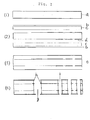
- a shows double-side copper-clad laminate
- b shows copper foil
- c shows prepreg
- d shows circuits
- e shows four-layered board
- f shows penetration hole having a diameter of 100 ⁇ m made with a carbon dioxide gas laser
- g shows penetration hole having a diameter of 150 ⁇ m made with a carbon dioxide gas laser
- h shows copper foil burrs
- i shows copper plating
- j shows flip chip
- k shows bump
- l shows plating resist
- m shows solder ball
- n shows through hole
- o shows blind via hole plated with copper
- p shows position-deviated internal-layer copper foil
- q shows penetration hole plated with copper without a SUEP treatment
- r shows resin layer of a backup sheet
- s shows aluminum foil and t shows auxiliary material layer for making a hole.
- the present invention relates to a high-density printed wiring board in which a double-side copper-clad multi-layered board having at least three copper foil layers is provided with a penetration hole that penetrates through all the copper foil layers and is used for a small-diameter through hole and a method of producing it. Further, the present invention relates to a high-density printed wiring board which is improved in connection properties of a through hole by etching and removing overhanging burrs of the internal-layer copper foil(s) and the front-and-reverse copper foils formed when a hole is made with a carbon dioxide gas laser and carrying out copper plating, and a method of producing it.
- the present invention provides a high-density printed wiring board which achieves the conduction of all the copper foil layers with a small-sized penetration hole, and a method of producing it. While the printed wiring board of the present invention is applicable to a wire-bonding mounting, it is particularly suitable for the mounting of a flip chip.
- a multi-layered copper-clad laminate having at least three copper foil layers is prepared.
- a hole is made in a predetermined position in the above laminate. It is preferred to properly select a method of making a hole depending upon the diameter of a hole. When the diameter of a hole is 25 or more to less than 80 ⁇ m, an excimer laser or a YAG laser is used.
- an auxiliary material of an organic substance containing 3 to 97 % by volume of at least one powder selected from the group consisting of a metal compound powder, a carbon powder and metal powder which have a melting point of at least 900°C and a bond energy of at least 300 KJ/mol is applied on a copper foil surface to form a coating which has a thickness of, preferably, 30 to 100 ⁇ m.
- this resin is attached to a thermosetting film so as to have the total thickness of, preferably, 30 to 200 ⁇ m, the resultant film is disposed on the copper foil surface with the attached-resin facing toward to a copper foil side and, preferably, the resultant set is bonded by laminating.
- the copper foil surface is subjected to an oxidation treatment to form a metal oxide.
- the resultant surface is directly irradiated with a carbon dioxide gas laser having an energy preferably selected from 20 to 60 mJ/pulse to form a penetration hole for a through hole.
- a mechanical drill is preferably used for making a hole.
- the front-and-reverse-layer copper foils may be mechanically polished for removing burrs. However, it is preferred to carry out etching with a chemical from both the front and reverse surfaces for removing burrs of the internal-layer copper foil together.
- the front-and-reverse-layer copper foils are thick, after the formation of a hole, the auxiliary material is removed, the copper foil burrs of the front and reverse layers and the internal layer are removed by etching and at the same time the front-and-reverse-layer copper foils are dissolved and removed partially in the thickness direction to have a thickness of, preferably, 3 to 7 ⁇ m.
- the auxiliary material i.e., resin coating or sheet is left as it is, and an etching solution is blown or sucked at a high rate to dissolve and remove copper foil burrs of the front and reverse layers and the internal layer. Then, the auxiliary material on the front and reverse surfaces is dissolved and removed with a solution in which the resin is soluble.
- the resin of the auxiliary material is selected from resins which are insoluble in the etching solution.
- the use of a copper foil which preferably has an average particle diameter of 1 ⁇ m or less serves to make the formation of a hole with a carbon dioxide gas fine. Then, copper plating is carried out to obtain a double-side copper-clad multi-layered board. Circuits are formed on the front and reverse surfaces of the double-side copper-clad multi-layered board, and a printed wiring board is produced according to a general method.
- the front-and-reverse-layer copper foils preferably have a thickness of 3 to 7 ⁇ m for forming minute circuits on the front and reverse surfaces. When the front-and-reverse-layer copper foils are thin, it becomes possible to produce a high-density printed wiring board without failures such as a short circuit and a pattern breakage.
- oxidation treatment to form a metal oxide on a copper foil surface before the formation of a penetration hole, similarly make a hole with a carbon dioxide gas laser, remove copper foil burrs with a chemical, and dissolve and remove parts of copper foils.
- the processing rate with a carbon dioxide gas laser is remarkably high as compared with the processing rate with a drill, and the method of the present invention is therefore excellent in productivity and excellent in economic performances.
- the multi-layered printed wiring board obtained by making penetration holes, particularly small-diameter holes, for through holes in a copper-clad multi-layered board having at least three copper foil layers, provided by the present invention, is mainly used for mounting a semiconductor chip.
- the multi-layered board used in the present invention is a multi-layered board having at least three copper foil layers which is obtained by making circuits on each layer, surface-treating copper foils thereof as required and laminate-forming the resultant set to integrate it.
- at least one penetration hole having a predetermined diameter is made with a laser to achieve conduction through each of the layers, whereby a printed wiring board is obtained.
- the multi-layered board is not produced with only holes having a diameter of 200 ⁇ m but produced with a combination of at least two kinds of penetration holes having diameters different from each other.
- a substrate having copper foil layers which is the multi-layered board having at least three copper foil layers in the present invention
- a base-reinforced substrate, a film-base substrate, a substrate formed of only a resin without a reinforcing base, etc. may be used.
- a copper-clad multi-layered board formed of a glass fabric substrate is preferred from the viewpoint of a dimensional shrinkage, etc.
- 3 to 7 ⁇ m thick copper foils are provided for surface-layer copper foils from the beginning, or thick copper foils having a thickness of 9 to 18 ⁇ m are provided and subjected to laminate-formation and then the surface-layer copper foils are treated with an etching solution such that the surface-layer copper foils have a thickness of 3 to 7 ⁇ m.
- thin copper foils are used from the beginning, copper foils with a copper or aluminum carrier are mainly used.
- an auxiliary material for making a hole with a carbon dioxide gas laser is preferably used by bonding it on the copper-clad multi-layered board at the time of making a hole.
- a solution of an auxiliary material is applied to a copper foil surface and dried to obtain a coating.
- a varnish is applied to a thermosetting resin and dried to obtain a sheet thereof, and the obtained sheet is used. The sheet is placed on the copper-clad multi-layered board with the resin-bonded surface facing to a copper foil side and the resultant set is laminated under heat and pressure.
- sheets having the resin surface wetted are laminated on the front and reverse surfaces of the copper-clad multi-layered board at room temperature under pressure, whereby adhesion to a copper foil surface becomes excellent and a printed wiring board having holes in an excellent form can be obtained.
- a generally known organic or inorganic woven fabric or non-woven fabric may be used as a substrate for the copper-clad board.
- the inorganic fiber includes fibers of E glass, S glass, D glass and M glass.
- the organic fiber includes fibers of a wholly aromatic polyamide, a liquid crystal polyester and polybenzazole. These may be mixtures.
- a glass fiber woven fabric is used.
- the resin of the thermosetting resin composition of the copper-clad multi-layered board used in the present invention can be selected from generally known thermosetting resins.
- the resin include an epoxy resin, a polyfunctional cyanate ester resin, a polyfunctional maleimide-cyanate ester resin, a polyfunctional maleimide resin and an unsaturated-group-containing polyphenylene ether resin. These resins are used alone or in combination.
- a thermosetting resin composition having a glass transition temperature of at least 150°C.
- a polyfunctional cyanate ester resin composition In view of humidity resistance, anti-migration properties and electric characteristics after moisture absorption, it is preferred to use a polyfunctional cyanate ester resin composition. Further, for improving the form of a hole, a generally-known inorganic filler is added, and further, it is preferred to add a black dye or pigment.
- a polyfunctional cyanate ester compound which is a suitable thermosetting resin component in the present invention refers to a compound having at least 2 cyanato groups per molecule. Specific examples thereof include 1,3- or 1,4-dicyanatobenzene, 1,3,5-tricyanotobenzene, 1,3-, 1,4-, 1,6-, 1,8-, 2,6- or 2,7-dicyanatonaphthalene, 1,3,6-tricyanatonaphthalene, 4,4-dicyanatobiphenyl, bis (4-dicyanatophenyl)methane, 2,2-bis (4-cyanatophenyl)propane, 2,2-bis(3,5-dibromo-4-cyanatophenyl)propane, bis(4-cyanatophenyl) ether, bis(4-cyanatophenyl)thioether, bis (4-cyanotophenyl) sulfone, tris (4-cyanatophenyl)phosphite, tris(4-cyanatopheny
- polyfunctional cyanate ester compounds disclosed in Japanese Patent Publications Nos. 41-1928, 43-18468, 44-4791, 45-11712, 46-41112 and 47-26853 and JP-A-51-63149. Further, there may be used a prepolymer having a molecular weight of 400 to 6,000 and having a triazine ring formed by trimerizing cyanato group of any one of these polyfunctional cyanate ester compounds.
- the above prepolymer is obtained by polymerizing the above polyfunctional cyanate ester monomer in the presence of an acid such as a mineral acid or a Lewis acid, a base such as sodium alcoholate or tertiary amine, or a salt such as sodium carbonate, as a catalyst.
- the prepolymer partially contains unreacted monomer and is in the form of a mixture of a monomer and a prepolymer, and the prepolymer in the above form is also suitably used in the present invention. Generally, it is dissolved in an organic solvent in which it is soluble, before use.
- the epoxy resin is generally selected from known epoxy resins. Specific examples thereof include a liquid or solid bisphenol A type epoxy resin, a bisphenol F type epoxy resin, a phenol novolak type epoxy resin, a cresol novolak type epoxy resin, an alicyclic epoxy resin, a polyepoxy compound obtained by epoxidizing the double bond of butadiene, pentadiene, vinylcyclohexene or dicyclopentyl ether, a polyol, and a polyglycidyl compound obtained by a reaction between a hydroxyl-group-containing silicone resin and epohalohydrin. These resins may be used alone or in combination.
- thermosetting resin composition in the present invention so long as the inherent properties of the composition are not impaired.
- the above additives include monomers having polymerizable double bonds such as unsaturated polyester, prepolymers of these, liquid elastic rubbers having a low molecular weight or elastic rubbers having a high molecular weight such as polybutadiene, epoxidized butadiene, maleated butadiene, a butadiene-acrylonitrile copolymer, polychloroprene, a butadiene-styrene copolymer, polyisprene, butyl rubber, fluorine rubber and natural rubber, polyethylene, polypropylene, polybutene, poly-4-methylpentene, polystyrene, AS resin, ABS resin, MBS resin, styrene-isoprene rubber, a polyethylene-propylene copolymer, a 4-fluoroethylene-6-flucroethylene copolymer, high-molecular-
- thermosetting resin composition used in the present invention undergoes curing itself under heat.
- a known heat-curing catalyst may be incorporated into the thermosetting resin.
- the amount of the catalyst per 100 parts by weight of the thermosetting resin is 0.005 to 10 parts by weight, preferably 0.01 to 5 parts by weight.
- the metal compound having a melting point of at least 900°C and a bond energy of at least 300 kJ/mol, used in an auxiliary material in the present invention can be generally selected from known metal compounds.
- oxides are used.
- the oxides include titanias such as titanium oxide, magnesias such as magnesium oxide, oxides of iron such as iron oxide, oxides of nickel such as nickel oxide, manganese dioxide, oxides of zinc such as zinc oxide, silicon dioxide, aluminum oxide, rare earth metal oxides, oxides of cobalt such as cobalt oxide, oxides of tin such as tin oxide and oxides of tungsten such as tungsten oxide.
- non-oxides may be used.
- the non-oxides include generally known non-oxides such as silicon carbide, tungsten carbide, boron nitride, silicon nitride, titanium nitride, aluminum nitride, barium sulfate and rare earth metal sulfides.
- carbon may be used.
- various glasses which are mixtures of metal oxide powders may be also used.
- a carbon powder may be used.
- powders of simple substances of silver, aluminum, bismuth, cobalt, copper, iron, magnesium, manganese, molybdenum, nickel, palladium, antimony, silicon, tin, titanium, vanadium, tungsten and zinc or metal powders of alloys of these may be used. These are used alone or in combination.
- the particle diameter of these is not specially limited, while it is preferably 1 ⁇ m or less.
- a powder containing Na, K or Cl ion is not preferred since it has a detrimental effect on the reliability of a semiconductor.
- the amount of the above powder is 3 to 97 % by volume, preferably 5 to 95 % by volume.
- the above powder is incorporated into a resin composition and homogeneously dispersed.
- 3 to 7 ⁇ m thick copper foils are provided for surface-layer copper foils from the beginning, or thick copper foils having a thickness of 9 to 18 ⁇ m are provided and subjected to laminate-formation, and then, the surface-layer copper foils are treated with an etching solution such that the surface-layer copper foils have a thickness of 3 to 7 ⁇ m.
- thin copper foils are used from the beginning, copper foils with a copper or aluminum carrier are mainly used.
- the resin used in an auxiliary material is preferably selected from water-soluble resins, when the front-and reverse layer copper foils are thick. Specifically, water-soluble polyester resins, acrylate resins, polyether resins, polyvinyl alcohol resins, and starch are used. Also in this case, various additives may be added. The additives are selected and incorporated such that the additives are not dissolved or peeled off in an etching step.
- the resin is selected from resins which are insoluble in an etching solution. After bonding the auxiliary material to a copper-clad multi-layered board, it is also possible to cure the resin with ultraviolet, etc., so as not to dissolve in the etching solution.
- an acid resin composition which is insoluble in water but is soluble in an organic solvent is used.
- thermosetting film When a thermosetting film is attached, the film is peeled off after etching and the acid resin is dissolved and removed with an alkaline solution or an organic solvent.
- a resin which is soluble in the solvent, other than the acid resin composition may be used.
- the resin layers on the front and reverse surfaces are dissolved and removed with an organic solvent after the formation of holes and the removal of burrs.
- an acid resin composition which can be removed with an alkaline aqueous solution, as an auxiliary material.
- the method of preparing composition containing a metal compound powder, a carbon powder or a metal powder and a resin and the method of forming it in a sheet are not critical.
- the above methods include known methods such as a method of kneading materials without any solvent at a high temperature with a kneader and extruding the kneaded mixture in the form of a sheet to bond it to a thermoplastic film surface, and a method of dissolving a resin in a solvent, adding the above powder thereto, homogeneously mixing them with stirring, applying the mixture as a coating composition to a copper foil surface and drying it to form a coating or applying it to a thermoplastic film surface and drying it to form a coating.
- the thickness is not specially limited. However, when the coating composition is applied, the thickness of a coating is preferably 30 to 100 ⁇ m. When the above composition is applied to a film to form a coating with a film, the total thickness is preferably arranged to be 30 to 200 ⁇ m
- the above auxiliary sheet is laminated on a copper foil surface under heat and pressure, the applied resin layer side thereof is attached to the copper foil surface, and the auxiliary sheet is laminated on the copper foil surface with a roll by melting the resin layer at a temperature generally between 40°C and 150°C, preferably between 60°C and 120°C at a linear pressure of generally 0.5 to 20 kgf/cm, preferably 1 to 10 kgf/cm to attach the resin layer to the copper foil surface closely.
- the temperature to be employed differs depending upon the melting point of a selected water-soluble resin and also differs depending upon a selected linear pressure and a laminating rate. Generally, the lamination is carried out at a temperature higher than the melting point of the water-soluble resin by 5 to 20°C.
- oxidation treatment to form a metal oxide a generally known treatment may be used. Further, there may be employed a treatment with a chemical, e.g., Meck CZ treatment with CZ8000, supplied by Meck K.K..
- the reinforced copper-clad multi-layered board is prepared as follows. First, the above reinforcing material is impregnated with the thermosetting resin composition, and the impregnated reinforcing material is dried to B-stage the composition, whereby a prepreg is obtained. A predetermined number of the prepreg sheets are stacked, a copper foil is placed on at least one surface of the stacked prepreg sheets, and the resultant set is laminate-formed under heat and pressure to form a copper-clad multi-layered board having at least three copper layers.
- the copper foil as an outer layer preferably has a thickness of 3 to 12 ⁇ m and the copper foil as an internal layer has a thickness of 9 to 18 ⁇ m.
- a copper-clad multi-layered board is used as a multi-layered board.
- the copper-clad multi-layered board is prepared by forming a circuit in a copper-clad laminate preferably having a reinforced base material, treating a copper foil surface, then, arranging a B-staged prepreg having a reinforced base material or a resin sheet having no base material, a copper foil having a resin attached thereto and a resin layer formed by the application of a coating composition on at least one surface, placing a copper foil or copper foils on outermost surface or surfaces and laminate-forming the resultant set under heat and under pressure, preferably in vacuum.
- the method of removing the copper burrs occurring on the hole portions by etching is not specially limited, and it includes methods of dissolving and removing a metal surface with a chemical (called a SUEP method) disclosed, for example, in JP-A-02-22887, JP-A-02-22896, JP-A-02-25089, JP-A-02-25090, JP-A-02-59337, JP-A-02-60189, JP-A-02-166789, JP-A-03-25995, JP-A-03-60183, JP-A-03-94491, JP-A-04-199592 and JP-A-04-263488.
- a SUEP method a chemical
- the etching is generally carried out at a rate of 0.02 to 1.0 ⁇ m/second.
- the blowing angle and pressure of an etching solution are properly selected.
- a carbon dioxide gas laser generally uses a wavelength of 9.3 to 10.6 ⁇ m in an infrared wavelength region. While the output thereof is not specially limited, the copper foils and an insulation layer are processed by irradiation of required pulses (shots) by means of a pulse oscillation preferably at an energy of 20 to 60 mJ/pulse to make holes.
- shots required pulses
- a pulse oscillation preferably at an energy of 20 to 60 mJ/pulse to make holes.
- the penetration hole there may be employed any method, i.e., a method in which irradiation with an energy selected from 20 to 60 mJ/pulse is carried out from beginning to end and a method in which a hole made in the copper foil and then the insulation layer is processed with a decreased energy.
- a metal sheet is preferably disposed thereon with part of the metal sheet bonding to the resin, penetration holes for through holes are made, then, the metal sheet is peeled off, copper foil burrs in circumferential regions of the holes on the front and reverse surfaces and internal copper foil burrs are removed by etching with retaining the resin layers on the front and reverse surfaces as they are, and then the resin layers are dissolved and removed.
- the front-and-reverse-layer copper foils are thick, the auxiliary material on the front and reverse surfaces or oxidation treatment to form a metal oxide is removed after the formation of holes and etching is carried out.
- An excimer laser generally uses a wavelength of 248 to 308 nm.
- An YAG laser generally uses a wavelength of 351 to 355 nm.
- the method of processing holes is not limited.
- the wavelength is not necessarily limited.
- a resin layer having a thickness of about 1 ⁇ m remains on the internal sides of the front and reverse layers and an internal copper foil surface in the inside of the processed hole.
- the above resin layer can be removed according to a known treatment such as a desmear treatment before etching.
- a solution does not reach to the inside of a small-diameter hole, the remains of the resin layer remaining on the internal layer copper foil surface occur, which sometimes cause a failure in connection to copper plating. Therefore, more preferably, first, the inside of a hole is treated in a gaseous phase to remove the remaining resin layer completely and then the copper foil burrs of the inside of a hole and the front and reverse surfaces are removed by etching.
- the gaseous phase treatment can be selected from known methods such as plasma treatment and treatment with low-pressure ultraviolet light.
- the plasma treatment uses low-temperature plasma prepared by partially exciting and ionizing molecules with a high-frequency power source. In the plasma treatment, a high-rate treatment using ionic impact or a moderate treatment with radical species is generally used.
- a processing gas a reactive gas or an inert gas is used.
- oxygen is mainly used.
- a surface is chemically treated.
- argon gas is mainly used.
- Physical surface treatment is carried out with argon gas, or the like. The physical treatment physically cleans a surface with an ionic impact.
- the low-pressure ultraviolet light is ultraviolet light in a short wavelength region.
- a resin layer is decomposed and removed by irradiation with ultraviolet light in a short wavelength region having a peak at 184.9 nm or 253.7 nm. While the inside of a hole may be treated by a general copper plating, part, preferably at least 80 % by volume, of the inside of a hole may be filled with copper plating.
- a through hole penetration hole is made without deviations of a hole from land copper foils on front and reverse surfaces of a copper-clad board at a remarkably higher rate as compared with the processing rate with a mechanical drill, and productivity is also remarkably improved.
- Copper foils on both surfaces are two-dimensionally etched to remove parts of the thickness of copper foils as raw materials, whereby copper foil burrs occurring in hole portions are concurrently etched and removed.
- a high-density printed wiring board which is free from the occurrence of a short circuit and a pattern breakage when front-surface and reverse-surface circuits are formed by copper plating in a step to follow and which has excellent reliability.
- a catalyst 0.4 part of zinc octylate was added, and these materials were dissolved and mixed.
- an inorganic filler (trade name: Calcined Talc, supplied by Nippon Talc K.K.) and 8 parts of a black pigment, and these materials were homogeneously stirred and mixed to prepare a varnish A.
- the above varnish was used to impregnate a 100 ⁇ m thick glass woven fabric, and the impregnated glass woven fabric was dried at 150°C to prepare prepreg B having a gelation time of 120 second at 170°C and having a glass fabric content of 56 % by weight. Further, there was prepared Prepreg C having a glass content of 44 % by weight.
- Circuits were formed on the front and reverse surfaces of the laminate, the copper foil surfaces were treated to form black copper oxide, the above prepregs C were placed on the upper and lower surfaces, one on one surface and the other on the other surface, and 12 ⁇ m thick electrolytic copper foils having an average particle diameter of 3 ⁇ m were placed thereon, and the resultant set was similarly laminate-formed to obtain a multi-layered board E having four layers (Fig.1 (2), (3)).
- a copper oxide powder (average particle diameter: 0.9 ⁇ m) as a metal compound powder was added to a varnish of polyvinyl alcohol in water, and these materials were homogeneously stirred and mixed to obtain a varnish F.
- the varnish F was applied to one surface of a 50 ⁇ m thick polyethylene terephthalate film to form a coating having a thickness of 25 ⁇ m, and the coating was dried to obtain an auxiliary material G having a metal compound content of 35 % by volume.
- the above varnish F was applied on a 50 ⁇ m thick aluminum, to form a coating having a thickness of 25 ⁇ m, and the coating was dried to obtain a backup sheet H for a reverse surface.
- the auxiliary material G was disposed on the upper surface of the laminate E, the backup sheet H was disposed on the lower surface of the laminate E, and the resultant set was laminated at 100 °C under a pressure of 2kgf/cm.
- the above laminate surface was 1 shot irradiated directly with a carbon dioxide gas laser at an output of 40 mJ/pulse and then 6 shots irradiated at an output of 28 mJ/pulse, to form 144 penetration holes having a diameter of 100 ⁇ m each for through holes in each of 70 blocks in a central flip-chip-mounting portion having a size of 6 mm x 6 mm in a 50 mm x 50mm square area.
- 100 penetration holes having a diameter of 150 ⁇ m were similarly made in a circumferential region of the flip-chip-mounting portion with a carbon dioxide gas laser (Fig.1 (4)).
- the resin layer of the auxiliarymaterial on the front surface was peeled off, then, the resultant board was placed and treated in a plasma apparatus, and then a SUEP solution was sucked at a high rate to arrange the thickness of the front and reverse copper foils to be 4 ⁇ m and at the same time dissolve and remove burrs of the internal and outer layers.
- a SUEP solution was sucked at a high rate to arrange the thickness of the front and reverse copper foils to be 4 ⁇ m and at the same time dissolve and remove burrs of the internal and outer layers.
- copper was plated on the resultant board to form a 15 ⁇ m thick plating layer.
- 93 % by volume of the inside of each hole was filled (Fig.2 (5)).
- circuits (144, line/space 70/70 ⁇ m), bonding pads and pads for solder balls, etc., were formed according to a conventional method, portions other than at least the bonding pads and the solder ball pads were coated with a plating resist, and nickel plating and gold plating were carried out to obtain a printed wiring board.
- a flip chip was mounted on the printed wiring board, and solder balls were bonded to the reverse surface to obtain a semiconductor plastic package (Fig.2(6)).
- Tables 1 and 2 show the evaluation results to the printed wiring board.
- a metal compound powder (SiO 2 : 57 wt%, MgO: 43 wt%, average particle diameter: 4 ⁇ m) was added to a solution of carboxyl-group-containing polyester resin having a melting point of 67°C and an acid value of 71mgKOH/g in n-butanol, and these materials were homogeneously mixed and stirred to obtain a varnish I.
- one prepreg which was the same as the prepreg C in Example 1 was used, 12 ⁇ m thick electrolytic copper foils having an average particle diameter of 1 ⁇ m were placed on upper and lower surfaces of the prepreg, and the resultant set was similarly laminate formed, to give a double-side copper-clad laminate. Circuits were formed on the front and reverse surfaces of the obtained board, and then, the surfaces were treated to form black copper oxide. Then, sheets of the above prepreg C were placed on the upper and lower surfaces of the laminate, one sheet on one surface and one sheet on the other surface, 7 ⁇ m thick electrolytic copper foils were placed thereon, and the resultant set was similarly laminate-formed to obtain a four-layered board J.
- a hole-filling resin (trade name; BT-S730B, supplied by Mitsubishi Gas Chemical Company, INC.) was filled therein and cured at 110 °C for 1 houre and then at 160°C for 3 hours, and then, resins remaining on the surfaces were removed by polishing.
- the above varnish I was applied to the front and reverse surfaces of the four-layered board and dried to form coatings having a thickness of 50 ⁇ m, a release agent-attached aluminum was disposed on the outer side of the reverse surface, the board surface was 5 shots irradiated with a carbon dioxide gas laser at an output of 35 mJ/pulse, to make penetration holes having a diameter of 100 ⁇ m each in the same form in which the penetration holes penetrated through the internal layer copper foils as in Example 1. The aluminum was peeled off with retaining the resin layer on the reverse surface.
- Example 2 The same double-side copper-clad laminate as that in Example 2 was provided, and attempts were made similarly to make holes in the laminate with a carbon dioxide gas laser with attaching nothing on the surface of the laminate. No holes were made.
- the same multi-layered board E as that in Example 1 was provided.
- the copper foil on the front surface was blackened with a magic marker.
- the blackened surface was irradiated with the same number of shots of a carbon dioxide gas laser at an energy of 40 mJ/pulse in order to make holes having a diameter of 100 ⁇ m. No holes were made in the copper foil.
- the resultant laminate was treated to form black copper oxide, then, sheets of prepreg M were placed on both the surfaces, one sheet on one surface and one sheet on the other surface thereof, copper foils having a thickness of 12 ⁇ m and an average particle diameter of 3 ⁇ m were placed thereon, and the resultant set was similarly laminate-formed.
- 144 holes having a diameter of 150 ⁇ m each for forming via holes were made within a semiconductor-chip-mounting area on the front surface and a corresponding area on the reverse surface which have a 6 mm x 6 mm square size by the removal of the copper foils by means of etching.
- the surface was 3 shots irradiated with a carbon dioxide gas laser at an energy of 15 mJ/pulse to similarly form 100 via holes having the same diameter in a circumferential region of the semiconductor flip-chip-mounting portion and a corresponding circumferential region on the reverse surface. Then, desmear treatment was carried out without the SUEP treatment and a gaseous phase treatment, and a general copper plating was carried out to obtain a printed wiring board similarly (Fig.4 (3)). A flip chip was mounted to obtain a semiconductor plastic package. Tables 1 and 2 show the evaluation results to the printed wiring board.
- Example 2 The same multi-layered board E as that in Example 1 was provided, and penetration holes were similarly made with a mechanical drill having a drill diameter of 250 ⁇ m at 100,000 rpm.
- One desmear treatment was carried out without the SUEP treatment, followed by copper plating according to a general method, to complete a printed wiring board.
- Tables 1 and 2 show the evaluation results to the printed wiring board.
- Example 1 the double-side copper-clad laminate D was used, copper foils on portions where through holes of internal layers were to be formed on the front and reverse surfaces of the laminate D were etched so as to have a hole diameter of 100 ⁇ m, circuits were formed, then, copper foil surfaces were treated to form black copper oxide, sheets of prepreg C were placed thereon, 12 ⁇ m thick electrolytic copper foils having an average particle diameter of 3 ⁇ m were placed thereon, and the resultant set was laminate-formed under the same conditions as those in Example 1, to prepare a four-layered board (Fig.5 (1)). This multi-layered board was used, and holes having a diameter of 100 ⁇ m were made in positions where penetration holes were to be formed on the front surface by etching the copper foil.
- penetration holes ?? having a diameter of 100 ⁇ m were also made in the same positions on the reverse surface.
- the front surface was 6 shots irradiated with a carbon dioxide gas laser at an output of 15 mJ/pulse to form penetration holes for through holes (Fig.5 (2)).
- one desmear treatment was carried out without the SUEP treatment in the same manner as in Comparative Example 4, copper plating was carried out to form a 15 ⁇ m thick plating layer (Fig.5 (3)), and circuits were formed on the front and reverse surfaces, whereby a printed wiring board was similarly obtained.
- Tables 1 and 2 show the evaluation results to the printed wiring board.
- a land having a diameter of 350 ⁇ m was formed in each through hole, and 900 holes were connected alternately from one surface to the other surface or from one upper via hole to one lower via hole.
- One heat cycle consisted of immersion for soldering at 260°C for 30 seconds and standing at room temperature for 5 minutes, and 200 cycles were repeated. Table 1 shows the maximum value of change ratios of resistance values.
- a land having a diameter of 350 ⁇ m is formed around a hole and, at that time, copper foil hiatuses in a land portion are observed.
- Fifty through holes having a diameter of 100 ⁇ m or less and having a hole-hole distance of 150 ⁇ m were independently connected in parallel, and 100 sets of such connections were made. These sets were treated at 130°C at 85 %RH under 1.8 VDC for a predetermined period of time, taken out and measured for an insulation resistance value between the through holes.
- a metal compound powder (SiO 2 : 57 wt%, MgO: 43 wt%, average particle diameter: 4 ⁇ m) was added to a solution of water-insoluble polyester resin having a melting point of 55°C in methyl ethyl ketone, and these materials were homogeneously mixed and stirred, and the mixture was applied to one surface of a 50 ⁇ m thick polyethylene terephthalate film to form a coating having a thickness of 85 ⁇ m. The coating was dried at 110°C for 25 minutes to obtain a film-like auxiliary material O having a metal compound content of 15 % by volume.
- one sheet of the same prepreg C as that in Example 1 was provided, 18 ⁇ m thick electrolytic copper foils were placed on the upper and lower surfaces of the above prepreg, and the resultant set was similarly laminate-formed to obtain a double-side copper-clad laminate. Circuits were formed on the front and reverse surfaces of the laminate and then the surfaces were treated to form a black copper oxide. Then, sheets of the above prepreg C were placed on the upper and lower surfaces of the laminate, one sheet on one surface and one sheet on the other surface, 7 ⁇ m thick electrolytic copper foils were placed thereon, and the resultant set was similarly laminate-formed to obtain a four-layered board P.
- the above polyester solution was applied on one surface of a 50 ⁇ m thick aluminum to form a coating having a thickness of 20 ⁇ m, and the coating was dried to obtain a coating-attached aluminum, which was to be used as a backup sheet Q.
- the above hole-making auxiliary material O was disposed on the four-layered board P and the backup sheet Q was disposed on the other surface of the four-layered board P while their resin surfaces faced toward the copper foil sides.
- the resultant set was laminated at 80°C at a linear pressure of 1.5 kgf/cm, to obtain a coating-sheet-attached four-layered board having excellent adhesion (step (1) in Fig.3).
- the front surface was 5 shots irradiated with a carbon dioxide gas laser at an output of 35 mJ/pulse to form penetration holes in the form in which the penetration holes perforated through the internal copper foils (step (2) in Fig.3).
- the aluminum was peeled off with retaining the resin layer on the reverse surface, and an etching solution was passed through the insides of the holes made at a high rate with retaining the auxiliary sheet on the front surface, to remove copper foil burrs of the surface-layers and internal layers (step (3) in Fig.3) .
- Example 3 shows the evaluation results to the printed wiring board.
- Example 3 Deviation of land copper foils on the front and reverse surfaces ( ⁇ m) 0 Deviation of hole positions from the internal layer ( ⁇ m) - Pattern breakage and short circuit (number) 0/200 Copper foil hiatuses around land Nil Glass transition temperature (°C) 235 Through hole and via hole-heat cycle test (%) 100 cycles 1.3 200 cycles 1.4 500 cycles 1.5 Processing time period for making holes (minute) 16
- Circuits were formed on the front and reverse surfaces of the laminate, copper foil surfaces were treated to form black copper oxide, the same prepregs C as that in Example 1 were placed on the upper and lower surfaces of the laminate, one on one surface and the other on the other surface, and 7 ⁇ m thick electrolytic copper foils were placed thereon, and the resultant set was laminate-formed under the same conditions as above to obtain a multi-layered board S having four layers.
- the above acrylate resin solution was applied on the other surface so as to form a coating having a thickness of 50 ⁇ m, and similarly dried to obtain a coating V.
- 100 ⁇ m thick aluminum was disposed on the outer side of the coating V, the auxiliary material layer U was 1 shot irradiated directly with a carbon dioxide gas laser at an output of 40 mJ/pulse and then 7 shots irradiated at an output of 28 mJ/pulse, to form 900 penetration holes having a diameter of 100 ⁇ m each for through holes in each of 70 blocks , 63,000 holes in total, in a 50 mm x 50mm square area.
- the aluminum on the reverse surface was removed, the resin layer of the auxiliary material on the front surface was retained as it was, the resultant board was placed and treated in a plasma apparatus, and then a SUEP solution was blown at a high rate to remove burrs of the front-and-reverse and internal layers.
- the acid resins on the front and reverse surfaces were dissolved and removed with a sodium hydroxide aqueous solution. After desmear treatment, copper was plated on the resultant board to form a 15 ⁇ m thick plating layer.
- circuits (200, line/space 70/70 ⁇ m) and pads for solder balls, etc., were formed according to a conventional method, portions other than at least a semiconductor chip portion, a pad portion for bonding and a solder ball pad portion were coated with a plating resist, and nickel plating and gold plating were carried out to obtain a printed wiring board.
- Table 4 shows the evaluation results to the printed wiring board.
- a metal compound powder (SiO 2 : 57 wt%, MgO: 43 wt%, average particle diameter: 4 ⁇ m) was added to a solution of a carboxyl-group-containing polyester resin having a melting point of 67°C and an acid value of 71 mgKOH/g in n-butanol, and these materials were homogeneously mixed and stirred, and the mixture was applied to one surface of a 50 ⁇ m thick polyethylene terephthalate film to form a coating having a thickness of 85 ⁇ m. The coating was dried at 110°C for 25 minutes to obtain a film-like auxiliary material W having a metal compound content of 85 % by volume.
- Example 2 Separately, one sheet of the same prepreg C as that in Example 1 was provided, 18 ⁇ m thick electrolytic copper foils having an average particle diameter of 0.5 ⁇ m were placed on the upper and lower surfaces of the above prepreg, and the resultant set was laminate-formed under the same conditions as those in Example 5, to obtain a double-side copper-clad laminate. Circuits were formed on the front and reverse surfaces of the laminate and then the surfaces were treated to form a black copper oxide.
- the above polyester solution was applied to the reverse surface of the four-layered board and dried to form a coating having a thickness of 50 ⁇ m, and a release agent-attached aluminum having a thickness of 100 ⁇ m was disposed on the outer side thereof.
- the above hole-making auxiliary material W was disposed on the front surface with the resin side facing toward the copper foil side, and the resultant set was laminated at 100°C at a linear pressure of 5 kgf/cm, to make the aluminum and the auxiliary material adhere to the four-layered board.
- the front surface was 5 shots irradiated with a carbon dioxide gas laser at an output of 35 mJ/pulse to form penetration holes in the form in which the penetration holes perforated through the internal copper foils.
- the aluminum was peeled off with retaining the resin layer on the reverse surface, and an acid etching solution was passed through the insides of the holes made at a high rate by suction with retaining the auxiliary sheet on the front surface, to remove copper foil burrs of the surface-layers and internal layers.
- Example 4 Deviation of land copper foils on the front and reverse surfaces ( ⁇ m) 0 0 Deviation of hole positions from the internal layer ( ⁇ m) 0 - Pattern breakage and short circuit (number) 0/200 0/200 Copper foil hiatuses around land Nil Nil Glass transition temperature (°C) 235 235 Through hole-heat cycle test (%) 100 cycles 1.1 1.3 200 cycles 1.2 1.4 500 cycles 1.4 1.5 Processing time period for making holes (minute) 24 16 Migration resistance (HAST) ( ⁇ ) Ordinary state 2x10 11 - 200 hours 8x10 8 500 hours 8x10 8 700 hours 7x10 8 1000 hours 7x10 8
Landscapes
- Engineering & Computer Science (AREA)
- Physics & Mathematics (AREA)
- Optics & Photonics (AREA)
- Manufacturing & Machinery (AREA)
- Microelectronics & Electronic Packaging (AREA)
- Production Of Multi-Layered Print Wiring Board (AREA)
- Laser Beam Processing (AREA)
Applications Claiming Priority (6)
| Application Number | Priority Date | Filing Date | Title |
|---|---|---|---|
| JP17164299A JP4727013B2 (ja) | 1999-06-17 | 1999-06-17 | 炭酸ガスレーザー加工によるスルーホールを有する多層プリント配線板の製造方法 |
| JP17164499 | 1999-06-17 | ||
| JP17164499A JP2001007535A (ja) | 1999-06-17 | 1999-06-17 | 信頼性に優れたスルーホールを有する多層プリント配線板の製造方法 |
| JP17164299 | 1999-06-17 | ||
| JP11171645A JP2001007478A (ja) | 1999-06-17 | 1999-06-17 | 信頼性に優れたスルーホールを有する高密度多層プリント配線板 |
| JP17164599 | 1999-06-17 |
Publications (3)
| Publication Number | Publication Date |
|---|---|
| EP1061785A2 true EP1061785A2 (fr) | 2000-12-20 |
| EP1061785A3 EP1061785A3 (fr) | 2001-12-05 |
| EP1061785B1 EP1061785B1 (fr) | 2010-07-28 |
Family
ID=27323514
Family Applications (1)
| Application Number | Title | Priority Date | Filing Date |
|---|---|---|---|
| EP00305072A Expired - Lifetime EP1061785B1 (fr) | 1999-06-17 | 2000-06-15 | Circuit imprimé multicouche à haute densité ayant des trous traversants à haute fiabilité et procédé de fabrication de ce circuit imprimé |
Country Status (3)
| Country | Link |
|---|---|
| US (1) | US6708404B1 (fr) |
| EP (1) | EP1061785B1 (fr) |
| DE (1) | DE60044736D1 (fr) |
Cited By (4)
| Publication number | Priority date | Publication date | Assignee | Title |
|---|---|---|---|---|
| WO2010078611A1 (fr) * | 2009-01-09 | 2010-07-15 | At & S Austria Technologie & Systemtechnik Aktiengesellschaft | Carte de circuit imprimé comprenant au moins un élément d'arrêt de faisceau laser, et procédé de fabrication de ladite carte |
| CN109640518A (zh) * | 2019-01-30 | 2019-04-16 | 无锡深南电路有限公司 | 激光成孔方法、覆铜板和电路板 |
| RU223981U1 (ru) * | 2023-12-06 | 2024-03-11 | Российская Федерация, от имени которой выступает ФОНД ПЕРСПЕКТИВНЫХ ИССЛЕДОВАНИЙ | Радиоэлектронный блок |
| CN117881112A (zh) * | 2024-03-12 | 2024-04-12 | 四川英创力电子科技股份有限公司 | 一种28层8阶Ultra HDI及其制作方法 |
Families Citing this family (17)
| Publication number | Priority date | Publication date | Assignee | Title |
|---|---|---|---|---|
| US7140103B2 (en) * | 2001-06-29 | 2006-11-28 | Mitsubishi Gas Chemical Company, Inc. | Process for the production of high-density printed wiring board |
| US6826830B2 (en) * | 2002-02-05 | 2004-12-07 | International Business Machines Corporation | Multi-layered interconnect structure using liquid crystalline polymer dielectric |
| US6943446B2 (en) * | 2002-11-08 | 2005-09-13 | Lsi Logic Corporation | Via construction for structural support |
| WO2006080073A1 (fr) * | 2005-01-27 | 2006-08-03 | Matsushita Electric Industrial Co., Ltd. | Substrat de circuit a couches multiples et procede de fabrication |
| JP2006278774A (ja) * | 2005-03-29 | 2006-10-12 | Hitachi Cable Ltd | 両面配線基板の製造方法、両面配線基板、およびそのベース基板 |
| KR101277390B1 (ko) * | 2005-05-31 | 2013-06-20 | 히다치 비아 메카닉스 가부시키가이샤 | 프린트 배선판의 제조방법 및 그것에 이용되는 동박을 붙인 적층판 및 처리액 |
| JP4287458B2 (ja) * | 2005-11-16 | 2009-07-01 | サムソン エレクトロ−メカニックス カンパニーリミテッド. | ペーストバンプを用いた印刷回路基板およびその製造方法 |
| US7605343B2 (en) * | 2006-05-24 | 2009-10-20 | Electro Scientific Industries, Inc. | Micromachining with short-pulsed, solid-state UV laser |
| TW200810637A (en) * | 2006-08-10 | 2008-02-16 | Nan Ya Printed Circuit Board Corp | Method for forming micro blind via on a copper clad laminate substrate utilizing laser drilling technique |
| US7605460B1 (en) * | 2008-02-08 | 2009-10-20 | Xilinx, Inc. | Method and apparatus for a power distribution system |
| US10194537B2 (en) | 2013-03-25 | 2019-01-29 | International Business Machines Corporation | Minimizing printed circuit board warpage |
| ITPI20130044A1 (it) * | 2013-05-24 | 2014-11-25 | Marco Ariani | Struttura perfezionata di supporto per articoli di vario genere |
| CN104349609A (zh) * | 2013-08-08 | 2015-02-11 | 北大方正集团有限公司 | 印刷线路板及其制作方法 |
| JP6350062B2 (ja) * | 2013-10-09 | 2018-07-04 | 日立化成株式会社 | 多層配線基板の製造方法 |
| JP6350064B2 (ja) | 2013-10-09 | 2018-07-04 | 日立化成株式会社 | 多層配線基板の製造方法 |
| JP6327463B2 (ja) | 2013-10-09 | 2018-05-23 | 日立化成株式会社 | 多層配線基板の製造方法 |
| TWI704852B (zh) * | 2018-11-28 | 2020-09-11 | 先豐通訊股份有限公司 | 電路板的電鍍方法及其所製成的電路板 |
Family Cites Families (5)
| Publication number | Priority date | Publication date | Assignee | Title |
|---|---|---|---|---|
| GB1174043A (en) * | 1966-03-01 | 1969-12-10 | British Aircraft Corp Ltd | Improvements relating to the manufacture of Printed Circuits |
| DE3103986A1 (de) | 1981-02-05 | 1982-09-09 | Reiner Dipl.-Phys. 8011 Vaterstetten Szepan | Verfahren zur herstellung von bohrloechern zur durchkontaktierung in elektronischen leiterplatten |
| EP1796446B1 (fr) * | 1996-11-20 | 2011-05-11 | Ibiden Co., Ltd. | Circuit imprimé |
| KR100637904B1 (ko) | 1998-03-18 | 2006-10-24 | 미쯔비시 가스 케미칼 컴파니, 인코포레이티드 | 레이저에 의한 관통홀 제조방법 |
| US6280641B1 (en) * | 1998-06-02 | 2001-08-28 | Mitsubishi Gas Chemical Company, Inc. | Printed wiring board having highly reliably via hole and process for forming via hole |
-
2000
- 2000-06-14 US US09/593,494 patent/US6708404B1/en not_active Expired - Lifetime
- 2000-06-15 EP EP00305072A patent/EP1061785B1/fr not_active Expired - Lifetime
- 2000-06-15 DE DE60044736T patent/DE60044736D1/de not_active Expired - Lifetime
Non-Patent Citations (1)
| Title |
|---|
| None |
Cited By (6)
| Publication number | Priority date | Publication date | Assignee | Title |
|---|---|---|---|---|
| WO2010078611A1 (fr) * | 2009-01-09 | 2010-07-15 | At & S Austria Technologie & Systemtechnik Aktiengesellschaft | Carte de circuit imprimé comprenant au moins un élément d'arrêt de faisceau laser, et procédé de fabrication de ladite carte |
| CN109640518A (zh) * | 2019-01-30 | 2019-04-16 | 无锡深南电路有限公司 | 激光成孔方法、覆铜板和电路板 |
| CN109640518B (zh) * | 2019-01-30 | 2024-03-15 | 无锡深南电路有限公司 | 激光成孔方法、覆铜板和电路板 |
| RU223981U1 (ru) * | 2023-12-06 | 2024-03-11 | Российская Федерация, от имени которой выступает ФОНД ПЕРСПЕКТИВНЫХ ИССЛЕДОВАНИЙ | Радиоэлектронный блок |
| CN117881112A (zh) * | 2024-03-12 | 2024-04-12 | 四川英创力电子科技股份有限公司 | 一种28层8阶Ultra HDI及其制作方法 |
| CN117881112B (zh) * | 2024-03-12 | 2024-05-07 | 四川英创力电子科技股份有限公司 | 一种28层8阶Ultra HDI及其制作方法 |
Also Published As
| Publication number | Publication date |
|---|---|
| DE60044736D1 (de) | 2010-09-09 |
| EP1061785A3 (fr) | 2001-12-05 |
| EP1061785B1 (fr) | 2010-07-28 |
| US6708404B1 (en) | 2004-03-23 |
Similar Documents
| Publication | Publication Date | Title |
|---|---|---|
| EP1061785B1 (fr) | Circuit imprimé multicouche à haute densité ayant des trous traversants à haute fiabilité et procédé de fabrication de ce circuit imprimé | |
| EP0964610B1 (fr) | Plaque à circuit imprimé et son procédé de fabrication | |
| US6337463B1 (en) | Method of making through hole with laser, copper-clad laminate suitable for making hole, and auxiliary material for making hole | |
| US8377544B2 (en) | Glass fabric base material/thermosetting resin copper-clad laminate having a high-elasticity | |
| EP1030366B1 (fr) | Circuits imprimés pour boítiers pour semi-conducteurs | |
| EP1097959B1 (fr) | Feuilles ou préimprégnés à haute permittivité, leur préparation et leur utilisation dans des circuits imprimés-+ | |
| EP1097806B1 (fr) | Plaque revêtue de cuivre, méthode pour la fabrication d'alésages dans cette plaque et panneau de circuit imprimé comprenant la dite plaque | |
| JP2001135910A (ja) | 炭酸ガスレーザーによる銅張多層板の孔あけ方法 | |
| JP4854834B2 (ja) | 炭酸ガスレーザーによる銅張板への孔形成方法 | |
| JP2001007535A (ja) | 信頼性に優れたスルーホールを有する多層プリント配線板の製造方法 | |
| JP2001308493A (ja) | 炭酸ガスレーザーによる孔形成方法及び後処理方法。 | |
| JP4727013B2 (ja) | 炭酸ガスレーザー加工によるスルーホールを有する多層プリント配線板の製造方法 | |
| JP2001111235A (ja) | フリップチップ搭載用高密度多層プリント配線板の製造方法 | |
| JP2001156460A (ja) | ビルドアップ多層プリント配線板 | |
| JP2001111233A (ja) | フリップチップ搭載用高密度多層プリント配線板 | |
| JP2001007478A (ja) | 信頼性に優れたスルーホールを有する高密度多層プリント配線板 | |
| JP2001156424A (ja) | 炭酸ガスレーザーによる銅張板の孔あけ方法 | |
| JP2002353637A (ja) | レーザー直接孔あけ加工に優れた多層銅張板 | |
| JP2000228582A (ja) | 信頼性に優れたスルーホールを有するプリント配線板の製造方法 | |
| JP2003290958A (ja) | レーザーによる多層両面銅張板ヘの貫通孔形成方法。 | |
| JP2001239386A (ja) | 炭酸ガスレーザーによる孔あけ方法 | |
| JP2003209365A (ja) | レーザーによる多層両面銅張板ヘの貫通孔の形成方法。 | |
| JP2001111228A (ja) | フリップチップ搭載用高密度多層プリント配線板 | |
| JP2001111239A (ja) | 高密度多層プリント配線板の製造方法 | |
| JP2001053414A (ja) | 炭酸ガスレーザーによる銅張板の孔あけ方法 |
Legal Events
| Date | Code | Title | Description |
|---|---|---|---|
| PUAI | Public reference made under article 153(3) epc to a published international application that has entered the european phase |
Free format text: ORIGINAL CODE: 0009012 |
|
| AK | Designated contracting states |
Kind code of ref document: A2 Designated state(s): AT BE CH CY DE DK ES FI FR GB GR IE IT LI LU MC NL PT SE Kind code of ref document: A2 Designated state(s): DE |
|
| AX | Request for extension of the european patent |
Free format text: AL;LT;LV;MK;RO;SI |
|
| PUAL | Search report despatched |
Free format text: ORIGINAL CODE: 0009013 |
|
| AK | Designated contracting states |
Kind code of ref document: A3 Designated state(s): AT BE CH CY DE DK ES FI FR GB GR IE IT LI LU MC NL PT SE |
|
| AX | Request for extension of the european patent |
Free format text: AL;LT;LV;MK;RO;SI |
|
| RIC1 | Information provided on ipc code assigned before grant |
Free format text: 7H 05K 3/00 A, 7H 05K 3/42 B, 7B 32B 15/08 B, 7B 23K 26/18 B |
|
| 17P | Request for examination filed |
Effective date: 20020313 |
|
| AKX | Designation fees paid |
Free format text: DE |
|
| 17Q | First examination report despatched |
Effective date: 20070430 |
|
| GRAP | Despatch of communication of intention to grant a patent |
Free format text: ORIGINAL CODE: EPIDOSNIGR1 |
|
| RIN1 | Information on inventor provided before grant (corrected) |
Inventor name: IKEGUCHI, NOBUYUKI, Inventor name: AOTO, HIROKI, Inventor name: GAKU, MORIO, Inventor name: KATO, YOSHIHIRO, |
|
| GRAS | Grant fee paid |
Free format text: ORIGINAL CODE: EPIDOSNIGR3 |
|
| GRAA | (expected) grant |
Free format text: ORIGINAL CODE: 0009210 |
|
| AK | Designated contracting states |
Kind code of ref document: B1 Designated state(s): DE |
|
| REF | Corresponds to: |
Ref document number: 60044736 Country of ref document: DE Date of ref document: 20100909 Kind code of ref document: P |
|
| PLBE | No opposition filed within time limit |
Free format text: ORIGINAL CODE: 0009261 |
|
| STAA | Information on the status of an ep patent application or granted ep patent |
Free format text: STATUS: NO OPPOSITION FILED WITHIN TIME LIMIT |
|
| 26N | No opposition filed |
Effective date: 20110429 |
|
| REG | Reference to a national code |
Ref country code: DE Ref legal event code: R097 Ref document number: 60044736 Country of ref document: DE Effective date: 20110429 |
|
| PGFP | Annual fee paid to national office [announced via postgrant information from national office to epo] |
Ref country code: DE Payment date: 20180605 Year of fee payment: 19 |
|
| REG | Reference to a national code |
Ref country code: DE Ref legal event code: R119 Ref document number: 60044736 Country of ref document: DE |
|
| PG25 | Lapsed in a contracting state [announced via postgrant information from national office to epo] |
Ref country code: DE Free format text: LAPSE BECAUSE OF NON-PAYMENT OF DUE FEES Effective date: 20200101 |