EP1062817B1 - Ensemble miroirs commandes par couches minces pour un systeme de projection optique - Google Patents
Ensemble miroirs commandes par couches minces pour un systeme de projection optique Download PDFInfo
- Publication number
- EP1062817B1 EP1062817B1 EP98908302A EP98908302A EP1062817B1 EP 1062817 B1 EP1062817 B1 EP 1062817B1 EP 98908302 A EP98908302 A EP 98908302A EP 98908302 A EP98908302 A EP 98908302A EP 1062817 B1 EP1062817 B1 EP 1062817B1
- Authority
- EP
- European Patent Office
- Prior art keywords
- layer
- bottom electrode
- supporting
- top electrode
- thin film
- Prior art date
- Legal status (The legal status is an assumption and is not a legal conclusion. Google has not performed a legal analysis and makes no representation as to the accuracy of the status listed.)
- Expired - Lifetime
Links
- 239000010409 thin film Substances 0.000 title claims description 58
- 230000003287 optical effect Effects 0.000 title claims description 33
- 229910052751 metal Inorganic materials 0.000 claims description 61
- 239000002184 metal Substances 0.000 claims description 61
- 238000005530 etching Methods 0.000 claims description 57
- 238000002161 passivation Methods 0.000 claims description 44
- 239000000758 substrate Substances 0.000 claims description 29
- 230000005684 electric field Effects 0.000 claims description 26
- BASFCYQUMIYNBI-UHFFFAOYSA-N platinum Chemical compound [Pt] BASFCYQUMIYNBI-UHFFFAOYSA-N 0.000 claims description 24
- 239000011159 matrix material Substances 0.000 claims description 21
- VYPSYNLAJGMNEJ-UHFFFAOYSA-N Silicium dioxide Chemical compound O=[Si]=O VYPSYNLAJGMNEJ-UHFFFAOYSA-N 0.000 claims description 16
- 229910052697 platinum Inorganic materials 0.000 claims description 11
- 230000002035 prolonged effect Effects 0.000 claims description 11
- LEYNFUIKYCSXFM-UHFFFAOYSA-N platinum tantalum Chemical compound [Ta][Pt][Ta] LEYNFUIKYCSXFM-UHFFFAOYSA-N 0.000 claims description 9
- 239000000377 silicon dioxide Substances 0.000 claims description 8
- 229910052715 tantalum Inorganic materials 0.000 claims description 8
- GUVRBAGPIYLISA-UHFFFAOYSA-N tantalum atom Chemical compound [Ta] GUVRBAGPIYLISA-UHFFFAOYSA-N 0.000 claims description 8
- DLYUQMMRRRQYAE-UHFFFAOYSA-N tetraphosphorus decaoxide Chemical compound O1P(O2)(=O)OP3(=O)OP1(=O)OP2(=O)O3 DLYUQMMRRRQYAE-UHFFFAOYSA-N 0.000 claims description 8
- BQCADISMDOOEFD-UHFFFAOYSA-N Silver Chemical compound [Ag] BQCADISMDOOEFD-UHFFFAOYSA-N 0.000 claims description 7
- 239000004065 semiconductor Substances 0.000 claims description 7
- 229910052709 silver Inorganic materials 0.000 claims description 7
- 239000004332 silver Substances 0.000 claims description 7
- 229910044991 metal oxide Inorganic materials 0.000 claims description 6
- 150000004706 metal oxides Chemical class 0.000 claims description 6
- 235000012239 silicon dioxide Nutrition 0.000 claims description 4
- 229910021417 amorphous silicon Inorganic materials 0.000 claims description 2
- 238000000034 method Methods 0.000 description 32
- 229920002120 photoresistant polymer Polymers 0.000 description 22
- 238000005229 chemical vapour deposition Methods 0.000 description 16
- 229910052451 lead zirconate titanate Inorganic materials 0.000 description 13
- 238000004544 sputter deposition Methods 0.000 description 13
- 239000010936 titanium Substances 0.000 description 12
- 238000004519 manufacturing process Methods 0.000 description 11
- 238000009429 electrical wiring Methods 0.000 description 10
- 229910052719 titanium Inorganic materials 0.000 description 10
- 238000004518 low pressure chemical vapour deposition Methods 0.000 description 9
- 241000953555 Theama Species 0.000 description 8
- RTAQQCXQSZGOHL-UHFFFAOYSA-N Titanium Chemical compound [Ti] RTAQQCXQSZGOHL-UHFFFAOYSA-N 0.000 description 7
- 238000004528 spin coating Methods 0.000 description 7
- 239000000463 material Substances 0.000 description 6
- NRTOMJZYCJJWKI-UHFFFAOYSA-N Titanium nitride Chemical compound [Ti]#N NRTOMJZYCJJWKI-UHFFFAOYSA-N 0.000 description 5
- 230000007547 defect Effects 0.000 description 5
- 229910052782 aluminium Inorganic materials 0.000 description 4
- XAGFODPZIPBFFR-UHFFFAOYSA-N aluminium Chemical compound [Al] XAGFODPZIPBFFR-UHFFFAOYSA-N 0.000 description 4
- 239000000919 ceramic Substances 0.000 description 4
- 239000000203 mixture Substances 0.000 description 4
- 150000004767 nitrides Chemical class 0.000 description 4
- 238000004151 rapid thermal annealing Methods 0.000 description 4
- XUIMIQQOPSSXEZ-UHFFFAOYSA-N Silicon Chemical compound [Si] XUIMIQQOPSSXEZ-UHFFFAOYSA-N 0.000 description 3
- RKTYLMNFRDHKIL-UHFFFAOYSA-N copper;5,10,15,20-tetraphenylporphyrin-22,24-diide Chemical group [Cu+2].C1=CC(C(=C2C=CC([N-]2)=C(C=2C=CC=CC=2)C=2C=CC(N=2)=C(C=2C=CC=CC=2)C2=CC=C3[N-]2)C=2C=CC=CC=2)=NC1=C3C1=CC=CC=C1 RKTYLMNFRDHKIL-UHFFFAOYSA-N 0.000 description 3
- 230000003247 decreasing effect Effects 0.000 description 3
- 230000001965 increasing effect Effects 0.000 description 3
- OYLRFHLPEAGKJU-UHFFFAOYSA-N phosphane silicic acid Chemical compound P.[Si](O)(O)(O)O OYLRFHLPEAGKJU-UHFFFAOYSA-N 0.000 description 3
- 239000005368 silicate glass Substances 0.000 description 3
- 229910052710 silicon Inorganic materials 0.000 description 3
- 239000010703 silicon Substances 0.000 description 3
- 238000003980 solgel method Methods 0.000 description 3
- WFKWXMTUELFFGS-UHFFFAOYSA-N tungsten Chemical compound [W] WFKWXMTUELFFGS-UHFFFAOYSA-N 0.000 description 3
- 229910052721 tungsten Inorganic materials 0.000 description 3
- 239000010937 tungsten Substances 0.000 description 3
- 229910052726 zirconium Inorganic materials 0.000 description 3
- 229910020279 Pb(Zr, Ti)O3 Inorganic materials 0.000 description 2
- 238000001505 atmospheric-pressure chemical vapour deposition Methods 0.000 description 2
- 230000002708 enhancing effect Effects 0.000 description 2
- 239000011521 glass Substances 0.000 description 2
- 229910052746 lanthanum Inorganic materials 0.000 description 2
- 229910052745 lead Inorganic materials 0.000 description 2
- 239000004973 liquid crystal related substance Substances 0.000 description 2
- 238000000059 patterning Methods 0.000 description 2
- 238000005240 physical vapour deposition Methods 0.000 description 2
- 230000010287 polarization Effects 0.000 description 2
- 238000005498 polishing Methods 0.000 description 2
- 229910021420 polycrystalline silicon Inorganic materials 0.000 description 2
- 229920005591 polysilicon Polymers 0.000 description 2
- 239000000126 substance Substances 0.000 description 2
- IGELFKKMDLGCJO-UHFFFAOYSA-N xenon difluoride Chemical compound F[Xe]F IGELFKKMDLGCJO-UHFFFAOYSA-N 0.000 description 2
- 229910014263 BrF3 Inorganic materials 0.000 description 1
- 229910014271 BrF5 Inorganic materials 0.000 description 1
- 240000008100 Brassica rapa Species 0.000 description 1
- KRHYYFGTRYWZRS-UHFFFAOYSA-N Fluorane Chemical compound F KRHYYFGTRYWZRS-UHFFFAOYSA-N 0.000 description 1
- 229910020294 Pb(Zr,Ti)O3 Inorganic materials 0.000 description 1
- 229910003781 PbTiO3 Inorganic materials 0.000 description 1
- 229910020698 PbZrO3 Inorganic materials 0.000 description 1
- 101700004678 SLIT3 Proteins 0.000 description 1
- 102100027339 Slit homolog 3 protein Human genes 0.000 description 1
- 238000003491 array Methods 0.000 description 1
- MZJUGRUTVANEDW-UHFFFAOYSA-N bromine fluoride Chemical compound BrF MZJUGRUTVANEDW-UHFFFAOYSA-N 0.000 description 1
- XHVUVQAANZKEKF-UHFFFAOYSA-N bromine pentafluoride Chemical compound FBr(F)(F)(F)F XHVUVQAANZKEKF-UHFFFAOYSA-N 0.000 description 1
- 238000005520 cutting process Methods 0.000 description 1
- 238000010586 diagram Methods 0.000 description 1
- NKZSPGSOXYXWQA-UHFFFAOYSA-N dioxido(oxo)titanium;lead(2+) Chemical compound [Pb+2].[O-][Ti]([O-])=O NKZSPGSOXYXWQA-UHFFFAOYSA-N 0.000 description 1
- 238000001035 drying Methods 0.000 description 1
- 238000005516 engineering process Methods 0.000 description 1
- 230000005294 ferromagnetic effect Effects 0.000 description 1
- 239000010408 film Substances 0.000 description 1
- -1 for example Inorganic materials 0.000 description 1
- HFGPZNIAWCZYJU-UHFFFAOYSA-N lead zirconate titanate Chemical compound [O-2].[O-2].[O-2].[O-2].[O-2].[Ti+4].[Zr+4].[Pb+2] HFGPZNIAWCZYJU-UHFFFAOYSA-N 0.000 description 1
- 150000002739 metals Chemical class 0.000 description 1
- 238000012986 modification Methods 0.000 description 1
- 230000004048 modification Effects 0.000 description 1
- 125000002524 organometallic group Chemical group 0.000 description 1
- 238000013021 overheating Methods 0.000 description 1
- 230000003647 oxidation Effects 0.000 description 1
- 238000007254 oxidation reaction Methods 0.000 description 1
- 239000006104 solid solution Substances 0.000 description 1
- FQFKTKUFHWNTBN-UHFFFAOYSA-N trifluoro-$l^{3}-bromane Chemical compound FBr(F)F FQFKTKUFHWNTBN-UHFFFAOYSA-N 0.000 description 1
- ARUUTJKURHLAMI-UHFFFAOYSA-N xenon hexafluoride Chemical compound F[Xe](F)(F)(F)(F)F ARUUTJKURHLAMI-UHFFFAOYSA-N 0.000 description 1
- RPSSQXXJRBEGEE-UHFFFAOYSA-N xenon tetrafluoride Chemical compound F[Xe](F)(F)F RPSSQXXJRBEGEE-UHFFFAOYSA-N 0.000 description 1
Images








Classifications
-
- G—PHYSICS
- G02—OPTICS
- G02B—OPTICAL ELEMENTS, SYSTEMS OR APPARATUS
- G02B26/00—Optical devices or arrangements for the control of light using movable or deformable optical elements
- G02B26/08—Optical devices or arrangements for the control of light using movable or deformable optical elements for controlling the direction of light
- G02B26/0816—Optical devices or arrangements for the control of light using movable or deformable optical elements for controlling the direction of light by means of one or more reflecting elements
- G02B26/0833—Optical devices or arrangements for the control of light using movable or deformable optical elements for controlling the direction of light by means of one or more reflecting elements the reflecting element being a micromechanical device, e.g. a MEMS mirror, DMD
- G02B26/0858—Optical devices or arrangements for the control of light using movable or deformable optical elements for controlling the direction of light by means of one or more reflecting elements the reflecting element being a micromechanical device, e.g. a MEMS mirror, DMD the reflecting means being moved or deformed by piezoelectric means
Definitions
- the present invention relates to a thin film actuated mirror array in an optical projection system, and more particularly to a thin film actuated mirror array in an optical projection system effectively preventing points defects of pixels and enhancing the quality of a picture projected onto a screen.
- WO 98/00978 A1 and EP 0 810 458 A2 both disclose a film actuated mirror array in an optical protection system. Both documents, however, only define the general state of the art.
- light modulators are divided into two groups according to their optics.
- One type is a direct light modulator such as a cathode ray rube (CRT) and the other type is a transmissive light modulator such as a liquid crystal display (LCD).
- CRT produces superior quality pictures on a screen, but the weight, the volume and the manufacturing cost of the CRT increase according to the magnification of the screen.
- the LCD has a simple optical structure, so the weight and the volume of the LCD are less than those of the CRT.
- the LCD has a poor light efficiency of under 1 to 2% due to light polarization.
- there are some problems in the liquid crystal materials of the LCD such as sluggish response and overheating.
- a digital mirror device and actuated mirror arrays (AMA) have been developed in order to solve these problems.
- the DMD has a light efficiency of about 5 % and the AMA has a light efficiency of above 10%.
- the AMA enhances the contrast of a picture on a screen, so the picture on the screen is more apparent and brighter.
- the AMA is not affected by and does not affect the polarization of light and therefore, the AMA is more efficient than the LCD or the DMD.
- FIG. 1 shows a schematic diagram of an engine system of a conventional AMA which is disclosed in U.S. Patent No. 5.126,836 (issued to Gregory Um).
- a ray of incident light from light source 1 passes a first slit 3 and a first lens 5 and is divided into red, green, and blue lights according to the Red Green Blue (R G B) system of color representation.
- R G B Red Green Blue
- the reflected lights are respectively incident on AMA devices 13, 15 and 17 corresponding to the mirrors 7. 9 and 11.
- the AMA devices 13, 15 and 17 tilt the mirrors installed therein, so the incident light is reflected by the mirrors.
- the mirrors installed in the AMA devices 13, 15 and 17 are tilted according to the deformation of active layers formed under the mirrors.
- the light reflected by the AMA devices 13, 15 and 17 pass a second lens 19 and a second slit 21 and form a picture on a screen (not shown) by using projection lens 23.
- PZT lead zirconate titanate
- PbZrO 3 lead zirconate
- PbTiO 3 lead titanate
- a cubic structure PZT exists in a paraelectric phase at a high temperature.
- An orthorhombic structure PZT exists in an antiferroelectric phase, a rhombohedral structure PZT exists in a ferroelectric phase, and a tetragonal structure PZT exists in a ferromagnetic phase according to the composition ratio of Zr and Ti at a room temperature.
- a morphotropic phase boundary (MPB) of the tetragonal phase and the rhombohedral phase exists as a composition which includes Zr:Ti at a ratio of 1:1.
- PZT has a maximum dielectric property and a maximum piezoelectric property at the MPB.
- the MPB exists in a wide region in which the tetragonal phase and the rhombohedral phase coexist, but does not exist at a certain composition.
- researchers do not agree about the composition of the phase coexistent region of PZT.
- Various theories such as thermodynamic stability, compositional fluctuation, and internal stress have been suggested as the reason for the phase coexistent region.
- a PZT thin film is manufactured by various processes such as spin coating method, organometallic chemical vapor deposition (OMCVD) method, and sputtering method.
- the AMA is generally divided into a bulk type AMA and a thin film type AMA.
- the bulk type AMA is disclosed in U.S. Patent No. 5,469,302 (issued to Dae-Young Lim).
- a mirror is mounted on the ceramic wafer by means of sawing the ceramic wafer.
- the bulk type AMA has disadvantages in that it demands a very accurate process and design, and the response of an active layer is slow. Therefore, the thin film AMA which is manufactured by using semiconductor technology has been developed.
- the thin film AMA is disclosed at U.S. Ser. No. 08/792.453 entitled "THIN FILM ACTUATED MIRROR ARRAY IN AN OPTICAL PROJECTION SYSTEM AND METHOD FOR MANUFACTURING THE SAME", which is now pending in USPTO and is subject to an obligation to the assignee of this application.
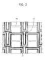
- FIG. 2 is a plan view for showing the thin film AMA
- FIG. 3 is a perspective view for showing the thin film AMA in FIG. 2
- FIG. 4 is a cross-sectional view taken along line A 1 -A 2 of FIG. 3.
- the thin film AMA has a substrate 31, an actuator 57 formed on the substrate 31, and a reflecting member 55 formed at a central portion of the actuator 57.
- the substrate 31 including electrical wiring has a connecting terminal 33 formed on the electrical wiring, a passivation layer 35 overlayed on the substrate 31 and on the connecting terminal 33, and an etching stop layer 37 overlayed on the passivation layer 35.
- the actuator 57 has a supporting layer 43, a bottom electrode 45, an active layer 47, a top electrode 49 and a via contact 53.
- the supporting layer 43 has a first portion attached beneath the bottom electrode 45 and a second portion exposed out of the bottom electrode 45. Bottoms of both lateral borders of the supporting layer 43 are partially attached to the etching stop layer 37.
- the attached portions of the supporting layer 43 are called anchors 43a, 43b which support the actuator 57.
- the lateral borders of the supporting layer 43 are parallelly prolonged from the attached portions.
- the central portion of the supporting layer 43 is integrally formed with the lateral borders between the lateral borders.
- the central portion of the supporting layer 43 has a rectangular shape.
- the bottom electrode 45 is formed on the central portion and on the lateral borders of the supporting layer 43.
- the active layer 47 is formed on the bottom electrode 45 and the top electrode 49 is formed on the active layer 47.
- the bottom electrode 45 has a U shape.
- the active layer 47 is smaller than the bottom electrode 45 and has the same shape as that of the bottom electrode 45.
- the top electrode 49 is smaller than the active layer 47 and has the same shape as that of the active layer 47.
- the via contact 53 is formed in a via hole 51 which is formed from a portion of the active layer 47 to the connecting terminal 33 through the bottom electrode 45, the supporting layer 43, the etching stop layer 37 and the passivation layer 35.
- the via contact 53 connects the bottom electrode 45 to the connecting terminal 33.
- the reflecting member 55 for reflecting an incident light is formed at the central portion of the supporting layer 43.
- the reflecting member 55 has a predetermined thickness from the surface of the supporting layer 43 to a side of the active layer 47.
- the reflecting member 55 is a mirror which has a rectangular shape.
- a method for manufacturing the thin film AMA will be described as follows.
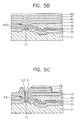
- FIGs. 5A to 5D illustrate manufacturing steps of the thin film AMA.
- the passivation layer 35 is formed on the substrate 31 having the electrical wiring (not shown) and the connecting terminal 33.
- the electrical wiring and the connecting terminal 33 receive the first signal (picture signal) from outside and transmit the first signal to the bottom electrode 45.
- the electrical wiring has a metal oxide semiconductor (MOS) transistor for switching operation.
- MOS metal oxide semiconductor
- the connecting terminal 33 is formed by using a metal, for example tungsten (W).
- the connecting terminal 33 is connected to the electrical wiring.
- the passivation layer 35 is formed by using phosphor-silicate glass (PSG) and by chemical vapor deposition (CVD) method so that the passivation layer 35 has a thickness of between 0.1 ⁇ m and 1.0 ⁇ m.
- the passivation layer 35 protects the substrate 31 having the electrical wiring and the connecting terminal 33 during subsequent manufacturing steps.
- the etching stop layer 37 is formed on the passivation layer 35 by using a nitride and by low pressure chemical vapor deposition (LPCVD) method so that the etching stop layer 37 has a thickness of between 1000 ⁇ and 2000 ⁇ .
- LPCVD low pressure chemical vapor deposition
- a sacrificial layer 39 is formed on the etching stop layer 37 by using a PSG and by atmospheric pressure CVD (APCVD) method so that the sacrificial layer 39 has a thickness of between 0.5 ⁇ m and 4.0 ⁇ m.
- APCVD atmospheric pressure CVD
- the degree of flatness of the sacrificial layer 39 is poor because the sacrificial layer 39 covers the top of the substrate 31 including the electrical wiring and the connecting terminal 33. Therefore, the surface of the sacrificial layer 39 is planarized by using a spin on glass (SOG) or by chemical mechanical polishing (CMP) method.
- SOG spin on glass
- CMP chemical mechanical polishing
- a first portion of the sacrificial layer 39 having the connecting terminal 33 thereunder and a second portion of the sacrificial layer 39 which is adjacent to the first portion of the sacrificial layer 39 are etched in order to expose a first portion of the etching stop layer 37 having the connecting terminal 33 thereunder and a second portion of the etching stop layer 37 which is adjacent to the first portion of the etching layer 37 with respect to form the supporting layer 43.
- a first layer is formed on the first and second portions of the etching stop layer 37 and on the sacrificial layer 39.
- the first layer is formed by using a rigid material such as a nitride or a metal.
- the first layer is formed by LPCVD method so that the first layer has a thickness of between 0.1 ⁇ m and 1.0 ⁇ m.
- the first layer will be patterned so as to form the supporting layer 43.
- a bottom electrode layer is formed on the first layer by using an electrically conductive metal such as platinum (Pt), tantalum (Ta) or platinum-tantalum (Pt-Ta).
- the bottom electrode layer is formed by sputtering method or CVD method so that the bottom electrode layer has a thickness of between 0.1 ⁇ m and 1.0 ⁇ m. Subsequently, the bottom electrode layer is iso-cutted in order to separate each bottom electrode layer, so each pixel of the thin film AMA independently receives the first signal from outside through the electrical wiring and the connecting terminal 33.
- the bottom electrode layer will be patterned to form the bottom electrode 45.
- a second layer is formed on the bottom electrode layer by using a piezoelectric material such as PZT (Pb(Zr, Ti)O 3 ) or PLZT ((Pb, La)(Zr, Ti)O 3 ) so that the second layer has a thickness of between 0.1 ⁇ m and 1.0 ⁇ m. Preferably, the second layer has a thickness of about 0.4 ⁇ m.
- the second layer is formed by sol-gel method, sputtering method or CVD method, the second layer is annealed by rapid thermal annealing (RTA) method. The second layer will be patterned to form the active layer 47.
- RTA rapid thermal annealing
- a top electrode layer is formed on the second layer by using an electrically conductive metal, for example, aluminum (A1), platinum or silver (Ag).
- the top electrode layer is formed by sputtering method or CVD method so that the top electrode layer has a thickness of between 0.1 ⁇ m and 1.0 ⁇ m.
- the top electrode layer also will be patterned to form the top electrode 49.
- the top electrode layer is patterned to form the top electrode 49 by using the first photo resist as an etching mask. As a result, the top electrode 49 has a U shape.
- the second signal bias signal is applied to the top electrode 49 for generating the electric field between the top electrode 49 and the bottom electrode 45.
- a second photo resist (not shown) is coated on the top electrode 49 and on the second layer by spin coating method after the first photo resist is removed by etching.
- the second layer is patterned to form the active layer 47 by using the second photo resist as an etching mask.
- the active layer 47 has a U-shape which is wider than that of the top electrode 49.
- a third photo resist (not shown) is coated on the top electrode 49, on the active layer 47 and on the bottom electrode layer by spin coating method.
- the bottom electrode layer is patterned to form the bottom electrode 45 by using the third photo resist as an etching mask.
- the bottom electrode 45 has a U-shape which is wider than that of the active layer 47.
- the third photo resist is removed by etching.
- the via contact 53 is formed in the via hole 51 by using an electrically conductive metal such as tungsten (W), platinum, aluminum or titanium.
- the via contact 53 is formed by sputtering method or CVD method so that the via contact 53 is formed from the connecting terminal 33 to the bottom electrode 45.
- the via contact 53 connects the bottom electrode 45 to the connecting terminal 33.
- the first layer is patterned to form the supporting layer 43 by using a fourth photo resist (not shown) as an etching mask after the fourth photo resist is coated on the bottom electrode 45 by spin coating method.
- the supporting layer 43 has the lateral borders and the central portion. The bottoms of the lateral borders of the supporting layer 43 are partially attached to the etching stop layer 37 and are called anchors 43a, 43b. The lateral borders of the supporting layer 43 are formed parallel to and above the etching stop layer 37 from the attached portions.
- the central portion of the supporting layer 43 is integrally formed with the lateral borders between the lateral borders.
- the central portion of the supporting layer 43 has a rectangular shape. Then, the fourth photo resist is removed by etching. A portion of sacrificial layer 39 is exposed when the first layer is patterned.
- the reflecting member 55 is formed on the central portion of the supporting layer 43 by using a reflective material such as silver, platinum, or aluminum.
- the reflecting member 55 is formed by sputtering method or CVD method so that the reflecting member 55 has a thickness of between 0.3 ⁇ m and 2.0 ⁇ m.
- the reflecting member 55 for reflecting the incident light from a light source (not shown) has the same shape as that of the central portion of the supporting layer 43.
- the fifth photo resist and the sacrificial layer 39 are removed by using hydrogen fluoride (HF) vapor, so the actuator 57 is complete.
- HF hydrogen fluoride
- the first signal is applied to the bottom electrode 45 from outside through the electrical wiring, the connecting terminal 33 and the via contact 53.
- the second signal is applied to the top electrode 49 from a common line (not shown)
- the electric field is generated between the top electrode 49 and the bottom electrode 45.
- the active layer 47 formed between the top electrode 49 and the bottom electrode 45 is deformed by the electric field.
- the active layer 47 is deformed in the direction perpendicular to the electric field.
- the actuator 57 having the active layer 47 is actuated in the opponent direction to the position where the supporting layer 43 is positioned. That is, the actuator 57 is actuated upward and the supporting layer 43 attached to bottom electrode 45 is also actuated upward according to the tilting of the actuator 57.
- the reflecting member 55 reflecting the incident light from the light source is tilted with the actuator 57 because the reflecting member 55 is formed at the central portion of the supporting layer 43. Hence, the reflecting member 55 reflects the light onto a screen so the picture is formed on the screen.
- the actuator may be initially tilted without applying of the first and the second signals because the deformation driving force such as uneven residual stresses and stress gradient are applied to the stress concentration line which is generated when the sacrificial layer is patterned so as to form the anchors for supporting the actuator. Therefore, the light efficiency of the incident light may be decrease because the reflecting member does not have a desired tilting angle when the actuator is initially tilted, so the quality of the picture projected onto the screen is decreased.
- a thin film actuated mirror array in an optical projection system having an active matrix, a supporting member, a first actuating part, a second actuating part and a reflecting member.
- the active matrix has a substrate including a metal oxide semiconductor transistor installed therein for switching operation and a first metal layer having a drain pad prolonged from a drain of the metal oxide semiconductor for transmitting a first signal.
- the supporting member has a supporting line, a supporting layer, a first anchor and two second anchors.
- the supporting line is formed above the active matrix and the supporting layer is integrally formed with the supporting line.
- the supporting layer has a rectangular ring shape.
- the first anchor and the second anchors are respectively formed between the active matrix and portions of the supporting layer adjacent to the supporting line.
- the first actuating part has a first bottom electrode, a first active layer and a first top electrode.
- the first bottom electrode receives the first signal.
- the first bottom electrode is formed at a first portion of the supporting layer which is formed perpendicular to the supporting line and the first top electrode corresponds to the first bottom electrode.
- the first top electrode receives a second signal and generates a first electric field.
- the first active layer is formed between the first bottom electrode and the first top electrode and is deformed by the first electric field.
- the second actuating part also has a second bottom electrode, a second active layer and a second top electrode.
- the second bottom electrode receives the first signal.
- the second bottom electrode is formed at a second portion of the supporting layer which is formed perpendicular to the supporting line.
- the second top electrode corresponds to the second bottom electrode and receives the second signal so it generates a second electric field.
- the second active layer is formed between the second bottom electrode and the second top electrode and deformed by the second electric field.
- the reflecting member is formed above the first actuating part and the second actuating part so as to reflect an incident light.
- the active matrix further has a first passivation layer formed on the first metal layer and on the substrate, a second metal layer formed on the first passivation layer, a second passivation layer formed on the second metal layer and an etching stop layer formed on the second passivation layer.
- the first bottom electrode has a rectangular shape having a protruding portion
- the first active layer has a rectangular shape smaller than the first bottom electrode
- the first top electrode has a rectangular shape smaller than the first active layer.
- the second bottom electrode has a rectangular shape having a protruding portion corresponding to the protruding portion of the first bottom electrode
- the second active layer has a rectangular shape smaller than the second bottom electrode
- the second top electrode has a rectangular shape smaller than the second active layer.
- the first bottom electrode has an inversed L shape and the second bottom electrode has an L shape corresponding to the first bottom electrode.
- the first anchor is formed beneath and between the first actuating part and the second actuating part and is attached to a first portion of the active matrix where the drain pad is formed thereunder, and the second anchors are respectively formed beneath outsides of the first actuating part and the second actuating part.
- the second anchors are respectively attached to a second portion and to a third portion of the active matrix which are adjacent to the first portion of the active matrix.
- the thin film actuated mirror array further has a via contact for transmitting the first signal from the drain pad to the first bottom electrode and to the second bottom electrode, a first bottom electrode connecting member formed from the via contact to the protruding portion of the first bottom electrode and a second bottom electrode connecting member formed from the via contact to the protruding portion of the second bottom electrode.
- the via contact is formed in a via hole which is formed from the first anchor to the drain pad.
- the via contact, the first bottom electrode connecting member and the second bottom electrode connecting member are formed by using an electrically conductive metal such as silver, platinum, tantalum or platinum-tantalum.
- the thin film actuated mirror array further has a common line for transmitting the second signal, a first insulating member formed from a portion of the first top electrode to a portion of the supporting layer via a portion of the first bottom electrode, a first top electrode connecting member formed from the common line to the first top electrode via the first insulating member, a second insulating member formed from a portion of the second top electrode to a portion of the supporting layer via a portion of the second bottom electrode, and a second top electrode connecting member formed from the common line to the second top electrode via the second insulating member.
- the common line is formed on the supporting line.
- the first and the second insulating members are formed by using amorphous silicon or low temperature oxide such as silicon dioxide (SiO 2 ) or phosphorus pentoxide (P 2 O 5 ).
- the first and the second, top electrode connecting members are formed by using an electrically conductive metal such as silver, platinum, tantalum or platinum-tantalum.
- a post for supporting the reflecting member is formed between a central portion of the reflecting member and a portion of the supporting layer which is apart parallel to the supporting line.
- the first signal is applied from outside to the first and the second bottom electrodes via the MOS transistor installed in the substrate, the drain pad of the first metal layer, the via contact, and the first and the second bottom electrode connecting members.
- the second signal is applied from outside to the first and the second top electrodes via the common line and the first and the second top electrode connecting members.
- the first electric field is generated between the first top electrode and the first bottom electrode
- the second electric field is generated between the second top electrode and the second bottom electrode.
- the first active layer formed between the first top electrode and the first bottom electrode is deformed by the first electric field
- the second active layer formed between the second top electrode and the second bottom electrode is deformed by the second electric field.
- the first and the second active layers are respectively deformed in the directions perpendicular to the first and the second electric fields.
- the first actuating part having the first active layer and the second actuating part having the second active layer are actuated in the opponent direction to the position where the supporting layer is located. That is, the first and the second actuating parts are actuated upward and the supporting layer attached to the first and the second bottom electrodes is also actuated upward according to the tiltings of the first and the second actuating parts.
- the reflecting member is supported by the post which is formed on the portion of the supporting layer.
- the reflecting member reflecting the incident light from the light source is tilted with the first and the second actuating parts. Hence, the reflecting member reflects the light onto a screen, so a picture is formed on the screen.
- the first and the second anchors supporting the actuating parts are formed in perpendicular direction to the actuating parts.
- the actuating parts have level surfaces without initial tiltings because the stress concentration line is not generated between the anchors and the actuating parts.
- the desired reflection angle of the reflecting member formed on the actuating parts may be regular, so the light efficiency is enhanced and the quality of the picture projected onto the screen is increased.
- the electrical shorts generated between the top electrodes and the bottom electrodes are prevented by the insulating members. Therefore, point defects of pixels in the thin film AMA are effectively decreased.
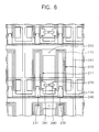
- FIG. 6 is a plan view for showing a thin film actuated mirror array in an optical projection system according to the present invention
- FIG. 7 is a perspective view for showing the thin film actuated mirror array in FIG. 6
- FIG. 8 is a cross-sectional view taken along line B 1 -B 2 of FIG. 7
- FIG. 9 is a cross-sectional view taken along line C 1 -C 2 of FIG. 7.
- the thin film AMA has an active matrix 100, a supporting member 175 formed on the active matrix 100, a first actuating part 210 and a second actuating part 211 respectively formed on the supporting member 175, and a reflecting member 260 formed above the first actuating part 210 and above the second actuating part 211.
- the active matrix 100 has a substrate 101 including M x N (M, N are integers) numbers of P-MOS transistors 120, a first metal layer 135 prolonged from a source 110 and from a drain 105 of the P-MOS transistor 120, a first passivation layer 140, a second metal layer 145, a second passivation layer 150, and an etching stop layer 155.
- the first metal layer 135 is formed on the substrate 101 and the first passivation layer 140 is formed on the first metal layer 135 and on the substrate 101.
- the second metal layer 145 is formed on the first passivation layer 140 and the second passivation layer 150 is formed on the second metal layer 145.
- the etching stop layer 155 is formed on the second passivation layer 150.
- the first metal layer 135 has a drain pad prolonged from the drain 105 of the P-MOS transistor 120 to a first anchor 171 which is formed beneath and between the first actuating part 210 and the second actuating part 211.
- the second metal layer 145 includes a titanium layer and a titanium nitride layer. A hole 147 is formed at a portion of the second metal layer 145 having the drain pad of the first metal layer 135 formed thereunder.
- the supporting member 175 has a supporting line 174, a supporting layer 170, the first anchor 171 and two second anchors 172a, 172b.
- the supporting line 174 and the supporting layer 170 are formed above the etching stop layer 155.
- a first air gap 165 is interposed between the etching stop layer 155 and the supporting line 174.
- the first air gap 165 is also interposed between the etching stop layer 155 and the supporting layer 170.
- a common line 240 is formed on the supporting line 174.
- the supporting line 174 plays a role of supporting the common line 240.
- the supporting layer 170 has a rectangular ring shape.
- the supporting layer 170 is integrally formed with the supporting line 174.
- the first anchor 171 is formed beneath and between two arms of the rectangular ring-shaped supporting layer 170. These two arms of the supporting layer 170 are perpendicularly prolonged from the supporting line 174.
- the first anchor 171 is attached to a first portion of the etching stop layer 155 having the drain pad of the first metal layer 135 formed thereunder.
- the first anchor 171 is integrally formed with those two arms of the supporting layer 170.
- the two second anchors 172a, 172b are respectively formed beneath outsides of those two arms of the supporting layer 170.
- the second anchors 172a, 172b are also integrally formed with those two arms of the supporting layer 170.
- the second anchors 172a, 172b are respectively attached to a second portion of the etching stop layer 155 and to a third portion of the etching stop layer 155.
- the first anchor 171 and the two second anchors 172a, 172b are attached beneath portions of the supporting layer 170 which are adjacent to the supporting line 174.
- the first anchor 171 and the second anchors 172a, 172b together support the supporting layer 170, so the first anchor 171 and the second anchors 172a, 172b support the first actuating part 210 and the second actuating part 211.
- the first anchor 171 and the second anchors 172a, 172b respectively have box-shapes.
- a central portion of the supporting layer 170 is supported by the first anchor 171 and lateral portions of the supporting layer 170 are supported by the second anchors 172a, 172b. Therefore, a vertical section of the supporting member 175 has a T shape as shown in FIG. 8.
- a via hole 270 is formed from the surface of a central portion of the first anchor 171 to the drain pad of the first metal layer 135 through portions of the etching stop layer 155, the second passivation layer 150, the hole 147 of the second metal layer 145 and the first passivation layer 140.
- a via contact 280 is formed in the via hole 270.
- the first actuating part 210 and the second actuating part 211 are respectively formed on those two arms of the supporting layer 170.
- the first actuating part 210 and the second actuating part 211 are formed parallel to each other.
- the first actuating part 210 has a first bottom electrode 180, a first active layer 190 and a first top electrode 200.
- the second actuating part 211 has a second bottom electrode 181, a second active layer 191 and a second top electrode 201.
- the first bottom electrode 180 is formed on one of those two arms of the supporting layer 170.
- the first bottom electrode 180 has a rectangular shape including a protruding portion, preferably, the first bottom electrode 180 has an inversed L shape.
- the first bottom electrode 180 is apart from the supporting line 174 by a predetermined interval.
- the protruding portion of the first bottom electrode 180 is prolonged downward like a stair.
- the protruding portion of the first bottom electrode 180 is prolonged to a portion of the first anchor 171 adjacent to the via hole 270.
- the first active layer 190 is formed on the first bottom electrode 180.
- the first active layer 190 has a rectangular shape which is smaller than the first bottom electrode 180.
- the first top electrode 200 is formed on the first active layer 190.
- the first top electrode 200 has a rectangular shape which is smaller than the first active layer 190.
- the second bottom electrode 181 is formed on the other of the two arms of the supporting layer 170.
- the second bottom electrode 181 has a rectangular shape having a protruding portion, preferably, the second bottom electrode 181 has an L shape which is corresponding to the first bottom electrode 180.
- the second bottom electrode 181 is also apart from the supporting line 174 by a predetermined interval.
- the protruding portion of the second bottom electrode 181 is prolonged to a portion of the first anchor 171 adjacent to the via hole 270 like the protruding portion of the first bottom electrode 180. Hence, these protruding portions of the first and the second bottom electrodes 180, 181 are correspondingly formed centering around the via hole 270.
- the second active layer 191 is formed on the second bottom electrode 181.
- the second active layer 191 has a rectangular shape which is smaller than the second bottom electrode 181.
- the second top electrode 201 is formed on the second active layer 191.
- the second top electrode 201 has a rectangular shape which is smaller than the second active layer
- the via contact 280 is formed from the drain pad of the first metal layer 135 to the top of the via hole 270.
- a first bottom electrode connecting member 290 is formed from the via contact 280 to the protruding portion of the first bottom electrode 180.
- the first bottom electrode 180 is connected to the drain pad of the first metal layer 135 through the via contact 280 and the first bottom electrode connecting member 290.
- a second bottom electrode connecting member 291 is formed from the via contact 280 to the protruding portion of the second bottom electrode 181.
- the second bottom electrode 181 is connected to the drain pad of the first metal layer 135 through the via contact 280 and the second bottom electrode connecting member 291.
- a first insulating member 220 is formed from a portion of the first top electrode 200 to a portion of the supporting layer 170 which is adjacent the supporting line 174.
- a first top electrode connecting member 230 is formed a portion of the first top electrode 200 to the common line 240 via the first insulating member 220.
- the first top electrode connecting member 230 connects the first top electrode 200 to the common line 240.
- the first insulating member 220 prevents the first top electrode 200 from connecting to the first bottom electrode 180, so the first insulating member 220 prevents an electrical short from generating between the first top electrode 200 and the first bottom electrode 180.
- a second insulating member 221 is formed from a portion of the second top electrode 201 to a portion of the supporting layer 170 which is adjacent the supporting line 174.
- a second top electrode connecting member 231 is formed a portion of the second top electrode 201 to the common line 240 via the second insulating member 221.
- the second top electrode connecting member 231 connects the second top electrode 201 to the common line 240.
- the second insulating member 221 and the second top electrode connecting member 231 are respectively formed parallel to the first insulating layer 220 and the first top electrode connecting member 230.
- the second insulating member 221 prevents the second top electrode 201 from connecting to the second bottom electrode 181, so the second insulating member 221 prevents an electrical short from generating between the second top electrode 201 and the second bottom electrode 181.
- the post 250 is formed at a portion of the supporting layer 170 having the rectangular ring shape at which the first actuating part 210 and the second actuating part 211 aren't formed (That is, a portion of the supporting layer 170 is apart in parallel direction to the supporting line 174).
- the post 250 supports the reflecting member 260.
- the reflecting member 260 has a rectangular shape.
- the central portion of the reflecting member 260 is supported by the post 250.
- the lateral portions of the reflecting member 260 are parallely formed above the first actuating part 210 and above the second actuating part 211.
- a second air gap 310 is interposed between those lateral portions of the reflecting member 260 and the first and the second actuating parts 210, 211.
- the reflecting member 260 is tilted according as the first actuating part 210 and the second actuating part 211 are actuated, so the reflecting member 260 reflects the incident light from a light source (not shown) by a predetermined angle.
- a method for manufacturing the thin film AMA in an optical projection system according to the present invention will be described as follows.
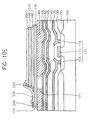
- FIGs. 10A to 10G illustrate manufacturing steps of the thin film AMA according to the present invention.
- the same reference numerals are used for the same elements in FIG. 7.
- an isolating layer 125 is formed on the substrate 101 in order to separate an active region and a field region in the substrate 101 by local oxidation of silicon method after the substrate 101 composed of silicon is provided.
- the substrate 101 is an N-typed silicon wafer.
- M x N (M, N are integers) numbers of P-typed metal oxide semiconductor (MOS) transistors 120 are completed according as the P + source 110 and the P + drain 105 are formed on the active region after a gate 115 is formed between the source 110 and the drain 105.
- the P-MOS transistor 120 receives a first signal (picture signal) from outside and performs a switching operation.
- the layer 130 is patterned to form the first metal layer 135.
- the first metal layer 135 has a drain pad prolonged from the drain 105 of the P-MOS transistor 120 to the first anchor 171 which supports the supporting layer 170.
- the first passivation layer 140 is formed on the first metal layer 135 and on the substrate 101.
- the first passivation layer 140 is formed by using phosphor-silicate glass (PSG).
- the first passivation layer 140 is formed by chemical vapor deposition (CVD) method so that the first passivation layer 140 has a thickness of between about 8000 ⁇ and 9000 ⁇ .
- the first passivation layer 140 protects the substrate 101 having the P-MOS transistor 120 during subsequent manufacturing steps.
- the second metal layer 145 is formed on the first passivation layer 140.
- the second metal layer 145 is composed of the titanium layer and the titanium nitride layer.
- the titanium layer is formed on the first passivation layer 140 by sputtering method so that the titanium layer has a thickness of between about 300 ⁇ and 500 ⁇ .
- the titanium nitride layer is formed on the titanium layer by physical vapor deposition (PVD) method so that the titanium nitride layer has a thickness of between about 1000 ⁇ and 1200 ⁇ .
- PVD physical vapor deposition
- the second metal layer 145 excludes the light incident upon the substrate 101, so the second metal layer 145 prevents a photo leakage current from flowing through the substrate 101.
- a portion of the second metal layer 145 having the drain pad formed thereunder is etched so as to form the hole 147.
- the hole 147 isolates the via contact 280 from the second metal layer 145.
- the second passivation layer 150 is formed on the second metal layer 145 and on the hole 147.
- the second passivation layer 150 is formed by using phosphor-silicate glass.
- the second passivation layer 150 is formed by CVD method so that the second passivation layer 150 has a thickness of between about 2000 ⁇ and 3000 ⁇ .
- the second passivation layer 150 protects the second metal layer 145 and the resultant layers formed on the substrate 101 during subsequent manufacturing steps.
- the etching stop layer 155 is formed on the second passivation layer 150 by using low temperature oxide (LTO) such as silicon dioxide (SiO 2 ) or phosphorus pentoxide (P 2 O 5 ).
- LTO low temperature oxide
- the etching stop layer 155 is formed by low pressure CVD (LPCVD) method under a temperature of between about 350°C and 450°C so that the etching stop layer 155 has a thickness of between about 0.2 ⁇ m and 0.8 ⁇ m.
- LPCVD low pressure CVD
- the etching stop layer 155 protects the second passivation layer 150 and the resultant layers formed on the substrate 101 during subsequent etching steps.
- the active matrix 100 is completed, which is composed of the substrate 101, the first metal layer 135, the first passivation layer 140, the second metal layer 145, the second passivation layer 150 and the etching stop layer 155.
- a first sacrificial layer 160 is formed on the etching stop layer 155 by using poly silicon below a temperature of about 500°C.
- the first sacrificial layer 160 is formed by LPCVD method so that the first sacrificial layer 160 has a thickness of between about 2.0 ⁇ m and 3.0 ⁇ m.
- the degree of flatness of the first sacrificial layer 160 is poor because the first sacrificial layer 160 covers the top of the active matrix 100 having the MOS transistor 120 and the resultant layers. Therefore, the surface of the first sacrificial layer 160 is planarized by using spin on glass (SOG) or by chemical mechanical polishing (CMP) method so that the first sacrificial layer 160 has a thickness of about 1.1 ⁇ m.
- SOG spin on glass
- CMP chemical mechanical polishing
- FIG. 10B illustrates a plan view for showing the patterned first sacrificial layer 160.
- a first photo resist (not shown) is coated on the first sacrificial layer 160 and is patterned, a first portion of the first sacrificial layer 160 having the hole 147 of the second metal layer 145 formed thereunder and a second and a third portions of the first sacrificial layer 160 adjacent to the first portion are etched to expose portions of the etching stop layer 155.
- the first anchor 171 and the second anchors 172a, 172b will be formed at the exposed portions of the etching stop layer 155. These exposed portions of the etching stop layer 155 respectively have rectangular shapes which are separated by predetermined intervals. Then, the first photo resist is removed.
- a first layer 169 is formed on those exposed portions of the etching stop layer 155 which have rectangular shapes and on the first sacrificial layer 160.
- the first layer 169 is formed by using a rigid material such as nitride or metal.
- the first layer 169 is formed by LPCVD method so that the first layer 169 has a thickness of between about 0.1 ⁇ m and 1.0 ⁇ m.
- the first layer 169 will be patterned so as to form the supporting member 175 having the supporting layer 170, the supporting line 174, the first anchor 171 and the two second anchors 172a, 172b.
- the first anchor 171 locates at the center of the exposed portions of the etching stop layer 155 and the two second anchors 172a, 172b respectively locate at other exposed portions of the etching stop layer 155.
- a bottom electrode layer 179 is formed on the first layer 169.
- the bottom electrode layer 179 is formed by using electrically conductive metal such as platinum (Pt), tantalum (Ta) or platinum-tantalum (Pt-Ta).
- the bottom electrode layer 179 is formed by sputtering method or CVD method so that the bottom electrode layer 179 has a thickness of between about 0.1 ⁇ m and 1.0 ⁇ m.
- the bottom electrode layer 179 will be patterned to form the first bottom electrode 180 and the second bottom electrode 181 respectively having the protruding portions which are opposed to each other.
- a second layer 189 is formed on the bottom electrode layer 179.
- the second layer 189 is formed by using piezoelectric material such as PZT (Pb(Zr, Ti)O 3 ) or PLZT ((Pb, La)(Zr, Ti)O 3 ) and by sol-gel method, sputtering method or CVD method so that the second layer 189 has a thickness of between about 0.1 ⁇ m and 1.0 ⁇ m.
- the second layer 189 is formed by the sputtering method and by using the PZT produced according to the sol-gel method so that the second layer 189 has a thickness of about 0.4 ⁇ m.
- the second layer 189 is annealed by rapid thermal annealing (RTA) method.
- the second layer 189 will be patterned to form the first active layer 190 and the second active layer 191 which are respectively deformed by the first electric field and the second electric field.
- a top electrode layer 199 is formed on the second layer 189.
- the top electrode layer 199 is formed by using an electrically conductive metal, for example, tantalum, platinum or silver (Ag).
- the top electrode layer 199 is formed by sputtering method or CVD method so that the top electrode layer 199 has a thickness of between about 0.1 ⁇ m and 1.0 ⁇ m.
- the top electrode layer 199 will be patterned so as to form the first top electrode 200 and the second top electrode 201 which are separated by a predetermined interval.
- the top electrode layer 199 is patterned so as to form the first top electrode 200 and the second top electrode 201 which are respectively have rectangular shapes (see FIG. 7) by using the second photo resist as an etching mask.
- the first top electrode 200 and the second top electrode 201 are formed parallel to each other.
- a second signal (a bias signal) is applied to the first top electrode 200 and to the second top electrode 201 through the common line 240. Then, the second photo resist is removed.
- the second layer 189 is patterned to form the first active layer 190 and the second active layer 191 by the same process of the top electrode layer 199.
- the first active layer 190 and the second active layer 191 are also formed parallel to each other.
- the first active layer 190 and the second active layer 191 respectively have rectangular shapes which are wider than the first top electrode 200 and the second top electrode 201 as shown in FIG. 7.
- the bottom electrode layer 179 is patterned to form the first bottom electrode 180 and the second bottom electrode 181 by the same method of the top electrode layer 199.
- the first bottom electrode 180 and the second bottom electrode 181 respectively have the rectangular shapes which correspondingly have the protruding portions.
- the first bottom electrode 180 has the inversed L shape and the second bottom electrode 181 has the L shape which is corresponded to the first bottom electrode 180.
- the first bottom electrode 180 and the second bottom electrode 181 are respectively wider than the first active layer 190 and the second active layer 191.
- the common line 240 is simultaneously formed at a portion of the first layer 169 which will be patterned to form the supporting line 174.
- the common line 240 is formed in the direction perpendicular to the first bottom electrode 180 and the second bottom electrode 181 as shown in FIG. 7.
- the common line 240 is separated from the first and the second bottom electrodes 180, 181 by a predetermined interval, so the common line 240 not to contact with the first bottom electrode 180 and with the second bottom electrode 181.
- the first actuating part 210 and the second actuating part 211 are completed.
- the first actuating part 210 has the first bottom electrode 180.
- the second actuating part 211 has the second bottom electrode 181, the second active layer 191 and the second top electrode 201.
- the first layer 169 is patterned to form the supporting member 175 having the supporting layer 170, the supporting line 174, the first anchor 171 and the two second anchors 172a, 172b.
- the first anchor 171 locates on the center of the exposed portion of the etching stop layer 155 and the two second anchors 172a, 172b respectively locate on the others of the exposed portions of the etching stop layer 155.
- the hole 147 of the second metal layer 145 is formed under the first anchor 171.
- the supporting layer 170 has the rectangular ring shape and is integrally formed with the supporting line 174 which is formed above the etching stop layer 155.
- the supporting member 175 is completed as shown in FIG.7 when the first sacrificial layer 160 is removed.
- the first anchor 171 is formed beneath and between the two arms of the rectangular ring-shaped supporting layer 170.
- the two arms of the supporting layer 170 are perpendicularly prolonged from the supporting line 174.
- the first anchor 171 is attached to the center of the exposed portion of the etching stop layer 155, that is a first exposed portion of the etching stop layer 155, having the drain pad of the first metal layer 135 formed thereunder.
- the first anchor 171 is integrally formed with the two arms of the supporting layer 170.
- the two second anchors 172a, 172b are respectively formed beneath outsides of the two arms of the supporting layer 170.
- the second anchors 172a, 172b are also integrally formed with the two arms of the supporting layer 170 and are respectively attached to a second and a third exposed portions of the etching stop layer 155.
- the first anchor 171 and the second anchors 172a, 172b are attached beneath the portions of the supporting layer 170 adjacent to the supporting line 174.
- the first actuating part 210 and the second actuating part 211 are respectively formed on the two arms of the supporting layer 170.
- the first anchor 171 is formed beneath and between the first actuating part 210 and the second actuating part 211 and the second anchors 172a, 172b are respectively formed beneath outsides of the first and the second actuating parts 210, 211.
- the first anchor 171 and the second anchors 172a, 172b together support the supporting layer 170, so the first anchor 171 and the second anchors 172a, 172b respectively support the first actuating part 210 and the second actuating part 211.
- the third photo resist (not shown) is coated on the supporting member 175, on the first actuating part 210 and on the second actuating part 211, the third photo resist is patterned to expose portions of the common line 240, the supporting member 175, the first top electrode 200 and the second top electrode 201. At that time, the protruding portions of the first bottom electrode 180 and the second bottom electrode 181 are simultaneously exposed.
- the first insulating member 220 and the second insulating member 221 are formed by patterning LTO such as silicon dioxide (SiO 2 ) or phosphorus pentoxide (P 2 O 5 ), after the LTO is formed on the exposed portions of the supporting member 175, the first top electrode 200 and the second top electrode 201 by LPCVD method.
- the first insulating member 220 is formed from a portion of the first top electrode 200 to a portion of the supporting layer 170 via portions of the first active layer 190 and the first bottom electrode 180.
- the second insulating member 221 is also formed from a portion of the second top electrode 200 to a portion of the supporting layer 170 via portions of the second active layer 190 and the second bottom electrode 180.
- the first insulating member 220 and the second insulating member 221 respectively have thicknesses of between about 0.2 ⁇ m and 0.4 ⁇ m, preferably, 0.3 ⁇ m.
- FIG. 10F illustrates a cross-sectional view for showing the via contact 280.
- the via hole 270 is formed from the first anchor 171 to the drain pad of the first metal layer 135 through the hole 147 of the second metal layer 145 by etching portions of the etching stop layer 155, the second passivation layer 150 and the first passivation layer 140.
- the via contact 280 is formed in the via hole 270.
- the first bottom electrode connecting member 290 and the second bottom electrode connecting member 291 are respectively formed form the via hole 270 to the protruding portions of the first bottom electrode 180 and the second bottom electrode 181.
- the first top electrode connecting member 230 is formed from the common line 240 to a portion of the first top electrode 200 via the first insulating member 220 and the supporting layer 170.
- the second top electrode connecting member 231 is also formed from the common line 240 to a portion of the second top electrode 201 via the second insulating member 221 and the supporting layer 170 as shown in FIG. 7.
- the first top electrode connecting member 230 and the second top electrode connecting member 231 are formed parallel to each other.
- the via contact 280, the first bottom electrode connecting member 290, the second bottom electrode connecting member 291, the first top electrode connecting member 230 and the second top electrode connecting member 231 are formed by using electrically conductive metals such as a platinum, tantalum or platinum-tantalum and by sputtering method or CVD method.
- the via contact 280, the first bottom electrode connecting member 290, the second bottom electrode connecting member 291, the first top electrode connecting member 230 and the second top electrode connecting member 231 are respectively have thicknesses of between about 0.1 ⁇ m and 0.2 ⁇ m.
- the first top electrode connecting member 230 and the second top electrode connecting member 231 respectively connect the common line 240 to the first top electrode 200 and to the second top electrode 201.
- the protruding portion of the first bottom electrode 180 is connected to the drain pad through the via contact 280 and the first bottom electrode connecting member 290.
- the protruding portion of the second bottom electrode 181 is connected to the drain pad through the via contact 280 and the second bottom electrode connecting member 291, too.
- a second sacrificial layer 300 is formed on the first actuating part 210, on the second actuating part 211 and on the supporting member 175.
- the second sacrificial layer 300 is formed by using poly silicon and by LPCVD method.
- the second sacrificial layer 300 sufficiently covers the first actuating part 210 and the second actuating part 211.
- the surface of the second sacrificial layer 300 is planarized by CMP method so as to the second sacrificial layer 300 has an even surface.
- a portion of the second sacrificial layer 300 is etched to expose a portion of the supporting layer 170 which is apart in parallel direction to the supporting line 174. Namely, the portion of the supporting layer 170 where the first actuating part 210 and the second actuating part 211 are not formed is exposed.
- the post 250 and the reflecting member 260 are simultaneously formed by patterning a metal layer having reflectively after the metal layer is formed on the exposed portion of the supporting layer 170 and on the sacrificial layer 300.
- the post 250 and the reflecting member 260 are formed by using aluminum and by sputtering method or CVD method.
- the central portion of the reflecting member 260 is supported by the post 250 and lateral portions of the reflecting member 260 are parallely formed above the first actuating part 210 and above the second actuating part 211.
- the reflecting member 260 has a rectangular shape.
- the thin film AMA shown in FIG. 7 is complete by rinsing and drying after the first sacrificial layer 160 and the second sacrificial layer 300 are removed by using bromine fluoride (BrF 3 or BrF 5 ) vapor or xenon fluoride (XeF 2 , XeF 4 or XeF 6 ) vapor.
- a second air gap 310 is formed at the position where the second sacrificial layer 300 is located and the first air gap 165 is formed at the position where the first sacrificial layer 160 is located.
- the first signal is applied from outside to the first and the second bottom electrodes 180, 181 via the MOS transistor 120 installed in the substrate 101, the drain pad of the first metal layer 135, the via contact 280, and the first and the second bottom electrode connecting members 290, 291.
- the second signal is applied from outside to the first and the second top electrodes 200, 201 via the common line 240 and the first and the second top electrode connecting members 230, 231.
- the first electric field is generated between the first top electrode 200 and the first bottom electrode 180 and the second electric field is generated between the second top electrode 201 and the second bottom electrode 181.
- the first active layer 190 formed between the first top electrode 200 and the first bottom electrode 180 is deformed by the first electric field and the second active layer 191 formed between the second top electrode 201 and the second bottom electrode 181 is deformed by the second electric field.
- the first and the second active layers 190, 191 are respectively deformed in the directions perpendicular to the first and the second electric fields.
- the first actuating part 210 having the first active layer 190 and the second actuating part 211 having the second active layer 191 are actuated in the opponent direction to the position where the supporting layer 170 is located.
- first and the second actuating parts 210, 211 are actuated upward and the supporting layer 170 attached to the first and the second bottom electrodes 180, 181 is also actuated upward according to the actuatings of the first and the second actuating parts 210, 211.
- the reflecting member 260 is supported by the post 250 which is formed on the portion of the supporting layer 170.
- the reflecting member 260 reflecting the incident light from the light source is tilted with the first and the second actuating parts 210, 211. Hence, the reflecting member 260 reflects the light onto the screen, so the picture is projected on the screen.
- the supporting member has the supporting line, the supporting layer having the rectangular ring shape, the first anchor and the second anchors.
- the first and the second actuating parts are respectively formed two arms of the rectangular ring shaped supporting layer.
- the anchors supporting the actuating parts are formed in perpendicular direction to the actuating parts.
- the actuating parts have level surfaces without initial tiltings because the stress concentration line does not generated between the anchors and the actuating parts.
- the desired reflection angle of the reflecting member formed on the actuating parts may be regular, so the light efficiency is enhanced and the quality of the picture projected onto the screen is increased.
Landscapes
- Physics & Mathematics (AREA)
- General Physics & Mathematics (AREA)
- Optics & Photonics (AREA)
- Mechanical Light Control Or Optical Switches (AREA)
Claims (15)
- Matrice de miroirs actionnés par film mince pour un système de projection optique, laquelle matrice de miroirs actionnés par film mince est actionnée par un premier signal et un second signal et comprend :une matrice active (100) possédant un substrat (101) dans lequel est installé un transistor semi-conducteur à oxyde métallique destiné aux opérations de commutation et une première couche métallique (135) comprenant un plot de drain prolongeant un drain (105) du semi-conducteur à l'oxyde métallique (120) pour transmettre le premier signal ;un moyen de support (175) possédant 1) une ligne de support formée pardessus ladite matrice active et 2) une couche de support (170) ayant une forme annulaire rectangulaire, ladite couche de support étant solidaire de ladite ligne de support, et 3) un premier ancrage et deux deuxièmes ancrages, formés respectivement entre ladite matrice active et des parties de ladite couche de support adjacentes à ladite ligne de support ;une première partie d'actionnement (210) comprenant a) une première électrode inférieure (180) destinée à recevoir le premier signal, laquelle première électrode inférieure est formée dans une première partie de ladite couche de support (170) perpendiculaire à ladite ligne de support, b) une première électrode supérieure (200) correspondant à ladite première électrode inférieure (180) et destinée à recevoir le second signal etproduisant un premier champ électrique, et c) une première couche active formée entre ladite première électrode inférieure et ladite première électrode supérieure et déformée par le premier champ électrique ;une deuxième partie d'actionnement (211) comprenant i) une deuxième électrode inférieure (181) destinée à recevoir le premier signal, laquelle deuxième électrode inférieure (181) est formée dans une deuxième partie de ladite couche de support perpendiculaire à ladite ligne de support, ii) une deuxième électrode supérieure correspondant à ladite deuxième électrode inférieure (181) et destinée à recevoir le second signal et à produire un second champ électrique, et iii) une seconde couche active formée entre ladite deuxième électrode inférieure (181) et ladite deuxième électrode supérieure (201) et déformée par le second champ électrique ; etun moyen réfléchissant (266) destiné à réfléchir une lumière, lequel moyen réfléchissant est formé au-dessus de ladite première partie d'actionnement (210) et de ladite deuxième partie d'actionnement (211).
- Matrice de miroirs actionnés par film mince pour un système de projection optique selon la revendication 1, laquelle matrice active (100) comprend en outre :une première couche de passivation (140) formée sur ladite première couche métallique et sur ledit substrat (101) ;une seconde couche métallique formée sur ladite première couche de passivation ;une seconde couche de passivation (150) formée sur ladite seconde couche métallique (145) ; etune couche d'arrêt de gravure (155) formée sur ladite seconde couche de passivation (150).
- Matrice de miroirs actionnés par film mince pour un système de projection optique selon la revendication 1, caractérisée en ce que ladite première électrode inférieure (180) est de forme rectangulaire avec une partie en saillie, ladite première couche active (190) est en forme de rectangle plus petit que ladite première électrode inférieure (180), ladite première électrode supérieure est en forme de rectangle plus petit que ladite première couche active (190), ladite deuxième électrode inférieure (181) est en forme de rectangle avec une partie en saillie correspondant à la partie en saillie de ladite première électrode inférieure (180), ladite seconde couche active (191) est en forme de rectangle plus petit que ladite deuxième électrode inférieure (181) et ladite 201 est en forme de rectangle plus petit que ladite seconde couche active (191).
- Matrice de miroirs actionnés par film mince pour un système de projection optique selon la revendication 3, caractérisé en ce que ladite première électrode inférieure (180) est en forme de L inversé et ladite deuxième électrode inférieure (181) a une forme en L correspondant à ladite première électrode inférieure (180).
- Matrice de miroirs actionnés par film mince pour un système de projection optique selon la revendication 3, caractérisé en ce que ledit premier ancrage (171) est formé sous et entre ladite première partie d'actionnement (210) et ladite deuxième partie d'actionnement (211) et fixé à une première partie de ladite matrice active (100) dans laquelle le plot de drain est formé, et lesdits deuxièmes ancrages sont formés respectivement à coté des faces extérieures de ladite première partie d'actionnement (210) et de ladite deuxième partie d'actionnement (211) et fixés respectivement à une deuxième partie et une troisième partie de ladite matrice active (100) adjacentes à la première partie de ladite matrice active (100).
- Matrice de miroirs actionnés par film mince pour un système de projection optique s 5, caractérisée en ce que ladite matrice de miroirs actionnés par film mince comprend en outre :un contact d'interconnexion destiné à transmettre le premier signal du plot de drain à ladite première électrode inférieure (180) et à ladite deuxième électrode inférieure (181), ledit contact d'interconnexion étant formé dans un trou d'interconnexion formé entre ledit premier ancrage (171) et le plot de drain ;un moyen de connexion de la première électrode inférieure (180) formé entre ledit contact d'interconnexion et la partie en saillie de ladite première électrode inférieure (180) ; etun moyen de connexion de la deuxième électrode inférieure (181) formé entre ledit contact d'interconnexion et la partie en saillie de ladite deuxième électrode inférieure (181).
- Matrice de miroirs actionnés par film mince pour un système de projection optique selon la revendication 6, caractérisée en ce que ledit contact d'interconnexion, ledit moyen de connexion de la première électrode inférieure (180) et ledit moyen de connexion de la deuxième électrode inférieure (181) sont formés avec un métal conducteur électrique tel que l'argent, le platine, le tantale ou un alliage de platine et de tantale.
- Matrice de miroirs actionnés par film mince pour un système de projection optique selon la revendication 1, dans laquelle ladite matrice de miroirs actionnés par film mince comprend en outre :une ligne commune destinée à la transmission du second signal, laquelle ligne commune est formée sur ladite ligne de support ;un premier moyen d'isolation formé entre une partie de ladite première électrode supérieure et une partie de ladite couche de support en passant par une partie de ladite première électrode inférieure (180) ;un moyen de connexion de la première électrode supérieure (200) formé entre ladite ligne commune et ladite première électrode supérieure (200) en passant par ladite première couche isolante ;un second moyen d'isolation formé entre une partie de ladite deuxième électrode supérieure (201) et une partie de ladite couche de support en passant par une partie de ladite deuxième électrode inférieure ; etun moyen de connexion de la deuxième électrode supérieure formé entre ladite ligne commune et ladite deuxième électrode supérieure en passant par ladite deuxième couche isolante.
- Matrice de miroirs actionnés par film mince pour un système de projection optique selon la revendication 8, caractérisée en ce que ledit premier moyen d'isolation et ledit deuxième second moyen d'isolation sont formés avec un silicium amorphe.
- Matrice de miroirs actionnés par film mince pour un système de projection optique selon la revendication 8, caractérisée en ce que ledit premier moyen d'isolation et ledit deuxième moyen d'isolation sont formés avec un oxyde à basse température.
- Matrice de miroirs actionnés par film mince pour un système de projection optique s 10, caractérisée en ce que ledit premier moyen d'isolation (220) et ledit deuxième moyen d'isolation (221) sont formés avec du dioxyde de silicium (SiO2) ou du pentoxyde de phosphore (P2O5).
- Matrice de miroirs actionnés par film mince pour un système de projection optique selon la revendication 8, caractérisée en ce que ledit moyen de connexion de la première électrode supérieure et ledit moyen de connexion de la deuxième électrode supérieure sont formés avec un métal conducteur électrique tel que l'argent, le platine, le tantale ou un alliage de platine et de tantale.
- Matrice de miroirs actionnés par film mince pour un système de projection optique selon la revendication 8, caractérisé en ce que ladite matrice de miroirs actionnés par film mince comprend en outre un montant destiné à supporter ledit moyen réfléchissant (260), ledit montant étant formé entre une partie centrale dudit moyen réfléchissant et une partie de ladite couche de support écartée parallèlement à ladite ligne de support.
- Matrice de miroirs actionnés par film mince pour un système de projection optique selon la revendication 1, dans laquelle la première partie d'actionnement possède une partie en saillie,
la deuxième partie d'actionnement possède une partie en saillie correspondant à la partie en saillie de ladite première électrode inférieure, avec une ligne commune pour la transmission du second signal, ladite ligne commune étant formée sur ladite ligne de support ;
avec un moyen de connexion de la première électrode supérieure (230) formé entre ladite ligne commune et ladite première électrode supérieure (200) ; et
avec un moyen de connexion de la deuxième électrode supérieure (231) formé entre ladite ligne commune et ladite deuxième électrode supérieure (201). - Matrice de miroirs actionnés par film mince pour un système de projection optique selon la revendication 1, dans laquelle la première partie d'actionnement possède une partie en saillie,
la deuxième partie d'actionnement (211) possède une partie en saillie correspondant à la partie en saillie de ladite première électrode inférieure (180),
avec un contact d'interconnexion pour la transmission du premier signal du plot de drain à ladite première électrode inférieure (180) et à ladite deuxième électrode inférieure (181), lequel contact d'interconnexion est formé dans un trou d'interconnexion formé entre ledit premier ancrage (171) et le plot de drain ;
avec un moyen de connexion de la première électrode inférieure formé entre ledit contact d'interconnexion et la partie en saillie de ladite première électrode inférieure (180) ;
avec un moyen de connexion de la deuxième électrode inférieure formé entre ledit contact d'interconnexion et la partie en saillie de ladite deuxième électrode inférieure (181);
avec une ligne commune pour la transmission du second signal, laquelle ligne commune est formé sur ladite ligne de support ;
avec un moyen de connexion de la première électrode supérieure formé entre ladite ligne commune et ladite première électrode supérieure (200) ; avec un moyen de connexion de la deuxième électrode supérieure formé entre ladite ligne commune et ladite deuxième électrode supérieure (201) ; et
avec un moyen réfléchissant (260) destiné à réfléchir une lumière, lequel moyen réfléchissant est formé au-dessus de ladite première partie d'actionnement et de ladite deuxième partie d'actionnement.
Applications Claiming Priority (2)
| Application Number | Priority Date | Filing Date | Title |
|---|---|---|---|
| PCT/KR1998/000053 WO1999049667A1 (fr) | 1998-03-20 | 1998-03-20 | Ensemble miroirs commandes par couches minces dans un systeme de projection optique |
| US09/050,935 US6005706A (en) | 1998-03-20 | 1998-03-31 | Thin film actuated mirror array in an optical projection system |
Publications (2)
| Publication Number | Publication Date |
|---|---|
| EP1062817A1 EP1062817A1 (fr) | 2000-12-27 |
| EP1062817B1 true EP1062817B1 (fr) | 2007-01-17 |
Family
ID=26633361
Family Applications (1)
| Application Number | Title | Priority Date | Filing Date |
|---|---|---|---|
| EP98908302A Expired - Lifetime EP1062817B1 (fr) | 1998-03-20 | 1998-03-20 | Ensemble miroirs commandes par couches minces pour un systeme de projection optique |
Country Status (3)
| Country | Link |
|---|---|
| US (1) | US6005706A (fr) |
| EP (1) | EP1062817B1 (fr) |
| WO (1) | WO1999049667A1 (fr) |
Families Citing this family (4)
| Publication number | Priority date | Publication date | Assignee | Title |
|---|---|---|---|---|
| US6960305B2 (en) * | 1999-10-26 | 2005-11-01 | Reflectivity, Inc | Methods for forming and releasing microelectromechanical structures |
| JP5608556B2 (ja) * | 2007-08-10 | 2014-10-15 | ボード・オブ・リージエンツ,ザ・ユニバーシテイ・オブ・テキサス・システム | 前方結像型光干渉断層(oct)システムおよびプローブ |
| CN102645811B (zh) * | 2011-11-23 | 2014-07-02 | 京东方科技集团股份有限公司 | 电子纸有源基板及其制造方法和电子纸显示屏 |
| CN113922781B (zh) * | 2021-10-15 | 2025-03-18 | 苏州汉天下电子有限公司 | 一种体声波谐振器以及通信器件 |
Family Cites Families (2)
| Publication number | Priority date | Publication date | Assignee | Title |
|---|---|---|---|---|
| EP0810458B1 (fr) * | 1996-05-29 | 2001-09-19 | Daewoo Electronics Co., Ltd | Matrice de miroirs commandés à couches minces et sa méthode de fabrication |
| KR980003662A (ko) * | 1996-06-28 | 1998-03-30 | 배순훈 | 큰 구동 각도를 가지는 박막형 광로 조절 장치 |
-
1998
- 1998-03-20 WO PCT/KR1998/000053 patent/WO1999049667A1/fr not_active Ceased
- 1998-03-20 EP EP98908302A patent/EP1062817B1/fr not_active Expired - Lifetime
- 1998-03-31 US US09/050,935 patent/US6005706A/en not_active Expired - Lifetime
Also Published As
| Publication number | Publication date |
|---|---|
| EP1062817A1 (fr) | 2000-12-27 |
| US6005706A (en) | 1999-12-21 |
| WO1999049667A1 (fr) | 1999-09-30 |
Similar Documents
| Publication | Publication Date | Title |
|---|---|---|
| US6204080B1 (en) | Method for manufacturing thin film actuated mirror array in an optical projection system | |
| US5920421A (en) | Thin film actuated mirror array in an optical projection system and method for manufacturing the same | |
| US5914803A (en) | Thin film actuated mirror array in an optical projection system and method for manufacturing the same | |
| US5886811A (en) | Thin film actuated mirror array in an optical projection system and method for manufacturing the same | |
| EP1062817B1 (fr) | Ensemble miroirs commandes par couches minces pour un systeme de projection optique | |
| US5815304A (en) | Thin film actuated mirror array in a optical projection system and method for manufacturing the same | |
| US5815305A (en) | Thin film actuated mirror array in an optical projection system and method for manufacturing the same | |
| US5917645A (en) | Thin film actuated mirror array in an optical projection system and method for manufacturing the same | |
| US5754330A (en) | Thin film actuated mirror array in an optical projection system and method for manufacturing the same | |
| US5877517A (en) | Thin film actuated mirror array in an optical projection system | |
| US5786928A (en) | Thin film actuated mirror array in an optical projection system and method for manufacturing the same | |
| RU2180158C2 (ru) | Тонкопленочная матрица управляемых зеркал для оптической проекционной системы и способ ее изготовления | |
| EP0954929B1 (fr) | Reseau de miroirs actionnes a film mince d'un systeme optique de projection, et son procede de fabrication | |
| EP0966842B1 (fr) | Groupement de miroirs actionnes, a couche mince, utilise dans un systeme de projection optique et son procede de fabrication | |
| KR100265951B1 (ko) | 박막형 광로 조절 장치 및 그 제조 방법 | |
| KR100251106B1 (ko) | 박막형 광로 조절장치의 제조 방법 | |
| KR100225587B1 (ko) | 박막형 광로 조절 장치 | |
| MXPA99006849A (es) | Operacion de espejos accionados de pelicula fina de un sistema de proyeccion optica y metodo para fabricarla | |
| KR19980040067A (ko) | 광효율을 향상시킬 수 있는 박막형 광로 조절 장치 | |
| KR20000044181A (ko) | 박막형 광로조절 장치의 제조 방법 | |
| GB2332750A (en) | Thin film actuated mirror array | |
| JP2002543442A (ja) | 薄膜型光路調節装置 | |
| KR19980054835A (ko) | 액츄에이터의 초기 휘어짐을 방지 할 수 있는 박막형 광로 조절장치 및 그 제조 방법 | |
| KR19980040068A (ko) | 광효율을 향상시킬 수 있는 박막형 광로 조절장치의 제조 방법 | |
| KR19980046151A (ko) | 광효율을 향상시킬 수 있는 박막형 광로 조절장치의 제조 방법 |
Legal Events
| Date | Code | Title | Description |
|---|---|---|---|
| PUAI | Public reference made under article 153(3) epc to a published international application that has entered the european phase |
Free format text: ORIGINAL CODE: 0009012 |
|
| 17P | Request for examination filed |
Effective date: 20001012 |
|
| AK | Designated contracting states |
Kind code of ref document: A1 Designated state(s): BE DE GB |
|
| RAP1 | Party data changed (applicant data changed or rights of an application transferred) |
Owner name: DAEWOO ELECTRONICS CORPORATION |
|
| GRAP | Despatch of communication of intention to grant a patent |
Free format text: ORIGINAL CODE: EPIDOSNIGR1 |
|
| RTI1 | Title (correction) |
Free format text: THIN FILM ACTUATED MIRROR ARRAY FOR AN OPTICAL PROJECTION SYSTEM |
|
| GRAS | Grant fee paid |
Free format text: ORIGINAL CODE: EPIDOSNIGR3 |
|
| GRAA | (expected) grant |
Free format text: ORIGINAL CODE: 0009210 |
|
| AK | Designated contracting states |
Kind code of ref document: B1 Designated state(s): BE DE GB |
|
| REG | Reference to a national code |
Ref country code: GB Ref legal event code: FG4D |
|
| REF | Corresponds to: |
Ref document number: 69836923 Country of ref document: DE Date of ref document: 20070308 Kind code of ref document: P |
|
| PLBE | No opposition filed within time limit |
Free format text: ORIGINAL CODE: 0009261 |
|
| STAA | Information on the status of an ep patent application or granted ep patent |
Free format text: STATUS: NO OPPOSITION FILED WITHIN TIME LIMIT |
|
| 26N | No opposition filed |
Effective date: 20071018 |
|
| PGFP | Annual fee paid to national office [announced via postgrant information from national office to epo] |
Ref country code: GB Payment date: 20090318 Year of fee payment: 12 |
|
| PGFP | Annual fee paid to national office [announced via postgrant information from national office to epo] |
Ref country code: DE Payment date: 20090313 Year of fee payment: 12 |
|
| PGFP | Annual fee paid to national office [announced via postgrant information from national office to epo] |
Ref country code: BE Payment date: 20090401 Year of fee payment: 12 |
|
| BERE | Be: lapsed |
Owner name: DAEWOO ELECTRONICS CORPORATION Effective date: 20100331 |
|
| GBPC | Gb: european patent ceased through non-payment of renewal fee |
Effective date: 20100320 |
|
| PG25 | Lapsed in a contracting state [announced via postgrant information from national office to epo] |
Ref country code: DE Free format text: LAPSE BECAUSE OF NON-PAYMENT OF DUE FEES Effective date: 20101001 Ref country code: BE Free format text: LAPSE BECAUSE OF NON-PAYMENT OF DUE FEES Effective date: 20100331 |
|
| PG25 | Lapsed in a contracting state [announced via postgrant information from national office to epo] |
Ref country code: GB Free format text: LAPSE BECAUSE OF NON-PAYMENT OF DUE FEES Effective date: 20100320 |