EP1063696B1 - Procédé d'amélioration de la qualité d'une couche déposée contenant du métal à partir d'un bain de métallisation - Google Patents
Procédé d'amélioration de la qualité d'une couche déposée contenant du métal à partir d'un bain de métallisation Download PDFInfo
- Publication number
- EP1063696B1 EP1063696B1 EP00870141A EP00870141A EP1063696B1 EP 1063696 B1 EP1063696 B1 EP 1063696B1 EP 00870141 A EP00870141 A EP 00870141A EP 00870141 A EP00870141 A EP 00870141A EP 1063696 B1 EP1063696 B1 EP 1063696B1
- Authority
- EP
- European Patent Office
- Prior art keywords
- metal
- containing layer
- layer
- plating bath
- deposited
- Prior art date
- Legal status (The legal status is an assumption and is not a legal conclusion. Google has not performed a legal analysis and makes no representation as to the accuracy of the status listed.)
- Expired - Lifetime
Links
Images
Classifications
-
- H—ELECTRICITY
- H10—SEMICONDUCTOR DEVICES; ELECTRIC SOLID-STATE DEVICES NOT OTHERWISE PROVIDED FOR
- H10P—GENERIC PROCESSES OR APPARATUS FOR THE MANUFACTURE OR TREATMENT OF DEVICES COVERED BY CLASS H10
- H10P14/00—Formation of materials, e.g. in the shape of layers or pillars
- H10P14/40—Formation of materials, e.g. in the shape of layers or pillars of conductive or resistive materials
- H10P14/46—Formation of materials, e.g. in the shape of layers or pillars of conductive or resistive materials using a liquid
- H10P14/47—Electrolytic deposition, i.e. electroplating; Electroless plating
-
- H—ELECTRICITY
- H10—SEMICONDUCTOR DEVICES; ELECTRIC SOLID-STATE DEVICES NOT OTHERWISE PROVIDED FOR
- H10P—GENERIC PROCESSES OR APPARATUS FOR THE MANUFACTURE OR TREATMENT OF DEVICES COVERED BY CLASS H10
- H10P14/00—Formation of materials, e.g. in the shape of layers or pillars
- H10P14/40—Formation of materials, e.g. in the shape of layers or pillars of conductive or resistive materials
- H10P14/46—Formation of materials, e.g. in the shape of layers or pillars of conductive or resistive materials using a liquid
-
- H—ELECTRICITY
- H10—SEMICONDUCTOR DEVICES; ELECTRIC SOLID-STATE DEVICES NOT OTHERWISE PROVIDED FOR
- H10W—GENERIC PACKAGES, INTERCONNECTIONS, CONNECTORS OR OTHER CONSTRUCTIONAL DETAILS OF DEVICES COVERED BY CLASS H10
- H10W20/00—Interconnections in chips, wafers or substrates
- H10W20/01—Manufacture or treatment
- H10W20/031—Manufacture or treatment of conductive parts of the interconnections
- H10W20/056—Manufacture or treatment of conductive parts of the interconnections by filling conductive material into holes, grooves or trenches
Definitions
- the present invention relates to semiconductor processing and more particularly to a method for improving the quality of a metal-containing layer deposited from a plating bath.
- copper is being introduced in ULSI metallization schemes as a replacement for aluminum due to its lower resistivity and better electromigration resistance. Copper is used as conductive path.
- Several techniques for deposition of copper are known, among which electroless copper plating, electrochemical copper plating and copper chemical vapor deposition.
- brighteners and suppressors are added to the plating solution.
- the terms brighteners and suppressors are known to the person skilled in the art (cf. below).
- a thermal anneal step is usually performed.
- the deposited copper films by plating can also show a high stress in the layer. They also can by plating exhibit a high sheet resistance.
- the deposited copper layer shows a detrimental adhesion to the underlying layer such as a copper diffusion barrier layer or a dielectric layer.
- the method of the present invention aims to solve the problems related to the methods for deposition of a metal-containing layer from a plating bath.
- a method for depositing a metal-containing film from a metal plating bath on a substrate comprises the features of claim 1.
- Said step of performing a heating and/or said step of performing a vacuum or said step of depositing said metal-containing layer can be repeated for a number of times in different sequences.
- Said step of performing a heating step and/or a vacuum step is for removing impurities incorporated in said deposited metal-containing layer and impurities adhered on the surface of said deposited metal-containing layer.
- the step of performing a vacuum is executed as an air/vacuum cycle.
- the air/vacuum cycle is defined as alternately exposing the deposited metal-containing layer to an atmosphere of air or another gas such as N 2 , H 2 , Ar, He, Kr, NH 3 or any mixture containing one or more of these gasses thereof at atmospheric pressure and exposing the deposited metal-containing layer to an atmosphere of air or another gas such as N 2 , H 2 , Ar, He, Kr, NH 3 or any mixture thereof or vacuum at a pressure below atmospheric pressure.
- a vacuum step is defined as exposing the deposited film to a lower than atmospheric pressure environment.
- said metal-containing layer can be a copper layer or a cobalt layer.
- said metal-containing layer is deposited in at least one narrow opening in a surrounding insulating layer wherein said narrow opening is part of an ULSI metallization structure.
- said narrow opening can be a trench, contact hole or via as known in semiconductor processing.
- said metal-containing layer is deposited on a metal seed layer.
- Said metal seed layer can be deposited from a plating bath or by metal PVD.
- said metal-containing layer is deposited on a barrier layer.
- said metal-containing layer is deposited from an electroless plating bath or from an electroplating bath.
- a method for depositing a metal-containing film from a metal plating bath on a substrate having at least one opening in an insulating layer comprising the steps :
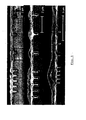
- Figure 1 is representing SEM cross-section image of Electrochemically Deposited Cu at various stages of overfill formation to show the situation of Cu deposition according to the state of the art.
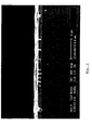
- Figure 2 is representing SEM cross-section image of ECD Cu using the process according to an embodiment the present invention.
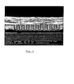
- Figure 3 shows that no overfill is present over dense 0.25 ⁇ m lines with a 3 step process according to a best mode embodiment of the present invention.
- the problems related to the properties of a metal-containing layer deposited by a plating process on ULSI metallization schemes as mentioned in the background of the invention can be avoided by eliminating impurities which are present in the metal plating bath and which are adhered to the surface of the substrate.
- This aspect of method of the invention is not limited to the elimination of impurities in a deposited copper layer but can be valid for a multitude of metal-containing layers which are deposited using a metal plating bath.
- impurities can be defined as compounds being present in a plating bath except the metal source molecules (or ions) and compounds which are adhered on the surface of the substrate.
- the impurities can be additives added to the plating solution to improve the plating of the metal or can be compounds which are accidentally present in the plating bath.
- Typical additives are, but are not limited hereto, so-called suppressor and so-called brighteners.
- a suppressor is known by a person skilled in the art as a surfactant polymer that forms an adsorbed polymeric film on the metal surface such that the free sites are effectively reduced for other bath constituents. Consequently, the growth is suppressed.
- Typical examples are, but are not limited hereto, polymers formulated from polyethylene glycol (PEG),polypropylene glycol (PPG), and many highly branched derivatives thereof.
- a brightener also called accelerator or anti-suppressor
- a brightener enhances Cu deposition, counteracts the action of the suppressor and reduces metal grain size.
- Typical examples are, but are not limited hereto organic disulfides, alkylation derivatives of polyethylene imines.
- Another class of additives are so-called levelers. This class of additives provides a more planar metal-containing layer with less pronounced hillocks.
- additives are organic molecules, organic polymeric molecules and smaller molecules that appear in electrochemical plating baths. These molecules can contain sulfur, carbon, hydrogen or chlorine. Those additives can be incorporated in the deposited metal-containing layer or can be present on the surface of the deposited metal-containing layer. Surprisingly, it was observed that when these materials are incorporated in the metal-containing layer during metal deposition from a plating bath or being present on the surface of the deposited metal-containing layer after deposition from a plating bath, these additives have a negative impact on the quality of the deposited layer. The additives are part of the impurities in or on the surface of the as-deposited film and have a large impact on both the deposition itself, and on subsequent grain growth and processing.
- the adverse effects of the impurities affect the quality of the deposited metal-containing layer.
- hillocks can be formed above trenches or via's because the smaller molecules among the additives in the plating bath accumulate in the trenches and via's which have an accelerating effect on grain growth above these structures even after they've been filled completely. Consequently, CMP of the metal film layer is hampered.
- Other observed problems are: bad adhesion to the layer underlying the metal film, high stress and a high sheet resistance in the deposited metal film.
- the elimination of the impurities can for instance be done by a thermal anneal step or by exposing the deposited layer to several air/vacuum cycles or both.
- a thermal anneal step can be performed in a temperature range higher than room temperature.
- the temperature ranges are typically but not limited to 30-600°C, 50-500°C, 80-400°C, 100-300°C and preferably between 300 and 400°C.
- the time period for the anneal is typically between 5 s and 10 min, 5 s and 5 min, 10 s and 2 min and preferably between 20 s and 90 s.
- the anneals can be performed in a Rapid Thermal Processing furnace or in a conventional furnace under an inert gas ambient (N 2 , Ar, Kr, He, ...) or a H 2 /N 2 ambient or a NH 3 ambient or any other annealing ambient commonly used in semiconductor device processing.
- the air/vacuum cycle is defined as alternately exposing the deposited metal-containing layer to an atmosphere of air or another gas such as N 2 , H 2 , Ar, He, Kr, NH 3 or any mixture thereof at atmospheric pressure and exposing the deposited metal-containing layer to an atmosphere of air or another gas such as N 2 , H 2 , Ar, He, Kr, NH 3 or any mixture thereof or vacuum at a pressure below atmospheric pressure.
- the pressure below atmospheric pressure is typically but not limited to the range between atmospheric pressure and 10 -2 to 10 -4 , 10 -6 and 10 -8 Torr.
- the elimination of the impurities can also be performed at room temperature in an H 2 ambient.
- a method for depositing a metal-containing film from a metal plating bath on a substrate having at least one opening in an insulating layer.
- the opening can be, but is not limited hereto a trench, via, contact hole, bonding path or a capacitor.
- This method comprises the steps of depositing a metal-containing layer from said metal plating bath on said substrate until at least one opening is substantially filled with said metal-containing layer, performing a heating step and/or a vacuum step on said deposited metal-containing layer and depositing another metal, containing layer on said deposited metal containing layer, as defined in claim 1.
- the steps of performing a heating step and/or vacuum step and/or said step of depositing said second metal-containing layer can subsequently be repeated for a number of times in different sequences until all openings are substantially filled with said metal-containing layer.
- the heating or vacuum step is performed to eliminate impurities incorporated in the deposited metal-containing layer or impurities present on the surface of the deposited metal-containing layer.
- the forming of those hillocks can be avoided by first filling the opening with a metal to a thickness that is sufficient to complete the bottom-up fill of the structures with the highest aspect ratio. Afterwards, the impurities present in or on the first metal-containing layer are eliminated by a thermal anneal step or by exposing the deposited layer to several air/vacuum cycles or both. In a following step, further deposition is performed to a thickness sufficient for planarization. In this way, the forming of hillocks is avoided (see Fig. 2) and CMP can easily be performed.
- Another problem that occurs in prior art processing is that the deposited copper films can show a high stress. Exposing the deposited metal-containing layer to a thermal anneal step or several air/vacuum cycles or both will eliminate the impurities and thus reduces the stress.
- the as deposited copper layer according to prior art processing shows a bad adhesion to the underlying layer such as a copper diffusion barrier layer or a dielectric layer.
- Additives like small molecules containing sulfur, carbon or hydrogen can migrate to the interface of the metal-containing layer and the surrounding layers and consequently reduce the adhesion properties. Elimination of those additives (impurities) by exposing the deposited metal-containing layer to a thermal anneal step or several air/vacuum cycles or both will reduce the adhesion problem.
- a Cu barrier layer, a Cu seed layer or another metal-containing layer is deposited in an opening in an insulating layer (step 0).
- the opening in the insulating layer can be an opening with a high aspect ratio, i.e. an aspect ratio of 1/2 or 1/5 or 1/10.
- This opening can also be an opening with a linewidth higher than 5 ⁇ m, i.e. a bonding path or a capacitor.
- the copper barrier layer can be Co, Ta, Ti, TiN, TaN, Si 3 N 4 , W x N or compounds thereof.
- the metal-containing layer can be a cobalt layer.
- ECD electrochemical deposition
- step 2 a further step must be included to eliminate local variations in the concentrations of incorporated species and of those adhered to the surface.
- This may be done by either a thermal anneal or by taking the sample through several air/vacuum cycles (as defined as steps 2a and 2b respectively). This means that the plating should be interrupted. For example, the sample should be taken out of the plating chamber, causing an initial top-down crystallization to occur.
- the thermal anneal method (step 2a) causes much of the material to be cleaned, but also induces a thermal stress and secondary grain growth.
- the air/vacuumcycle removes the unwanted material without causing secondary grain growth, and actually reduces the stress to near-zero values. It is known to reduce concentrations to large depths. Additionally, it may improve adhesion, as the induced diffusion is more one-directional (towards the surface) than for a thermal anneal.
- step 3 the wafer is returned to the ECD-chamber (electro-chemical copper deposition) for further deposition in order to fill large structures to a sufficient thickness for planarization. This is necessary because large structures exhibit conformal filling rather than bottom-up filling.
- the growth obtained in this step will depend on which of the two possibilities in step 2 is chosen, as one causes large grains and thermal stress in the material (according to step 2a), while grains stay relatively small in the other processing mode (step 2b).
- step 5 Before going to the CMP step (called step 5), another anneal (step 4) may be included here to obtain large grains that accelerate the CMP process. It would certainly help to stabilize the structure by preventing self-anneal, thereby making the CMP process independent of the timing of the process itself with respect to the deposition. Also, depending on which process was chosen in step 2, the final grain-size in the trenches and vias may depend on whether an anneal is done before or after CMP as nucleation for growth is different before and after the top layer is removed.
- a final anneal (step 6) may be needed in order to stabilize/optimize the grain-structure.
- a Cu barrier layer, a Cu seed layer or another metal-containing layer is deposited in an opening in an insulating layer using a metal plating bath (step 0).
- the opening in the insulating layer can be an opening with a high aspect ratio, i.e. an aspect ratio of 1/2 or 1/5 or 1/10. This opening can also be an opening with a linewidth higher than 5 ⁇ m, i.e. a bonding path or a capacity.
- the copper barrier layer can be based on Co, Ta, and Ti.
- the metal-containing layer can be a cobalt layer.
- One of the group of the Cu barrier layer, Cu seed layer or another metal-containing layer is deposited on the opening in the insulating layer and do not completely fill the opening (step 1).
- a further step must be included to eliminate local variations in the concentrations of incorporated species (impurities) and of those adhered to the plated surface. This may be done by either a thermal anneal or by taking the sample through several air/vacuum cycles (respectively defined as step 2a and 2b). This means that the plating should be interrupted. For example, the sample must be taken out of the chamber, causing an initial top-down crystallization to occur.
- step 3 deposition of copper from a plating bath proceeds to a thickness that is sufficient to complete the bottom-up fill of the narrow structures.
- a further step can be included to eliminate local variations in the concentrations of incorporated species and of those adhered to the surface. This may be done by either a thermal anneal or by taking the sample through several air/vacuum cycles (respectively defined as step 4a and 4b). For both choices the sample must be taken out of the chamber, causing an initial top-down crystallization to occur.
- the first processing mode (step 4a) causes much of the material to be cleaned, but also induces a thermal stress and secondary grain growth.
- the second processing mode removes the unwanted material without causing secondary grain growth, and actually reduces the stress to near-zero values. It is known to reduce concentrations to large depths. Additionally, it may improve adhesion, as the induced diffusion is more one-directional (towards the surface) than for a thermal anneal.
- step 5 the wafer is returned to the ECD-chamber for further deposition (defined as step 5) in order to fill large structures to a sufficient thickness for planarization. This is necessary because large structures exhibit conformal filling rather than bottom-up filling.
- the growth obtained in this step will depend on which of the two possibilities in steps 2 and 4 was chosen, as one causes large grains and thermal stress in the material (step 2a, 4a), while grains stay relatively small in the other (step 2b, 4b).
- step 4bis another anneal may be included here to obtain large grains that accelerate the CMP process. It would certainly help to stabilize the structure by preventing self-anneal, thereby making the CMP process independent of the timing of the process itself with respect to the deposition. Also, depending on which process mode was chosen in step 2 or 4, the final grain-size in the trenches and vias may depend on whether an anneal is done before or after CMP as nucleation for growth is different before and after the top layer is removed.
- a final anneal may be needed in order to stabilize/optimize the grain-structure (step 6).
- a high-resolution profilometer HRP220 from KLA is used to measure surface topography of the Cu ECD layer deposited overlying patterned dies. Structures with various widths of lines are chosen for this evaluation.
- HRP220 For focussed ion beam (FIB) imaging and SEM pictures, a FEI200 and Philips XL30 are used respectively. Typical resulting structures are shown in Figure 2.
- the sequence that was used for the best mode embodiment consists in inserting an anneal treatment after filling trench to get the same surface grain size and help desorption. This sequence maintains a void-free deposit and limits the increasing step-height undesirable for the CMP process.
- Fig. 3 displays the copper layer overlying dense trench structure according to the best mode processing. A 3-step approach was used as route. It clearly indicates that no "overfill” is observed anymore.
- the processing sequence that was used in detail is as follows :
Landscapes
- Internal Circuitry In Semiconductor Integrated Circuit Devices (AREA)
Claims (8)
- Procédé pour déposer un film contenant du métal à partir d'un bain de métallisation sur un substrat ayant au moins une ouverture dans une couche isolante, comprenant au moins les étapes consistant à :- déposer une couche contenant du métal à partir dudit bain de métallisation sur ledit substrat, pour obtenir une couche déposée contenant du métal, dans au moins une ouverture,- procéder à une étape de chauffage et/ou à une étape d'exposition à un vide sur ladite couche déposée contenant du métal,- déposer une autre couche contenant du métal à partir dudit bain de métallisation sur ladite couche déposée contenant du métal,dans lequel ladite étape de chauffage et/ou ladite étape d'exposition à un vide sont effectuées en vue d'obtenir l'élimination d'impuretés incorporées à ladite couche déposée contenant du métal ou d'impuretés collées à la surface de ladite couche déposée contenant du métal.
- Procédé selon la revendication 1, comprenant également, dans le but de remplir ladite ouverture, l'étape consistant à répéter encore, selon une séquence quelconque, au moins l'une des étapes visant à déposer une couche contenant du métal, à procéder au chauffage et/ou à procéder à une exposition à un vide, un certain nombre de fois jusqu'à ce que toutes les ouvertures de la couche isolante soient substantiellement remplies de ladite couche déposée contenant du métal.
- Procédé selon l'une quelconque des revendications précédentes, dans lequel la couche contenant du métal est une couche de cuivre ou une couche de cobalt.
- Procédé selon l'une quelconque des revendications précédentes, dans lequel l'étape consistant à procéder à une exposition à un vide est réalisée en exposant la couche déposée contenant du métal à un cycle air/vide en exposant alternativement la couche déposée contenant du métal à une atmosphère d'air ou d'un autre gaz, tel que N2, H2, Ar, He, Kr, NH3 ou à n'importe quel mélange contenant un ou plusieurs de ces gaz, à pression atmosphérique, et en exposant la couche déposée contenant du métal à une atmosphère d'air ou d'un autre gaz, tel que N2, H2, Ar, He, Kr, NH3 ou à n'importe quel mélange de ceux-ci ou à un vide, à une pression inférieure à la pression atmosphérique.
- Procédé selon l'une quelconque des revendications précédentes, dans lequel ladite ouverture est une ouverture étroite dans une couche isolante qui fait partie d'une structure de métallisation de type ULSI.
- Procédé selon la revendication 5, dans lequel ladite ouverture étroite appartient au groupe constitué d'une tranchée, d'une ouverture de contact ou d'un trou d'interconnexion dans ladite structure de métallisation de type ULSI.
- Procédé selon l'une quelconque des revendications précédentes, dans lequel on procède, avant l'étape consistant à déposer une couche contenant du métal à partir dudit bain de métallisation sur ledit substrat, à une étape consistant à déposer une couche d'ensemencement contenant du métal.
- Procédé selon l'une quelconque des revendications précédentes, dans lequel ledit bain de métallisation est un bain de métallisation auto-catalytique contenant du métal, ou un bain de métallisation électrolytique contenant du métal.
Priority Applications (1)
| Application Number | Priority Date | Filing Date | Title |
|---|---|---|---|
| EP00870141A EP1063696B1 (fr) | 1999-06-22 | 2000-06-22 | Procédé d'amélioration de la qualité d'une couche déposée contenant du métal à partir d'un bain de métallisation |
Applications Claiming Priority (5)
| Application Number | Priority Date | Filing Date | Title |
|---|---|---|---|
| US14048499P | 1999-06-22 | 1999-06-22 | |
| US140484P | 1999-06-22 | ||
| EP99870194A EP1087432A1 (fr) | 1999-09-24 | 1999-09-24 | Méthode d'amélioration de la qualité d'une couche métallique deposée par un bain de dépôt chimique |
| EP99870194 | 1999-09-24 | ||
| EP00870141A EP1063696B1 (fr) | 1999-06-22 | 2000-06-22 | Procédé d'amélioration de la qualité d'une couche déposée contenant du métal à partir d'un bain de métallisation |
Publications (2)
| Publication Number | Publication Date |
|---|---|
| EP1063696A1 EP1063696A1 (fr) | 2000-12-27 |
| EP1063696B1 true EP1063696B1 (fr) | 2007-08-22 |
Family
ID=27223765
Family Applications (1)
| Application Number | Title | Priority Date | Filing Date |
|---|---|---|---|
| EP00870141A Expired - Lifetime EP1063696B1 (fr) | 1999-06-22 | 2000-06-22 | Procédé d'amélioration de la qualité d'une couche déposée contenant du métal à partir d'un bain de métallisation |
Country Status (1)
| Country | Link |
|---|---|
| EP (1) | EP1063696B1 (fr) |
Cited By (2)
| Publication number | Priority date | Publication date | Assignee | Title |
|---|---|---|---|---|
| US7947163B2 (en) | 2006-07-21 | 2011-05-24 | Novellus Systems, Inc. | Photoresist-free metal deposition |
| US8236160B2 (en) | 2000-08-10 | 2012-08-07 | Novellus Systems, Inc. | Plating methods for low aspect ratio cavities |
Families Citing this family (5)
| Publication number | Priority date | Publication date | Assignee | Title |
|---|---|---|---|---|
| US6534116B2 (en) | 2000-08-10 | 2003-03-18 | Nutool, Inc. | Plating method and apparatus that creates a differential between additive disposed on a top surface and a cavity surface of a workpiece using an external influence |
| JP2004521186A (ja) * | 2000-08-10 | 2004-07-15 | ナトゥール・インコーポレイテッド | 外的影響を用いて加工物の頂部表面とキャビティ表面上に付着する添加物の間に差を作り出すめっき方法および装置 |
| US6858121B2 (en) | 2000-08-10 | 2005-02-22 | Nutool, Inc. | Method and apparatus for filling low aspect ratio cavities with conductive material at high rate |
| US7550070B2 (en) | 2006-02-03 | 2009-06-23 | Novellus Systems, Inc. | Electrode and pad assembly for processing conductive layers |
| US7732329B2 (en) | 2006-08-30 | 2010-06-08 | Ipgrip, Llc | Method and apparatus for workpiece surface modification for selective material deposition |
Family Cites Families (5)
| Publication number | Priority date | Publication date | Assignee | Title |
|---|---|---|---|---|
| US3666549A (en) * | 1969-05-09 | 1972-05-30 | Macdermid Inc | Method of making additive printed circuit boards and product thereof |
| CA1047654A (fr) * | 1974-10-17 | 1979-01-30 | National Research Development Corporation | Electro-deposition sur semi-conducteurs |
| JPS6063987A (ja) * | 1983-09-17 | 1985-04-12 | 沖電気工業株式会社 | 印刷配線基板の製造方法 |
| JP3166221B2 (ja) * | 1991-07-23 | 2001-05-14 | 日本電気株式会社 | 半導体装置及びその製造方法 |
| US5565707A (en) * | 1994-10-31 | 1996-10-15 | International Business Machines Corporation | Interconnect structure using a Al2 Cu for an integrated circuit chip |
-
2000
- 2000-06-22 EP EP00870141A patent/EP1063696B1/fr not_active Expired - Lifetime
Non-Patent Citations (1)
| Title |
|---|
| None * |
Cited By (3)
| Publication number | Priority date | Publication date | Assignee | Title |
|---|---|---|---|---|
| US8236160B2 (en) | 2000-08-10 | 2012-08-07 | Novellus Systems, Inc. | Plating methods for low aspect ratio cavities |
| US7947163B2 (en) | 2006-07-21 | 2011-05-24 | Novellus Systems, Inc. | Photoresist-free metal deposition |
| US8500985B2 (en) | 2006-07-21 | 2013-08-06 | Novellus Systems, Inc. | Photoresist-free metal deposition |
Also Published As
| Publication number | Publication date |
|---|---|
| EP1063696A1 (fr) | 2000-12-27 |
Similar Documents
| Publication | Publication Date | Title |
|---|---|---|
| US6495453B1 (en) | Method for improving the quality of a metal layer deposited from a plating bath | |
| US8709948B2 (en) | Tungsten barrier and seed for copper filled TSV | |
| US7030016B2 (en) | Post ECP multi-step anneal/H2 treatment to reduce film impurity | |
| US6812143B2 (en) | Process of forming copper structures | |
| KR100711526B1 (ko) | 구리 연결선을 갖는 반도체 장치의 제조방법 | |
| US6130161A (en) | Method of forming copper interconnections with enhanced electromigration resistance and reduced defect sensitivity | |
| US6974768B1 (en) | Methods of providing an adhesion layer for adhesion of barrier and/or seed layers to dielectric films | |
| US8766342B2 (en) | Electroless Cu plating for enhanced self-forming barrier layers | |
| US20110259750A1 (en) | Method of direct plating of copper on a ruthenium alloy | |
| EP0881673A2 (fr) | Interconnexions de cuivre inférieures au quart de micron avec une résistance à l'électromigration améliorée et une sensibilité aux défuts réeduite | |
| US20060076244A1 (en) | Barrier enhancement process for copper interconnects | |
| JP5203602B2 (ja) | 銅でないメッキ可能層の上への銅の直接電気メッキのための方法 | |
| TWI696725B (zh) | 用於在反應性金屬膜上電化學沉積金屬的方法(一) | |
| US20060091551A1 (en) | Differentially metal doped copper damascenes | |
| JP2002033323A (ja) | 銅相互接続部を有する半導体デバイスの製造方法 | |
| US6998337B1 (en) | Thermal annealing for Cu seed layer enhancement | |
| US20050274621A1 (en) | Method of barrier layer surface treatment to enable direct copper plating on barrier metal | |
| EP1063696B1 (fr) | Procédé d'amélioration de la qualité d'une couche déposée contenant du métal à partir d'un bain de métallisation | |
| KR20150138086A (ko) | 반응성 금속 필름 상에 금속을 전기화학적으로 증착시키기 위한 방법 | |
| JP2025512235A (ja) | 選択的金属堆積のための選択的阻害 | |
| CN1503344A (zh) | 形成铝金属引线的方法 | |
| KR100672731B1 (ko) | 반도체 소자의 금속배선 형성방법 | |
| JP4937437B2 (ja) | めっき浴から堆積される金属層の特性改善方法 | |
| KR100701673B1 (ko) | 반도체 소자의 구리 배선 형성방법 | |
| KR100456259B1 (ko) | 반도체 소자의 구리 배선 형성방법 |
Legal Events
| Date | Code | Title | Description |
|---|---|---|---|
| PUAI | Public reference made under article 153(3) epc to a published international application that has entered the european phase |
Free format text: ORIGINAL CODE: 0009012 |
|
| AK | Designated contracting states |
Kind code of ref document: A1 Designated state(s): AT BE CH CY DE DK ES FI FR GB GR IE IT LI LU MC NL PT SE |
|
| AX | Request for extension of the european patent |
Free format text: AL;LT;LV;MK;RO;SI |
|
| 17P | Request for examination filed |
Effective date: 20010508 |
|
| AKX | Designation fees paid |
Free format text: AT BE CH CY DE DK ES FI FR GB GR IE IT LI LU MC NL PT SE |
|
| GRAP | Despatch of communication of intention to grant a patent |
Free format text: ORIGINAL CODE: EPIDOSNIGR1 |
|
| GRAS | Grant fee paid |
Free format text: ORIGINAL CODE: EPIDOSNIGR3 |
|
| GRAA | (expected) grant |
Free format text: ORIGINAL CODE: 0009210 |
|
| AK | Designated contracting states |
Kind code of ref document: B1 Designated state(s): AT BE CH CY DE DK ES FI FR GB GR IE IT LI LU MC NL PT SE |
|
| REG | Reference to a national code |
Ref country code: GB Ref legal event code: FG4D |
|
| REG | Reference to a national code |
Ref country code: CH Ref legal event code: EP |
|
| REG | Reference to a national code |
Ref country code: IE Ref legal event code: FG4D |
|
| REF | Corresponds to: |
Ref document number: 60036052 Country of ref document: DE Date of ref document: 20071004 Kind code of ref document: P |
|
| PG25 | Lapsed in a contracting state [announced via postgrant information from national office to epo] |
Ref country code: FI Free format text: LAPSE BECAUSE OF FAILURE TO SUBMIT A TRANSLATION OF THE DESCRIPTION OR TO PAY THE FEE WITHIN THE PRESCRIBED TIME-LIMIT Effective date: 20070822 Ref country code: ES Free format text: LAPSE BECAUSE OF FAILURE TO SUBMIT A TRANSLATION OF THE DESCRIPTION OR TO PAY THE FEE WITHIN THE PRESCRIBED TIME-LIMIT Effective date: 20071203 Ref country code: NL Free format text: LAPSE BECAUSE OF FAILURE TO SUBMIT A TRANSLATION OF THE DESCRIPTION OR TO PAY THE FEE WITHIN THE PRESCRIBED TIME-LIMIT Effective date: 20070822 |
|
| NLV1 | Nl: lapsed or annulled due to failure to fulfill the requirements of art. 29p and 29m of the patents act | ||
| PG25 | Lapsed in a contracting state [announced via postgrant information from national office to epo] |
Ref country code: CH Free format text: LAPSE BECAUSE OF FAILURE TO SUBMIT A TRANSLATION OF THE DESCRIPTION OR TO PAY THE FEE WITHIN THE PRESCRIBED TIME-LIMIT Effective date: 20070822 Ref country code: AT Free format text: LAPSE BECAUSE OF FAILURE TO SUBMIT A TRANSLATION OF THE DESCRIPTION OR TO PAY THE FEE WITHIN THE PRESCRIBED TIME-LIMIT Effective date: 20070822 Ref country code: LI Free format text: LAPSE BECAUSE OF FAILURE TO SUBMIT A TRANSLATION OF THE DESCRIPTION OR TO PAY THE FEE WITHIN THE PRESCRIBED TIME-LIMIT Effective date: 20070822 |
|
| REG | Reference to a national code |
Ref country code: CH Ref legal event code: PL |
|
| ET | Fr: translation filed | ||
| PG25 | Lapsed in a contracting state [announced via postgrant information from national office to epo] |
Ref country code: GR Free format text: LAPSE BECAUSE OF FAILURE TO SUBMIT A TRANSLATION OF THE DESCRIPTION OR TO PAY THE FEE WITHIN THE PRESCRIBED TIME-LIMIT Effective date: 20071123 Ref country code: DK Free format text: LAPSE BECAUSE OF FAILURE TO SUBMIT A TRANSLATION OF THE DESCRIPTION OR TO PAY THE FEE WITHIN THE PRESCRIBED TIME-LIMIT Effective date: 20070822 |
|
| PG25 | Lapsed in a contracting state [announced via postgrant information from national office to epo] |
Ref country code: PT Free format text: LAPSE BECAUSE OF FAILURE TO SUBMIT A TRANSLATION OF THE DESCRIPTION OR TO PAY THE FEE WITHIN THE PRESCRIBED TIME-LIMIT Effective date: 20080122 |
|
| PLBE | No opposition filed within time limit |
Free format text: ORIGINAL CODE: 0009261 |
|
| STAA | Information on the status of an ep patent application or granted ep patent |
Free format text: STATUS: NO OPPOSITION FILED WITHIN TIME LIMIT |
|
| PG25 | Lapsed in a contracting state [announced via postgrant information from national office to epo] |
Ref country code: SE Free format text: LAPSE BECAUSE OF FAILURE TO SUBMIT A TRANSLATION OF THE DESCRIPTION OR TO PAY THE FEE WITHIN THE PRESCRIBED TIME-LIMIT Effective date: 20071122 |
|
| 26N | No opposition filed |
Effective date: 20080526 |
|
| PG25 | Lapsed in a contracting state [announced via postgrant information from national office to epo] |
Ref country code: MC Free format text: LAPSE BECAUSE OF NON-PAYMENT OF DUE FEES Effective date: 20080630 |
|
| PG25 | Lapsed in a contracting state [announced via postgrant information from national office to epo] |
Ref country code: IE Free format text: LAPSE BECAUSE OF NON-PAYMENT OF DUE FEES Effective date: 20080623 |
|
| PG25 | Lapsed in a contracting state [announced via postgrant information from national office to epo] |
Ref country code: CY Free format text: LAPSE BECAUSE OF FAILURE TO SUBMIT A TRANSLATION OF THE DESCRIPTION OR TO PAY THE FEE WITHIN THE PRESCRIBED TIME-LIMIT Effective date: 20070822 |
|
| PG25 | Lapsed in a contracting state [announced via postgrant information from national office to epo] |
Ref country code: LU Free format text: LAPSE BECAUSE OF NON-PAYMENT OF DUE FEES Effective date: 20080622 |
|
| PG25 | Lapsed in a contracting state [announced via postgrant information from national office to epo] |
Ref country code: IT Free format text: LAPSE BECAUSE OF NON-PAYMENT OF DUE FEES Effective date: 20080630 |
|
| REG | Reference to a national code |
Ref country code: FR Ref legal event code: PLFP Year of fee payment: 17 |
|
| REG | Reference to a national code |
Ref country code: FR Ref legal event code: PLFP Year of fee payment: 18 |
|
| PGFP | Annual fee paid to national office [announced via postgrant information from national office to epo] |
Ref country code: DE Payment date: 20170522 Year of fee payment: 18 Ref country code: FR Payment date: 20170523 Year of fee payment: 18 Ref country code: GB Payment date: 20170526 Year of fee payment: 18 |
|
| PGFP | Annual fee paid to national office [announced via postgrant information from national office to epo] |
Ref country code: BE Payment date: 20170524 Year of fee payment: 18 |
|
| REG | Reference to a national code |
Ref country code: DE Ref legal event code: R119 Ref document number: 60036052 Country of ref document: DE |
|
| GBPC | Gb: european patent ceased through non-payment of renewal fee |
Effective date: 20180622 |
|
| REG | Reference to a national code |
Ref country code: BE Ref legal event code: MM Effective date: 20180630 |
|
| PG25 | Lapsed in a contracting state [announced via postgrant information from national office to epo] |
Ref country code: GB Free format text: LAPSE BECAUSE OF NON-PAYMENT OF DUE FEES Effective date: 20180622 Ref country code: DE Free format text: LAPSE BECAUSE OF NON-PAYMENT OF DUE FEES Effective date: 20190101 Ref country code: FR Free format text: LAPSE BECAUSE OF NON-PAYMENT OF DUE FEES Effective date: 20180630 |
|
| PG25 | Lapsed in a contracting state [announced via postgrant information from national office to epo] |
Ref country code: BE Free format text: LAPSE BECAUSE OF NON-PAYMENT OF DUE FEES Effective date: 20180630 |