EP1063703A1 - Circuit pour éviter l'injection de porteurs minoritaires de charge dans un substrat - Google Patents
Circuit pour éviter l'injection de porteurs minoritaires de charge dans un substrat Download PDFInfo
- Publication number
- EP1063703A1 EP1063703A1 EP00111573A EP00111573A EP1063703A1 EP 1063703 A1 EP1063703 A1 EP 1063703A1 EP 00111573 A EP00111573 A EP 00111573A EP 00111573 A EP00111573 A EP 00111573A EP 1063703 A1 EP1063703 A1 EP 1063703A1
- Authority
- EP
- European Patent Office
- Prior art keywords
- circuit
- substrate
- arrangement according
- circuit arrangement
- output terminal
- Prior art date
- Legal status (The legal status is an assumption and is not a legal conclusion. Google has not performed a legal analysis and makes no representation as to the accuracy of the status listed.)
- Withdrawn
Links
Images


Classifications
-
- H—ELECTRICITY
- H10—SEMICONDUCTOR DEVICES; ELECTRIC SOLID-STATE DEVICES NOT OTHERWISE PROVIDED FOR
- H10D—INORGANIC ELECTRIC SEMICONDUCTOR DEVICES
- H10D84/00—Integrated devices formed in or on semiconductor substrates that comprise only semiconducting layers, e.g. on Si wafers or on GaAs-on-Si wafers
- H10D84/80—Integrated devices formed in or on semiconductor substrates that comprise only semiconducting layers, e.g. on Si wafers or on GaAs-on-Si wafers characterised by the integration of at least one component covered by groups H10D12/00 or H10D30/00, e.g. integration of IGFETs
- H10D84/811—Combinations of field-effect devices and one or more diodes, capacitors or resistors
Definitions
- the present invention relates to a circuit arrangement to prevent the injection of minority carriers into the substrate in semiconductor integrated circuits.
- the invention is particularly related to use with junction-insulated integrated circuits in mixed technology with CMOS transistors, DMOS transistors and bipolar transistors suitable.
- CMOS transistors complementary metal-oxide-semiconductor
- DMOS transistors complementary metal-oxide-semiconductor
- bipolar transistors suitable for the isolation of the individual components pn junctions are formed against the substrate, the poles to ensure isolation in the reverse direction have to be. This requires that the substrate at Using a P substrate the lowest potential and at Using an N substrate has the highest potential in the Circuit has. A P-substrate is usually used for this grounded.
- the circuit arrangement at least one Switch to connect between an output terminal and a substrate connection of the semiconductor circuit.
- the output terminal of the semiconductor circuit is, for example external circuit can be controlled.
- the circuit arrangement furthermore has a control circuit with an input terminal to supply one of a potential at the Output terminal of the semiconductor signal dependent input signal and with an output terminal to control the Switch depending on the input signal.
- the potential at the output terminal also drops with circuits a P-substrate below the value of the substrate potential or the potential increases in circuits with an N-substrate the output terminal via the value of the substrate potential the switch closes controlled by the control circuit, whereby the substrate potential the value of the potential assumes at the output terminal.
- the circuit arrangement preferably has a second one Switch on between a reference potential and the substrate connection connectable and by means of a second output terminal the control circuit can be controlled.
- An input terminal the control circuit is preferably a second input signal dependent on the reference potential.
- the output terminals are preferably directly to the input terminals connected to the evaluation circuit.
- the input signals then correspond to the potentials at the respective output terminals.
- the evaluation circuit has a Comparator based on the potentials at the output terminals or compares the dependent input signals, where activation of the switches depending on the comparison result he follows. Is the potential at a P-substrate at the at least one output terminal less than the reference potential or in the case of an N substrate, the potential is at least an output terminal larger than the reference potential the switch connected to the output terminal closes and put the substrate on the opposite of the reference potential lower or higher potential. Otherwise it connects the reference potential connected switch, creating the substrate connected to the reference potential - usually ground potential is.
- the circuit arrangement has preferably further switches, each between Output connections of the semiconductor circuit and their Substrate connection can be connected.
- the switches are over further output terminals of the control circuit can be controlled.
- the control circuit has further input terminals, which others dependent on the potentials at the output terminals Input signals can be supplied, with a control the switch depends on a comparison of the input signals he follows. Activated by the control circuit closes the switch on a P substrate to the output terminal with the lowest potential and with an N substrate connected to the output terminal with the highest potential is.
- the control circuit shows a comparison of the input signals a comparator circuit with one of the number of input terminals corresponding number of transistors, each time a transistor with a load path connection to an input terminal is connected and being the control connections of the transistors connected to a common current source are.
- a power source is preferably connected as a load.
- an output signal can be tapped to control the switches.
- FIG. 1 an output stage of a semiconductor integrated circuit shown.
- Figure 1a shows a section Cross section through a semiconductor body in which the circuit 1b shows the electrical circuit diagram of the section of the semiconductor body shown in Figure 1a.
- Figure 1a is a cross section through a semiconductor body shown, which is based on a P-substrate SUB and in which in mixed technology CMOS transistors, DMOS transistors and Bipolar transistors can be implemented.
- CMOS transistors complementary metal-oxide-semiconductors
- Bipolar transistors can be implemented.
- Over the substrate SUB is an n-doped layer 10, preferably an epitaxial layer, upset.
- n-doped layer 10 preferably an epitaxial layer, upset.
- a DMOS transistor is formed in the semiconductor body. Is to a p-doped well 12 is introduced into the n-doped layer 10, into which in turn two n-doped wells 14, 16 are introduced are that serve as source areas and that over a conductive material 17 can be contacted.
- annular gate electrode 18, G is above of the semiconductor body, of this by a not shown Insulation layer separated, arranged.
- the drain area of the MOSFET is through a heavily n-doped region 28 between substrate SUB and layer 10 and a heavily n-doped Region 26, which extends upwards from region 28, educated.
- Figure 1a there are two p-doped regions 22, 24 shown to isolate the MOSFET from neighboring components serve.
- FIG. 2 shows an embodiment of an inventive Circuit arrangement for preventing the injection of minority charge carriers integrated into the substrate SUB Semiconductor circuits.
- the circuit arrangement is between at least one output terminal A1; A2 and the substrate of the Semiconductor circuit arrangement connectable.
- FIG. 2 shows two output stages OUT1 by way of example, OUT2 of a semiconductor integrated circuit, which of the in Figure 1 described type are shown.
- OUT2 serves a MOSFET M1, M2 of each output stage OUT1, OUT2 as a low-side switch for connecting one to an output terminal A1, A2 connectable load to a reference potential M.
- D1, D2 those inevitably formed in the semiconductor body Diodes between the drain connections of MOSFET M1, M2 and the substrate SUB.
- the substrate connection SUB of the semiconductor circuit can for example by a contact ring around all Low-side switches M1, M2 are formed in the semiconductor body be, with substrate areas removed by low-side switches are, for example, permanently connected to the reference potential can be. There is also the option of all Substrate contacts in the semiconductor switch to a common Connect substrate connection.
- the second variant is more suitable for integrated circuits where the Chip on the back is connected to ground.
- the first variant is suitable for chips whose back is no more has electrical connection.
- the circuit arrangement according to the invention has a first one Switch S1 on, which is between an output terminal A1 and a Substrate connection SUB of the semiconductor circuit can be connected is.
- a control circuit AS is used to control the Switch S1 via a first output terminal AK1.
- the control takes place depending on a feedable to an input terminal EK1 Input signal ES1, which from a potential the output terminal A1 is dependent.
- the input terminal EK1 is in the embodiment to a terminal of the switch S1 and can therefore be connected directly to output terminal A1.
- a second switch S2 is between the substrate connection SUB and a reference potential M can be connected. For its control is the second switch S2 to a second output terminal AK2 of the control circuit connected. A second Input terminal EK2 is dependent on the reference potential M.
- second input signal ES2 in the exemplary embodiment the reference potential M itself as the input signal ES2 directly, fed.
- Another switch S3 is between another output terminal A2 and the substrate connection SUB can be connected.
- To its control is the further switch S3 to another Output terminal AK3 of the control circuit connected, wherein a further input terminal EK3 of the control circuit to a terminal of switch S3 and thus to the output terminal A2 for supplying one of the potential at the output terminal A2 dependent input signal ES3 connected is.
- the control circuit compares the input signals ES1, ES2, ES3 or the potentials at the output terminals A1, A2 and the reference potential M and closes the switch S1; S2; S3, which in the exemplary embodiment has the lowest potential connected.
- Ground potential is usually selected as the reference potential M, which should be lower than that in normal operation Potentials at the output terminals A1, A2.
- the second switch S2 is closed and places the substrate SUB to reference potential M.
- the potential at one of the output terminals drops A1; A2 due to one connected to it external circuit below the reference potential M, the Switch S2 opened and the to this output A1; A2 connected Switch S1; S3 closed and thus puts that Substrate SUB to this lower potential. This will prevents that between the output A1; A2 and the substrate SUB formed diode D1; D2 conducts and minority carriers be injected into the substrate SUB.
- a resistor R SUB connected between the substrate connection SUB and the reference potential M has the effect that the substrate SUB assumes a defined value when switched on, if none of the switches S1, S2, S3 is closed.
- the resistance is about 50-500 ohms. The resistance is selected so that the on-resistance of the switches S1, S2, S2 is at most 1/5 of the resistance value of the resistor R SUB .
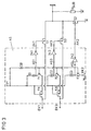
- FIG. 3 shows an embodiment of a control circuit AS to control switches S1, S2, S3.
- the control circuit AS has one of the number of input terminals EK1, EK2, EK3 corresponding number of transistors T1, T2, T3, -in the example of npn bipolar transistors.
- the emitter connection one of the transistors T1, T2, T3 is on one of the input terminals EK1; EK2; EK3 connected.
- As Protection against overvoltage is between the first input terminal EK1 and the transistor T1 and the further input terminal EK3 and the transistor T2 each connected a MOSFET T11, T12, whose gate electrode is connected to a supply potential V + is.
- the use of the MOSFET T11, T12 is optional. It can be dispensed with if ensured is that at the input terminals EK1, EK3 none of the transistors T1, T2 destructive voltage can be present.
- the base connections of the transistors T1, T2, T3 are connected to one common power source IB connected. As a load is between the collector terminal K of each of the transistors T1, T2, T3 and the supply potential V + each have a current source I1, I2, I3 switched.
- Control signals AS1, AS2, AS3 for controlling the switches are at the collector terminals of transistors T1, T2, T3 tapped, the control signals in the exemplary embodiment AS1, AS2, AS3 inverted by inverter IN1, IN2, IN3 at the output terminals AK1, AK2, AK3 to control the Switches S1, S2, S3 are available.
- the switches are formed in the example as an n-channel MOSFET, whose gate connections connected to the output terminals AK1, AK2, AK3 are.
- the drive circuit shown works as follows described.
- T1; T2; T3 From the to the various input terminals EK1, EK2, EK3 connected bipolar transistors T1, T2, T3 conducts only the one whose emitter electrode is at the lowest potential lies.
- This transistor T1; T2; T3 takes over approximately the entire current of the current source IB and is up turned on for saturation, the other transistors T1; T2; Lock T3.
- the reference potential M serves as the reference variable Transistors T1 and T2 can only conduct if the potential at the input terminals EK1, EK3 lower than the reference potential M is, otherwise the transistor T2 conducts.
- the potential at Collector connection of the conductive transistor T1; T2; T3 drops to a low value, while the potentials of the collector connections the non-conductive transistors T1; T2; T3 approximately at the value of the supply potential V + stay.
- the inverter downstream of the collector connection IN1; IN 2; IN3 generates from the low level at the collector electrode of the conductive transistor is high, the is sufficient, the connected switch S1; S2; S3 close.
- the circuit arrangement according to the invention is designed in such a way that they are only connected to an output terminal of the semiconductor circuit can be connected, are for the control circuit AS only two bipolar transistors, one for connection to the input terminal connected to the output terminal and one to be provided for connection to reference potential. Accordingly only two switches are to be provided, one for connecting the Substrate to the output terminal and one for connecting the Substrate at reference potential. Because in this case there is always one the two switches must conduct, it is sufficient in the control circuit a control signal at the collector connection only one of the two bipolar transistors, described in FIG. 3 Way to tap to drive one of the switches.
- the other switch has an inverse control signal feed, which can be tapped before the inverter. To this An inverter can be used in this embodiment save on.
- the circuit arrangement according to the invention was in the exemplary embodiments without limitation of generality for a semiconductor circuit based on a substrate described. It is of course also for semiconductor circuits usable, which are based on an N-substrate.
- the control circuit is designed so that only the switch leads to the input terminal with the highest potential connected.
Landscapes
- Semiconductor Integrated Circuits (AREA)
- Electronic Switches (AREA)
- Metal-Oxide And Bipolar Metal-Oxide Semiconductor Integrated Circuits (AREA)
Applications Claiming Priority (2)
| Application Number | Priority Date | Filing Date | Title |
|---|---|---|---|
| DE19928762 | 1999-06-23 | ||
| DE19928762A DE19928762C1 (de) | 1999-06-23 | 1999-06-23 | Schaltungsanordnung zur Verhinderung der Injektion von Minoritätsladungsträgern in das Substrat |
Publications (1)
| Publication Number | Publication Date |
|---|---|
| EP1063703A1 true EP1063703A1 (fr) | 2000-12-27 |
Family
ID=7912262
Family Applications (1)
| Application Number | Title | Priority Date | Filing Date |
|---|---|---|---|
| EP00111573A Withdrawn EP1063703A1 (fr) | 1999-06-23 | 2000-05-30 | Circuit pour éviter l'injection de porteurs minoritaires de charge dans un substrat |
Country Status (2)
| Country | Link |
|---|---|
| EP (1) | EP1063703A1 (fr) |
| DE (1) | DE19928762C1 (fr) |
Families Citing this family (3)
| Publication number | Priority date | Publication date | Assignee | Title |
|---|---|---|---|---|
| DE10006519B4 (de) * | 2000-02-15 | 2004-03-11 | Infineon Technologies Ag | MOSFET-Treibertransistor und Verfahren zum Herstellen desselben |
| US7470955B2 (en) | 2005-04-15 | 2008-12-30 | Delphi Technologies, Inc. | Technique for improving negative potential immunity of an integrated circuit |
| US7436223B2 (en) | 2005-10-28 | 2008-10-14 | Delphi Technolopgies, Inc. | Technique for improving negative potential immunity of an integrated circuit |
Citations (5)
| Publication number | Priority date | Publication date | Assignee | Title |
|---|---|---|---|---|
| US4109161A (en) * | 1976-02-09 | 1978-08-22 | Nippon Electric Company, Ltd. | Memory circuit with protection circuit |
| EP0703620A1 (fr) * | 1994-09-21 | 1996-03-27 | STMicroelectronics S.r.l. | Circuit pour prévenir l'amorçage de composants parasites dans des circuits intégrés comprenant un étage de puissance et un circuit de commande basse tension |
| EP0788163A2 (fr) * | 1996-02-05 | 1997-08-06 | Kabushiki Kaisha Toshiba | Dispositif de circuit intégré à semi-conducteur |
| EP0847089A1 (fr) * | 1996-12-09 | 1998-06-10 | STMicroelectronics S.r.l. | Méthode et dispositif pour supprimer des effets parasites dans un circuit integré avec des jonctions d'isolation |
| US5872479A (en) * | 1995-06-28 | 1999-02-16 | Lg Semicon Co., Ltd. | Apparatus for regulating substrate voltage in semiconductor device |
Family Cites Families (1)
| Publication number | Priority date | Publication date | Assignee | Title |
|---|---|---|---|---|
| DE19518524C2 (de) * | 1995-05-19 | 1997-03-20 | Siemens Ag | Schaltungsanordnung zur Verringerung einer Minoritätsträgerinjektion in ein Substrat |
-
1999
- 1999-06-23 DE DE19928762A patent/DE19928762C1/de not_active Expired - Fee Related
-
2000
- 2000-05-30 EP EP00111573A patent/EP1063703A1/fr not_active Withdrawn
Patent Citations (5)
| Publication number | Priority date | Publication date | Assignee | Title |
|---|---|---|---|---|
| US4109161A (en) * | 1976-02-09 | 1978-08-22 | Nippon Electric Company, Ltd. | Memory circuit with protection circuit |
| EP0703620A1 (fr) * | 1994-09-21 | 1996-03-27 | STMicroelectronics S.r.l. | Circuit pour prévenir l'amorçage de composants parasites dans des circuits intégrés comprenant un étage de puissance et un circuit de commande basse tension |
| US5872479A (en) * | 1995-06-28 | 1999-02-16 | Lg Semicon Co., Ltd. | Apparatus for regulating substrate voltage in semiconductor device |
| EP0788163A2 (fr) * | 1996-02-05 | 1997-08-06 | Kabushiki Kaisha Toshiba | Dispositif de circuit intégré à semi-conducteur |
| EP0847089A1 (fr) * | 1996-12-09 | 1998-06-10 | STMicroelectronics S.r.l. | Méthode et dispositif pour supprimer des effets parasites dans un circuit integré avec des jonctions d'isolation |
Also Published As
| Publication number | Publication date |
|---|---|
| DE19928762C1 (de) | 2000-11-23 |
Similar Documents
| Publication | Publication Date | Title |
|---|---|---|
| DE68905269T2 (de) | MOS-Transistor und Anwendung bei einer Freilaufdiode. | |
| DE2411839C3 (de) | Integrierte Feldeffekttransistor-Schaltung | |
| DE3838962C2 (fr) | ||
| EP0538507B1 (fr) | Circuit de protection pour contacts de connexion de circuits intégrés monolithiques | |
| EP1714321A2 (fr) | Montage et procede pour proteger un circuit integre a semi-conducteur | |
| DE19814675A1 (de) | Ausgabeschaltung für einen Leistungs-IC mit hoher Durchbruchsspannung | |
| DE112004002717B4 (de) | Pufferschaltung und Pufferschaltungsanordnung mit elektrostatischem Entladeschutz | |
| DE10223950B4 (de) | MOS-Leistungstransistor | |
| DE19932959B4 (de) | Halbleitervorrichtung und diese verwendende Halbleiterschaltung | |
| DE69624493T2 (de) | Vorrichtung und Verfahren zur Unterdrückung von parasitären Effekten in einer integrierten Schaltung mit pn-Isolationszonen | |
| EP0174473B1 (fr) | Etage de sortie de puissance intégré monolithiquement | |
| DE10061589C1 (de) | Schaltungsanordnung mit Integriertem Verstärker | |
| DE69426565T2 (de) | Schaltung zur Verhinderung des Durchschaltens von parasitären Bauelementen in integrierten Schaltungen bestehend aus einer Leistungsstufe un einer Niederspannungssteuerschaltung | |
| DE102005000801A1 (de) | Vorrichtung, Anordnung und System zum ESD-Schutz | |
| DE60004008T2 (de) | Halbleiterschaltung mit einem Bauelement mit isoliertem Gate und einer zugehörigen Kontrollschaltung | |
| DE1926182A1 (de) | Monolithische integrierte Halbleiterschaltung | |
| DE2852200A1 (de) | Integrierte logische schaltung | |
| DE19928762C1 (de) | Schaltungsanordnung zur Verhinderung der Injektion von Minoritätsladungsträgern in das Substrat | |
| WO2001020677A1 (fr) | Dispositif de protection contre les decharges electrostatiques pour entrees et sorties de signaux avec tolerance vis-a-vis des surtensions | |
| EP0732810A2 (fr) | Commutateur semi-conducteur commandable | |
| EP0826241B1 (fr) | Circuiterie permettant de reduire une injection de porteur minoritaire dans un substrat | |
| EP1285483B1 (fr) | Composant semi-conducteur | |
| EP0562354A2 (fr) | Dispositif de circuit intégré | |
| DE3246810A1 (de) | Steuerschaltung fuer gategesteuerte diodenschalter | |
| DE10340603B4 (de) | Schaltungsanordnung und Spannungsregeleinrichtung mit Schaltungsanordnung |
Legal Events
| Date | Code | Title | Description |
|---|---|---|---|
| PUAI | Public reference made under article 153(3) epc to a published international application that has entered the european phase |
Free format text: ORIGINAL CODE: 0009012 |
|
| AK | Designated contracting states |
Kind code of ref document: A1 Designated state(s): AT DE FR GB IT |
|
| AX | Request for extension of the european patent |
Free format text: AL;LT;LV;MK;RO;SI |
|
| 17P | Request for examination filed |
Effective date: 20010608 |
|
| AKX | Designation fees paid |
Free format text: AT DE FR GB IT |
|
| 17Q | First examination report despatched |
Effective date: 20060814 |
|
| STAA | Information on the status of an ep patent application or granted ep patent |
Free format text: STATUS: THE APPLICATION IS DEEMED TO BE WITHDRAWN |
|
| 18D | Application deemed to be withdrawn |
Effective date: 20070227 |