EP1065567A2 - Integrierte Kontrolle einer kritischen Dimension - Google Patents
Integrierte Kontrolle einer kritischen Dimension Download PDFInfo
- Publication number
- EP1065567A2 EP1065567A2 EP00113788A EP00113788A EP1065567A2 EP 1065567 A2 EP1065567 A2 EP 1065567A2 EP 00113788 A EP00113788 A EP 00113788A EP 00113788 A EP00113788 A EP 00113788A EP 1065567 A2 EP1065567 A2 EP 1065567A2
- Authority
- EP
- European Patent Office
- Prior art keywords
- waveform
- target
- parameter values
- wafer
- process parameter
- Prior art date
- Legal status (The legal status is an assumption and is not a legal conclusion. Google has not performed a legal analysis and makes no representation as to the accuracy of the status listed.)
- Withdrawn
Links
Images




Classifications
-
- G—PHYSICS
- G03—PHOTOGRAPHY; CINEMATOGRAPHY; ANALOGOUS TECHNIQUES USING WAVES OTHER THAN OPTICAL WAVES; ELECTROGRAPHY; HOLOGRAPHY
- G03F—PHOTOMECHANICAL PRODUCTION OF TEXTURED OR PATTERNED SURFACES, e.g. FOR PRINTING, FOR PROCESSING OF SEMICONDUCTOR DEVICES; MATERIALS THEREFOR; ORIGINALS THEREFOR; APPARATUS SPECIALLY ADAPTED THEREFOR
- G03F7/00—Photomechanical, e.g. photolithographic, production of textured or patterned surfaces, e.g. printing surfaces; Materials therefor, e.g. comprising photoresists; Apparatus specially adapted therefor
- G03F7/70—Microphotolithographic exposure; Apparatus therefor
- G03F7/70483—Information management; Active and passive control; Testing; Wafer monitoring, e.g. pattern monitoring
- G03F7/7055—Exposure light control in all parts of the microlithographic apparatus, e.g. pulse length control or light interruption
- G03F7/70558—Dose control, i.e. achievement of a desired dose
-
- H—ELECTRICITY
- H10—SEMICONDUCTOR DEVICES; ELECTRIC SOLID-STATE DEVICES NOT OTHERWISE PROVIDED FOR
- H10P—GENERIC PROCESSES OR APPARATUS FOR THE MANUFACTURE OR TREATMENT OF DEVICES COVERED BY CLASS H10
- H10P74/00—Testing or measuring during manufacture or treatment of wafers, substrates or devices
-
- G—PHYSICS
- G03—PHOTOGRAPHY; CINEMATOGRAPHY; ANALOGOUS TECHNIQUES USING WAVES OTHER THAN OPTICAL WAVES; ELECTROGRAPHY; HOLOGRAPHY
- G03F—PHOTOMECHANICAL PRODUCTION OF TEXTURED OR PATTERNED SURFACES, e.g. FOR PRINTING, FOR PROCESSING OF SEMICONDUCTOR DEVICES; MATERIALS THEREFOR; ORIGINALS THEREFOR; APPARATUS SPECIALLY ADAPTED THEREFOR
- G03F7/00—Photomechanical, e.g. photolithographic, production of textured or patterned surfaces, e.g. printing surfaces; Materials therefor, e.g. comprising photoresists; Apparatus specially adapted therefor
- G03F7/70—Microphotolithographic exposure; Apparatus therefor
- G03F7/70483—Information management; Active and passive control; Testing; Wafer monitoring, e.g. pattern monitoring
- G03F7/70605—Workpiece metrology
- G03F7/70616—Monitoring the printed patterns
- G03F7/70625—Dimensions, e.g. line width, critical dimension [CD], profile, sidewall angle or edge roughness
-
- G—PHYSICS
- G03—PHOTOGRAPHY; CINEMATOGRAPHY; ANALOGOUS TECHNIQUES USING WAVES OTHER THAN OPTICAL WAVES; ELECTROGRAPHY; HOLOGRAPHY
- G03F—PHOTOMECHANICAL PRODUCTION OF TEXTURED OR PATTERNED SURFACES, e.g. FOR PRINTING, FOR PROCESSING OF SEMICONDUCTOR DEVICES; MATERIALS THEREFOR; ORIGINALS THEREFOR; APPARATUS SPECIALLY ADAPTED THEREFOR
- G03F7/00—Photomechanical, e.g. photolithographic, production of textured or patterned surfaces, e.g. printing surfaces; Materials therefor, e.g. comprising photoresists; Apparatus specially adapted therefor
- G03F7/70—Microphotolithographic exposure; Apparatus therefor
- G03F7/70483—Information management; Active and passive control; Testing; Wafer monitoring, e.g. pattern monitoring
- G03F7/70605—Workpiece metrology
- G03F7/70616—Monitoring the printed patterns
- G03F7/70641—Focus
-
- H—ELECTRICITY
- H10—SEMICONDUCTOR DEVICES; ELECTRIC SOLID-STATE DEVICES NOT OTHERWISE PROVIDED FOR
- H10P—GENERIC PROCESSES OR APPARATUS FOR THE MANUFACTURE OR TREATMENT OF DEVICES COVERED BY CLASS H10
- H10P72/00—Handling or holding of wafers, substrates or devices during manufacture or treatment thereof
- H10P72/06—Apparatus for monitoring, sorting, marking, testing or measuring
- H10P72/0604—Process monitoring, e.g. flow or thickness monitoring
-
- H—ELECTRICITY
- H10—SEMICONDUCTOR DEVICES; ELECTRIC SOLID-STATE DEVICES NOT OTHERWISE PROVIDED FOR
- H10P—GENERIC PROCESSES OR APPARATUS FOR THE MANUFACTURE OR TREATMENT OF DEVICES COVERED BY CLASS H10
- H10P74/00—Testing or measuring during manufacture or treatment of wafers, substrates or devices
- H10P74/23—Testing or measuring during manufacture or treatment of wafers, substrates or devices characterised by multiple measurements, corrections, marking or sorting processes
Definitions
- the present invention relates to a method and apparatus for monitoring and controlling processing in particular, carried out on a semiconductor substrate, and more particularly for controlling critical dimensions (CDs) of features formed on the semiconductor substrate through feedback and feed-forward of information gathered during in-process inspection of the features.
- CDs critical dimensions
- the invention has particular applicability for in-line inspection of semiconductor wafers during manufacture of high-density semiconductor devices with submicron design features.
- photolithography wherein masks are used to transfer circuitry patterns to semiconductor wafers.
- a series of such masks are employed in a preset sequence.
- Each photolithographic mask includes an intricate set of geometric patterns corresponding to the circuit components to be integrated onto the wafer.
- Each mask in the series is used to transfer its corresponding pattern onto a photosensitive layer (i.e., a photoresist layer) which has been previously coated on a layer, such as a polysilicon or metal layer, formed on the silicon wafer.
- the transfer of the mask pattern onto the photoresist layer is conventionally performed by an optical exposure tool such as a scanner or a stepper, which directs light or other radiation through the mask to expose the photoresist.
- the photoresist is thereafter developed to form a photoresist mask, and the underlying polysilicon or metal layer is selectively etched in accordance with the mask to form features such as lines or gates.
- Fabrication of the mask follows a set of predetermined design rules set by processing and design limitations. These design rules define the space tolerance between devices and interconnecting lines and the width of the lines themselves, to ensure that the devices or lines do not overlap or interact with one another in undesirable ways.
- the design rule limitation is referred to as the critical dimension ("CD"), defined as the smallest width of a line or the smallest space between two lines permitted in the fabrication of the device.
- CD critical dimension
- the CD for most ultra large scale integration applications is on the order of a fraction of a micron.
- Deviations of a feature's CD and profile from design dimensions may adversely affect the performance of the finished semiconductor device.
- the measurement of a feature's CD and profile may indicate processing problems, such as stepper defocusing or photoresist loss due to over-exposure.
- CD and profile values, and the variation of feature CD from design dimensions, are important indicators of the accuracy and stability of the photoresist and etch processes, and "CD control" to reduce such variation is an important part of semiconductor processing.
- CD control necessarily involves monitoring and adjusting both the photolithography and etch processes to address CD variations from field to field (FTF) within a wafer, from wafer to wafer (WTW) and from lot to lot (LTL).
- FTF field to field
- WTW and LTL variation FTF and LTL are dominant variation components, while WTW typically counts for less than 10% of the total CD variation.
- FTF variation is generally determined by process tool performance, such as photoresist coating and baking uniformity, stepper or scanner stage leveling, and etch micro-loading uniformity.
- LTL variation is generally determined by process stability, including process equipment stability.
- CD-SEM critical dimension scanning electron microscope
- the present invention intends to overcome the above problems.
- the object is solved by the method and apparatus for controlling processing according to independent claims 1 and 23 and by the computer readable medium according to independent claim 12.
- the present invention generally relates to a method and apparatus for controlling processing. In particular it relates to controlling processing carried out on semiconductor substrates. More particularly, the present invention relates to controlling critical dimensions (CDs) of features formed on the semiconductor substrate through feedback and feed-forward of information gathered during in-process inspection of the features.
- CDs critical dimensions
- the invention has particular applicability for in-line inspection of semiconductor wafers during manufacture of high-density semiconductor devices with submicron design features.
- An advantage of the present invention is the ability to reduce lot to lot CD variations in semiconductor wafers without reducing production throughput, by utilizing information gathered during in-process inspection of the wafers.
- a method of controlling the processing of a semiconductor wafer comprises performing a first process on the wafer and obtaining characteristics of a target feature on the wafer formed using the first process.
- a set of process parameter values for a second process is determined based on the target feature characteristics, and the second process is then performed on the wafer based on the second process parameter values.
- a set of process parameter values is determined for the first process responsive to the target feature characteristics, and the first process is performed on another semiconductor wafer responsive to the first process parameter values.
- Another aspect of the present invention is an apparatus for carrying out the steps of the above method.
- a still further aspect of the present invention is a computer-readable medium bearing instructions for controlling the processing of a semiconductor wafer, the instructions, when executed, being arranged to cause one or more processors to perform the steps of the above method.
- the present invention addresses the problem of CD control by reducing the lot to lot CD variation by feeding back information gathered during inspection of a wafer (e.g., after photoresist development) to upcoming lots that will be going through the photolithography process, and by feeding forward information to adjust the next process the inspected wafer will undergo (e.g., the etch process).
- a feature such as an etch mask is formed on a lot or batch of semiconductor wafers at a "photo cell" by a photolithography process (e.g., exposure at a stepper followed by photoresist development)
- a photolithography process e.g., exposure at a stepper followed by photoresist development
- one or more wafers of the lot are chosen for inspection and the feature is conventionally imaged, typically at several sites on each wafer to be inspected, with a CD-SEM to measure its CD and other sensitive parameters such as edge width and profile grade, and to obtain its SEM waveform.
- the measured parameters are linked to photolithography adjustable parameters such as stepper focus and exposure settings.
- the linked information on focus and exposure can be fed back to the photo cell so the stepper can be adjusted, either automatically or at the user's discretion, to correct the deviation in following lots.
- the measured parameters are also linked to etch process adjustable parameters such as etch recipes for different over-etch and/or etch chemistry. Therefore, if the measured parameters deviate from desired values, a linked etch recipe to correct the error can be fed forward to the etcher, which recipe can be implemented automatically or at the user's discretion to process the wafers in the inspected lot.
- the feedback and feed-forward mechanism of the present invention improves lot to lot CD control at inspection following photoresist development and at final inspection.
- a "library" of reference waveforms such as conventional SEM waveforms, is created by imaging a plurality of reference features formed, as on a test wafer in the photo cell, using the reticle which will be used in producing the features to be inspected.
- Each of the reference features is formed using different process parameters, such as different stepper focus and exposure settings.
- the profile of each of the reference features is imaged, if desired, as by a cross-section FIB-SEM.
- each reference SEM waveform is associated with known stepper settings and, optionally, a known profile.
- an etch recipe that will compensate for deviations in the reference feature is linked to each reference feature.
- the reference waveform associated with the particular cross-section SEM waveform having optimal CD, profile and/or other characteristics is chosen and identified as a "golden waveform".
- a feature of unknown CD is conventionally imaged with an SEM, and the resulting waveform is compared to the golden waveform. If the feature's waveform does not substantially match the golden waveform, it is compared to the reference feature waveforms to find the closest matching reference waveform.
- the profile and stepper settings of the matching reference waveform (which correspond to the profile and stepper settings of the feature under inspection) can then be compared to those associated with the golden waveform and fed back to the photo cell for automatic or manual process adjustment.
- the etch recipe of the matching reference waveform can be fed forward to the etcher to adjust the CDs of the features of the wafers in the lot under inspection resulting from the etch process.
- stepper focus and exposure settings of sample features from a lot under inspection are pinpointed, and an optimal etch recipe for the lot determined, by obtaining each feature's SEM waveform and comparing the waveform to a library of reference feature waveforms, thereby enabling feedback to the photo cell and feed-forward to the etcher to adjust process parameters to reduce lot to lot CD variation.
- the library of reference waveforms is formed as a focus exposure matrix ("FEM") on a test wafer, which is a conventional technique for obtaining the best exposure/focus combination when new masks are produced or after a change in the fabrication recipe; i.e., to optimize the process by finding the combination of stepper focus and exposure which results in the best resolution on the wafer, in keeping with the required CD.
- the FEM procedure typically comprises sequentially exposing a series of areas of the test wafer with the pattern of the mask, while exposure and focus values are incrementally changed from one exposure location to the next Specifically, the test wafer is exposed in a stepper while the focus is varied along one axis and the exposure is varied along the other.
- a matrix of features is obtained on the exposed wafer, wherein each exposure site or die has a different focus-exposure setting.
- Figure 1 illustrates a portion of a focus-exposure matrix.
- the matrix 101 is formed by patterning the wafer surface using light or other radiation passing through the mask.
- a single wafer may include tens or hundreds of dies depending on die size, each of which corresponds to one of the exposure areas, or "cells", shown in Fig. 1. For convenience, only a small number of the dies are illustrated.
- Each of the cells of the matrix has an incrementally different exposure E and/or was formed with an incrementally different focus f than any of the surrounding cells, as referenced by nomenclature f n E m in the drawings.
- the focus is varied along one axis while the exposure is varied along the other axis in the formation of the matrix.
- the individual exposure sites are developed and then examined with a conventional CD-SEM scan to measure the feature's CD, and the resulting waveforms stored to obtain a reference waveform for each site.
- the exposure sites can then be imaged, if desired, with an atomic force microscope (AFM) or sectioned and imaged with a cross-section FIB-SEM to determine their respective profiles.
- An evaluation of the CD, cross-sectional profile images, and other measured parameters is performed to determine the combination of focus and exposure settings which produces the best feature characteristics.
- the reference waveform i.e., conventional SEM waveform
- a golden waveform i.e., conventional SEM waveform
- Each reference waveform is further associated with an etch recipe experimentally determined to be the optimal recipe to produce a finished feature (after etching) with a CD as close as possible to design dimensions, given the measured CD and other characteristics of the reference feature (i.e., the etch mask).
- Figs. 2A and 2B The concept of the reference library of the present invention is illustrated in Figs. 2A and 2B.
- Fig. 2A which is based on the FEM of Fig. 1, the optimized process condition is represented by the cell marked "x". All other cells preferably cover a reasonable range of process variation, or the "process window", wherein ⁇ f n and ⁇ E m are each measured as the difference from cell x; that is, ⁇ f and ⁇ E are both zero in cell x, and ⁇ f and ⁇ E of the other cells are exposure doses and focus settings relative to the optimal exposure and focus.
- Each exposure column A-E represents a different etch recipe. Since the etch recipe adjustment applies only to CD, not profile, the etch recipes' assignments are aligned with the exposure columns.
- Fig. 2A which is based on the FEM of Fig. 1
- the optimized process condition is represented by the cell marked "x”. All other cells preferably cover a reasonable range of process variation, or the "process window”,
- FIG. 2B represents an expansion of each cell of Fig. 2A.
- a measured CD value e.g., in box I
- an SEM waveform e.g., in box II
- ⁇ f n ⁇ E m e.g., in box III
- an etch recipe e.g., in box IV
- a cross section or image of the profile of the inspected feature e.g., in box V.
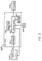
- the present invention is implemented at a review tool 300, as shown in Fig. 3, comprising an imager 310, preferably a CD-SEM such as the VeraSEMTM available from Applied Materials of Santa Clara, California.
- Review tool 300 further comprises a processor 320, which preferably performs the analysis disclosed herein electronically, and a monitor 330 for displaying results of the analyses of processor 320.
- Processor 320 can be in communication with a memory device 340, such as a semiconductor memory, and, a computer software-implemented database system 350 known as a "manufacturing execution system" (MES) conventionally used for storage of process information.
- MES manufacturing execution system
- Processor 320 is also in communication with previously-described photo cell 360 and etcher 370.
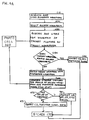
- Figure 4A is a flow chart illustrating the major steps of process control according to an embodiment of the present invention, implemented in conjunction with inspecting a feature (hereinafter called a "target feature") such as an etch mask formed on a semiconductor wafer W at photo cell 360.
- a feature hereinafter called a "target feature”
- the reference library is created, including reference CDs and waveforms in the form of SEM waveforms, and stored locally in inspection tool 300 or in MES 350.
- the stepper settings associated with each of the reference waveforms and the appropriate etch recipes are stored along with the waveforms. Profile images can also be stored, if desired by the user.
- the reference library is created only once for each layer to be inspected, such as when a series of process steps, such as photo cell 360, creates a "critical layer" that the user determines must be inspected.
- the golden waveform i.e., the waveform associated with the reference feature exhibiting optimal CD and/or other characteristics, is selected at step 420.
- Wafer W having features with unknown CD and other characteristics, is brought to imager 310 from photo cell 360, the target feature is imaged by imager 310 at step 430, and its waveform is stored as a target waveform.
- the target waveform is compared to the stored golden waveform. If the target waveform and golden waveform match within predetermined limits, the CD of the target feature is reported to the user, as by a display on monitor 330, along with a "matching score" indicating the amount of deviation of the target waveform from the golden waveform (see step 441).
- the results (i.e., the data) from the inspection are then sent to MES 350, and wafer W is sent to etcher 370 for further.
- the target waveform is compared to each of the reference waveforms in the library to identify the reference waveform most closely matching the target waveform (see step 450).
- the reported stepper settings are compared with those associated with the golden waveform at step 460 to determine the difference dEdF between the settings which produced the golden waveform and those which produced the target waveform; e.g., determine the difference between the focus setting associated with the golden waveform and the focus setting associated with the target waveform, and determine the difference between the exposure setting associated with the golden waveform and the exposure setting associated with the target waveform.
- This information is then sent to photo cell 360, where it is used to correct the stepper settings to minimize "drift" in the stepper, which would cause CD variations in subsequently processed wafers, by indicating the amount of adjustment to the stepper that is required, as well as which particular adjustments (i.e., focus, exposure, or both) should be made.
- dE and dF are compared to predetermined threshold values at step 470. If dE and dF are not greater than the predetermined threshold values, the CD and matching score of the target feature are reported at step 471, the data from the inspection is then sent to MES 350, and wafer W is sent to etcher 370. On the other hand, if dE and dF are greater than the predetermined threshold values, the CD and matching score of the target feature is reported at step 480, along with dE and dF and the associated etch recipe, which is sent to etcher 370 to adjust (or "update") the etch recipe to correct the CD deviation of the finished features on wafer W.
- the etch recipes can typically adjust the CD within a range of about 10% or less.
- steps 460 and 480 can be done manually or automatically.
- manual mode the user takes the reported process correction information and implements it manually at photo cell 360 and/or etcher 370. This allows expert input from the user to decide the need for process adjustment
- automated mode the process correction information is automatically fed to the stepper in photo cell 360 or to etcher 370 to effect the correction through recipe updating.
- This mode can be implemented by a software interface allowing communication between processor 320 and etcher 370, and between processor 320 and photo cell 360.
- the predetermined threshold test of step 470 can be used as a sensitivity filter to determine if updating is necessary.
- the automatic mode is advantageous because it enables quick feedback and consistency.
- the present methodology is carried out after a lot of wafers, such as about 25 wafers, is processed by photo cell 360.
- a number of wafers W from the lot are selected to be inspected, according to the user's preference. For example, when manufacturing microprocessors, 1-3 wafers are typically selected for inspection; however, when manufacturing memory devices such as DRAMs, only one wafer is typically inspected per lot.
- a number of sites on each selected wafer W are usually inspected by the present methodology (i.e., to be target features at step 430), such as about 9-17 sites per wafer W.
- the CDs of all the target features of the lot can be averaged, and the etch recipe associated with the average CD used to adjust the etch processing of the lot.
- the user can employ previously gathered process information to decide which sites on selected wafers W to inspect, and then decide which inspected feature's information to use to adjust photo cell 360.
- the user maps field to field CD variations across a number of wafers prior to inspection using the present methodology.
- This is a standard process control technique practiced by virtually all wafer fabricators. It indicates which areas of the wafer typically have small CD variations from the design value, and which areas of the wafer typically have a large CD variation.
- some wafer processing equipment e.g., photo cell 360
- Other equipment produces wafers having large CD variations near the center of the wafer and small CD variations in a band surrounding the center.
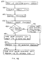
- the user identifies, at step 491, an area or areas of the wafers that exhibit the worst CD variation.
- Target features are then inspected at step 493 using the inventive methodology (e.g., steps 430 et seq. described above). Target features are selected such that fields in the worst part of the wafer, identified at step 491, are represented. If the field to field variation of the inspected features is smaller than the predetermined threshold (see step 494), dEdF associated with any one of the target features can be fed back to photo cell 360 for use in adjusting the processing of subsequent lots (step 495), since they are relatively close to each other.
- inventive methodology e.g., steps 430 et seq. described above.
- step 492 if the field to field variation of the inspected features is larger than the threshold value selected in step 492, dEdF associated with an inspected feature from the predetermined worst site from step 491 is fed back to photo cell 360 (see step 496). Thus, the worst CD variation is corrected in subsequent lots.
- the CDs of the inspected features are averaged, and at step 498, the etch recipe associated with the average CD is fed forward to etcher 370 to adjust (or "update") the etch recipe to correct the CD deviation of the features on the wafers in the inspected lot.
- this embodiment of the present invention allows the user to employ information, such as field to field CD variation maps, that they gather as a matter of course independently of implementing the present invention, to reduce lot to lot variation with minimal added cost and inspection time.
- FIG. 5 is a block diagram that illustrates an embodiment of the invention.
- processor 320 includes a bus 502 or other communication mechanism for communicating information, and a central processing unit 504 coupled with bus 502 for processing information.
- Processor 320 also includes a main memory 506, such as a random access memory (RAM) or other dynamic storage device, coupled to bus 502 for storing information and instructions to be executed by CPU 504.
- Main memory 506 also may be used for storing temporary variables or other intermediate information during execution of instructions to be executed by CPU 504.
- Processor 320 further includes a read only memory (ROM) 508 or other static storage device coupled to bus 502 for storing static information and instructions for CPU 504.
- ROM read only memory
- a storage device 510 such as a magnetic disk or optical disk, is provided and coupled to bus 502 for storing information and instructions. Storage device 510 may also serve as memory 340 in Fig. 3.
- Processor 320 may be coupled via bus 502 to monitor 330, such as a cathode ray tube (CRT), for displaying information to a computer user.
- monitor 330 such as a cathode ray tube (CRT)
- An input device 514 is coupled to bus 502 for communicating information and command selections to CPU 504.
- cursor control 516 is Another type of user input device
- cursor control 516 such as a mouse, a trackball, or cursor direction keys for communicating direction information and command selections to CPU 504 and for controlling cursor movement on monitor 330.
- Imager 310 (Fig. 3) inputs data representative of features of a semiconductor wafer under inspection, as discussed above, to bus 502. Such data may be stored in main memory 506 and/or storage device 510, and used by CPU 504 as it executes instructions. Imager 310 may also receive instructions via bus 502 from CPU 504.
- the invention is related to the use of processor 320 for inspecting features formed on the surface of a semiconductor wafer and controlling processing of the wafer.
- inspection of the surface of the wafer and wafer process control is provided by processor 320 in response to CPU 504 executing one or more sequences of one or more instructions contained in main memory 506.
- Such instructions may be read into main memory 506 from another computer-readable medium, such as storage device 510.
- Execution of the sequences of instructions contained in main memory 506 causes CPU 504 to perform the process steps described above.
- processors in a multi-processing arrangement may also be employed to execute the sequences of instructions contained in main memory 506.
- Non-volatile media include, for example, optical or magnetic disks, such as storage device 510.
- Volatile media include dynamic memory, such as main memory 506.
- Transmission media include coaxial cable, copper wire and fiber optics, including the wires that comprise bus 502. Transmission media can also take the form of acoustic or light waves, such as those generated during radio frequency (RF) and infrared (IR) data communications.
- RF radio frequency
- IR infrared
- Computer-readable media include, for example, a floppy disk, a flexible disk, hard disk, magnetic tape, any other magnetic medium, a CD-ROM, DVD, any other optical medium, punch cards, paper tape, any other physical medium with patterns of holes, a RAM, a PROM, and EPROM, a FLASH-EPROM, any other memory chip or cartridge, or any other medium from which a computer can read.
- Various forms of computer-readable media may be involved in carrying out one or more sequences of one or more instructions to CPU 504 for execution.
- the instructions may initially be borne on a magnetic disk of a remote computer.
- the remote computer can load the instructions into its dynamic memory and send the instructions over a telephone line using a modem.
- a modem local to processor 320 can receive the data on the telephone line and use an infrared transmitter to convert the data to an infrared signal.
- An infrared detector coupled to bus 502 can receive the data carried in the infrared signal and place the data on bus 502.
- Bus 502 carries the data to main memory 506, from which CPU 504 retrieves and executes the instructions.
- the instructions received by main memory 506 may optionally be stored on storage device 510 either before or after execution by CPU 504.
- the step of comparing the target waveform to the golden waveform (see Fig. 4A, step 440) and the step of matching the target waveform to one of the reference waveforms (step 450) comprise comparing only a selected portion of the target waveform and the reference/golden waveforms which represents a significant feature of the profile under inspection.
- Fig. 6A depicts a typical feature profile
- Fig. 6B shows the corresponding SEM waveform of the feature of Fig. 6A
- Fig. 6C is a graphical representation of the first derivative of the SEM waveform of Fig. 6B.
- portions 601a and 603a are the most important areas of the feature profile to be inspected, and correspond to segments 601b and 603b of the SEM waveform in Fig. 6B and segments 601c and 603c of the first derivative shown in Fig. 6C, it is advantageous to match segments 601c or 603c of the first derivatives of the target and reference waveforms.
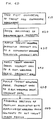
- the first derivative of the target and reference waveforms are taken (step 610), and divided into segments at step 620, such as segments 601c, 602c and 603c in Fig. 6C. Then, each of segments 601c, 602c and 603c of the derivative of the target waveform is separately matched to a corresponding segment of the derivative of a reference waveform (see steps 630, 640, 650), which is associated with a portion of a known profile (e.g., portion 601a, 602a, 603a of Fig. 6A).
- the profile of the target feature is predicted by assembling "building blocks" of matching segments (step 660).
- An examination of the predicted profile will indicate what part or parts of the profile deviate from design standards, and such information can be used by one skilled in the art to trace photolithographic processing problems, such as focus and exposure problems.
- the step of comparing the target waveform to the golden waveform (step 440) and the step of matching the target waveform to one of the reference waveforms (step 450) comprise employing an algorithm to "fit a curve" to the target and reference SEM waveforms such as depicted in Fig. 6B; that is, to obtain a mathematical function or "formula" representative of the shape of each of the waveforms. Then, corresponding significant elements of the mathematical functions representative of the target and reference waveforms are compared to determine which reference image most closely matches the target image.
- the reference waveform whose values of x, a and b most closely match the x, a and b values of the target waveform is the reference waveform that most closely matches the target waveform.
- the step of comparing the target waveform to the golden waveform (step 440) and the step of matching the target waveform to one of the reference waveforms (step 450) comprise using the target and reference waveforms to generate images of the target feature and the reference features, and then comparing the generated images.
- SEM waveforms as illustrated in Fig. 6B are manipulated using conventional computer graphics techniques to generate images as shown in Fig. 6A.
- the generated images are then matched, as by well-known pattern recognition techniques such as boundary analysis and grey-scale analysis.
- the inventive process control technique enables lot to lot CD variations to be reduced without significantly reducing production throughput by using data gathered during the inspection process to adjust photolithography and etch process parameters.
- the inventive methodology determines an inspected feature's stepper settings and optimal etch recipe by comparing its SEM waveform with the waveforms of a library of reference features obtained by forming a pie-production FEM. Therefore, the present invention is especially useful during the start-up and ramp-up of a production line.
- the present invention is applicable to the manufacture of various types of semiconductor devices, particularly high density semiconductor devices having a design rule of about 0.18 ⁇ and under.
Landscapes
- Physics & Mathematics (AREA)
- General Physics & Mathematics (AREA)
- Exposure And Positioning Against Photoresist Photosensitive Materials (AREA)
- Testing Or Measuring Of Semiconductors Or The Like (AREA)
- Exposure Of Semiconductors, Excluding Electron Or Ion Beam Exposure (AREA)
Applications Claiming Priority (2)
| Application Number | Priority Date | Filing Date | Title |
|---|---|---|---|
| US34280599A | 1999-06-29 | 1999-06-29 | |
| US342805 | 1999-06-29 |
Publications (2)
| Publication Number | Publication Date |
|---|---|
| EP1065567A2 true EP1065567A2 (de) | 2001-01-03 |
| EP1065567A3 EP1065567A3 (de) | 2001-05-16 |
Family
ID=23343348
Family Applications (1)
| Application Number | Title | Priority Date | Filing Date |
|---|---|---|---|
| EP00113788A Withdrawn EP1065567A3 (de) | 1999-06-29 | 2000-06-29 | Integrierte Kontrolle einer kritischen Dimension |
Country Status (4)
| Country | Link |
|---|---|
| US (3) | US6388253B1 (de) |
| EP (1) | EP1065567A3 (de) |
| JP (1) | JP2001143982A (de) |
| KR (1) | KR100702741B1 (de) |
Cited By (32)
| Publication number | Priority date | Publication date | Assignee | Title |
|---|---|---|---|---|
| EP1184725A1 (de) * | 2000-09-04 | 2002-03-06 | Infineon Technologies SC300 GmbH & Co. KG | Verfahren zur Einstellung eines lithographischen Gerätes |
| DE10037243A1 (de) * | 2000-07-31 | 2002-03-07 | Infineon Technologies Ag | Regelsystem für photolithographische Prozesse |
| US6689519B2 (en) | 2000-05-04 | 2004-02-10 | Kla-Tencor Technologies Corp. | Methods and systems for lithography process control |
| WO2003003123A3 (en) * | 2001-06-28 | 2004-03-18 | Advanced Micro Devices Inc | Critical dimension monitoring from latent image |
| US6956659B2 (en) | 2001-05-22 | 2005-10-18 | Nikon Precision Inc. | Measurement of critical dimensions of etched features |
| US6974653B2 (en) | 2002-04-19 | 2005-12-13 | Nikon Precision Inc. | Methods for critical dimension and focus mapping using critical dimension test marks |
| US7027143B1 (en) | 2002-10-15 | 2006-04-11 | Kla-Tencor Technologies Corp. | Methods and systems for inspecting reticles using aerial imaging at off-stepper wavelengths |
| WO2004097528A3 (en) * | 2003-04-29 | 2006-07-20 | Koninkl Philips Electronics Nv | System and method for characterizing lithography effects on a wafer |
| US7123356B1 (en) | 2002-10-15 | 2006-10-17 | Kla-Tencor Technologies Corp. | Methods and systems for inspecting reticles using aerial imaging and die-to-database detection |
| US7379175B1 (en) | 2002-10-15 | 2008-05-27 | Kla-Tencor Technologies Corp. | Methods and systems for reticle inspection and defect review using aerial imaging |
| US7570796B2 (en) | 2005-11-18 | 2009-08-04 | Kla-Tencor Technologies Corp. | Methods and systems for utilizing design data in combination with inspection data |
| US7646906B2 (en) | 2004-01-29 | 2010-01-12 | Kla-Tencor Technologies Corp. | Computer-implemented methods for detecting defects in reticle design data |
| US7676077B2 (en) | 2005-11-18 | 2010-03-09 | Kla-Tencor Technologies Corp. | Methods and systems for utilizing design data in combination with inspection data |
| US7689966B2 (en) | 2004-09-14 | 2010-03-30 | Kla-Tencor Technologies Corp. | Methods, systems, and carrier media for evaluating reticle layout data |
| US7711514B2 (en) | 2007-08-10 | 2010-05-04 | Kla-Tencor Technologies Corp. | Computer-implemented methods, carrier media, and systems for generating a metrology sampling plan |
| US7738093B2 (en) | 2007-05-07 | 2010-06-15 | Kla-Tencor Corp. | Methods for detecting and classifying defects on a reticle |
| US7769225B2 (en) | 2005-08-02 | 2010-08-03 | Kla-Tencor Technologies Corp. | Methods and systems for detecting defects in a reticle design pattern |
| US7796804B2 (en) | 2007-07-20 | 2010-09-14 | Kla-Tencor Corp. | Methods for generating a standard reference die for use in a die to standard reference die inspection and methods for inspecting a wafer |
| US7877722B2 (en) | 2006-12-19 | 2011-01-25 | Kla-Tencor Corp. | Systems and methods for creating inspection recipes |
| US7962863B2 (en) | 2007-05-07 | 2011-06-14 | Kla-Tencor Corp. | Computer-implemented methods, systems, and computer-readable media for determining a model for predicting printability of reticle features on a wafer |
| US7975245B2 (en) | 2007-08-20 | 2011-07-05 | Kla-Tencor Corp. | Computer-implemented methods for determining if actual defects are potentially systematic defects or potentially random defects |
| US8041103B2 (en) | 2005-11-18 | 2011-10-18 | Kla-Tencor Technologies Corp. | Methods and systems for determining a position of inspection data in design data space |
| US8112241B2 (en) | 2009-03-13 | 2012-02-07 | Kla-Tencor Corp. | Methods and systems for generating an inspection process for a wafer |
| US8139844B2 (en) | 2008-04-14 | 2012-03-20 | Kla-Tencor Corp. | Methods and systems for determining a defect criticality index for defects on wafers |
| US8194968B2 (en) | 2007-01-05 | 2012-06-05 | Kla-Tencor Corp. | Methods and systems for using electrical information for a device being fabricated on a wafer to perform one or more defect-related functions |
| US8204297B1 (en) | 2009-02-27 | 2012-06-19 | Kla-Tencor Corp. | Methods and systems for classifying defects detected on a reticle |
| US8213704B2 (en) | 2007-05-09 | 2012-07-03 | Kla-Tencor Corp. | Methods and systems for detecting defects in a reticle design pattern |
| US9053527B2 (en) | 2013-01-02 | 2015-06-09 | Kla-Tencor Corp. | Detecting defects on a wafer |
| US9087367B2 (en) | 2011-09-13 | 2015-07-21 | Kla-Tencor Corp. | Determining design coordinates for wafer defects |
| US9092846B2 (en) | 2013-02-01 | 2015-07-28 | Kla-Tencor Corp. | Detecting defects on a wafer using defect-specific and multi-channel information |
| US9659670B2 (en) | 2008-07-28 | 2017-05-23 | Kla-Tencor Corp. | Computer-implemented methods, computer-readable media, and systems for classifying defects detected in a memory device area on a wafer |
| US9865512B2 (en) | 2013-04-08 | 2018-01-09 | Kla-Tencor Corp. | Dynamic design attributes for wafer inspection |
Families Citing this family (185)
| Publication number | Priority date | Publication date | Assignee | Title |
|---|---|---|---|---|
| US7069101B1 (en) * | 1999-07-29 | 2006-06-27 | Applied Materials, Inc. | Computer integrated manufacturing techniques |
| US6560504B1 (en) * | 1999-09-29 | 2003-05-06 | Advanced Micro Devices, Inc. | Use of contamination-free manufacturing data in fault detection and classification as well as in run-to-run control |
| US6873087B1 (en) * | 1999-10-29 | 2005-03-29 | Board Of Regents, The University Of Texas System | High precision orientation alignment and gap control stages for imprint lithography processes |
| US6640151B1 (en) | 1999-12-22 | 2003-10-28 | Applied Materials, Inc. | Multi-tool control system, method and medium |
| US6650957B1 (en) * | 2000-01-03 | 2003-11-18 | Advanced Micro Devices, Inc. | Method and apparatus for run-to-run control of deposition process |
| US6567717B2 (en) * | 2000-01-19 | 2003-05-20 | Advanced Micro Devices, Inc. | Feed-forward control of TCI doping for improving mass-production-wise, statistical distribution of critical performance parameters in semiconductor devices |
| US6694275B1 (en) * | 2000-06-02 | 2004-02-17 | Timbre Technologies, Inc. | Profiler business model |
| SG142150A1 (en) * | 2000-07-16 | 2008-05-28 | Univ Texas | High-resolution overlay alignment systems for imprint lithography |
| KR100827741B1 (ko) | 2000-07-17 | 2008-05-07 | 보드 오브 리전츠, 더 유니버시티 오브 텍사스 시스템 | 임프린트 리소그래피 공정을 위한 자동 유체 분배 방법 및시스템 |
| US6625512B1 (en) * | 2000-07-25 | 2003-09-23 | Advanced Micro Devices, Inc. | Method and apparatus for performing final critical dimension control |
| JP2004505273A (ja) * | 2000-08-01 | 2004-02-19 | ボード・オブ・リージエンツ,ザ・ユニバーシテイ・オブ・テキサス・システム | 転写リソグラフィのための透明テンプレートと基板の間のギャップおよび配向を高精度でセンシングするための方法 |
| US6708074B1 (en) | 2000-08-11 | 2004-03-16 | Applied Materials, Inc. | Generic interface builder |
| US6625513B1 (en) * | 2000-08-15 | 2003-09-23 | Applied Materials, Inc. | Run-to-run control over semiconductor processing tool based upon mirror image target |
| US6694284B1 (en) | 2000-09-20 | 2004-02-17 | Kla-Tencor Technologies Corp. | Methods and systems for determining at least four properties of a specimen |
| US7130029B2 (en) | 2000-09-20 | 2006-10-31 | Kla-Tencor Technologies Corp. | Methods and systems for determining an adhesion characteristic and a thickness of a specimen |
| US6919957B2 (en) | 2000-09-20 | 2005-07-19 | Kla-Tencor Technologies Corp. | Methods and systems for determining a critical dimension, a presence of defects, and a thin film characteristic of a specimen |
| US6891627B1 (en) | 2000-09-20 | 2005-05-10 | Kla-Tencor Technologies Corp. | Methods and systems for determining a critical dimension and overlay of a specimen |
| US6673637B2 (en) | 2000-09-20 | 2004-01-06 | Kla-Tencor Technologies | Methods and systems for determining a presence of macro defects and overlay of a specimen |
| US6782337B2 (en) | 2000-09-20 | 2004-08-24 | Kla-Tencor Technologies Corp. | Methods and systems for determining a critical dimension an a presence of defects on a specimen |
| US6633831B2 (en) | 2000-09-20 | 2003-10-14 | Kla Tencor Technologies | Methods and systems for determining a critical dimension and a thin film characteristic of a specimen |
| US7106425B1 (en) | 2000-09-20 | 2006-09-12 | Kla-Tencor Technologies Corp. | Methods and systems for determining a presence of defects and a thin film characteristic of a specimen |
| US7349090B2 (en) | 2000-09-20 | 2008-03-25 | Kla-Tencor Technologies Corp. | Methods and systems for determining a property of a specimen prior to, during, or subsequent to lithography |
| US6812045B1 (en) | 2000-09-20 | 2004-11-02 | Kla-Tencor, Inc. | Methods and systems for determining a characteristic of a specimen prior to, during, or subsequent to ion implantation |
| CN100365507C (zh) * | 2000-10-12 | 2008-01-30 | 德克萨斯州大学系统董事会 | 用于室温下低压微刻痕和毫微刻痕光刻的模板 |
| US7188142B2 (en) | 2000-11-30 | 2007-03-06 | Applied Materials, Inc. | Dynamic subject information generation in message services of distributed object systems in a semiconductor assembly line facility |
| IL140179A (en) * | 2000-12-07 | 2004-09-27 | Nova Measuring Instr Ltd | Method and system for measuring in patterned structures |
| US7029484B2 (en) * | 2001-01-04 | 2006-04-18 | Biocurv Medical Instruments, Inc. | Tongue cleaning device |
| US6632692B1 (en) * | 2001-01-11 | 2003-10-14 | Advanced Micro Devices, Inc. | Automated method of controlling critical dimensions of features by controlling stepper exposure dose, and system for accomplishing same |
| US6569692B1 (en) | 2001-02-02 | 2003-05-27 | Advanced Micro Devices, Inc. | Automated method of controlling photoresist develop time to control critical dimensions, and system for accomplishing same |
| US20020128735A1 (en) * | 2001-03-08 | 2002-09-12 | Hawkins Parris C.M. | Dynamic and extensible task guide |
| US6901340B1 (en) * | 2001-04-02 | 2005-05-31 | Advanced Micro Devices, Inc. | Method and apparatus for distinguishing between sources of process variation |
| US20020152046A1 (en) * | 2001-04-13 | 2002-10-17 | Velichko Sergey A. | Concurrent control of semiconductor parametric testing |
| US6501534B1 (en) * | 2001-04-30 | 2002-12-31 | Advanced Micro Devices, Inc. | Automated periodic focus and exposure calibration of a lithography stepper |
| US7052575B1 (en) * | 2001-04-30 | 2006-05-30 | Advanced Micro Devices, Inc. | System and method for active control of etch process |
| US6964793B2 (en) * | 2002-05-16 | 2005-11-15 | Board Of Regents, The University Of Texas System | Method for fabricating nanoscale patterns in light curable compositions using an electric field |
| US7337088B2 (en) * | 2001-05-23 | 2008-02-26 | Micron Technology, Inc. | Intelligent measurement modular semiconductor parametric test system |
| US7201936B2 (en) | 2001-06-19 | 2007-04-10 | Applied Materials, Inc. | Method of feedback control of sub-atmospheric chemical vapor deposition processes |
| US7047099B2 (en) | 2001-06-19 | 2006-05-16 | Applied Materials Inc. | Integrating tool, module, and fab level control |
| US6537833B1 (en) * | 2001-06-19 | 2003-03-25 | Advanced Micro Devices, Inc. | Method and apparatus for characterizing an interconnect structure profile using scatterometry measurements |
| US7082345B2 (en) | 2001-06-19 | 2006-07-25 | Applied Materials, Inc. | Method, system and medium for process control for the matching of tools, chambers and/or other semiconductor-related entities |
| US7698012B2 (en) | 2001-06-19 | 2010-04-13 | Applied Materials, Inc. | Dynamic metrology schemes and sampling schemes for advanced process control in semiconductor processing |
| US7160739B2 (en) | 2001-06-19 | 2007-01-09 | Applied Materials, Inc. | Feedback control of a chemical mechanical polishing device providing manipulation of removal rate profiles |
| US6913938B2 (en) | 2001-06-19 | 2005-07-05 | Applied Materials, Inc. | Feedback control of plasma-enhanced chemical vapor deposition processes |
| US7101799B2 (en) * | 2001-06-19 | 2006-09-05 | Applied Materials, Inc. | Feedforward and feedback control for conditioning of chemical mechanical polishing pad |
| US6910947B2 (en) | 2001-06-19 | 2005-06-28 | Applied Materials, Inc. | Control of chemical mechanical polishing pad conditioner directional velocity to improve pad life |
| US6440759B1 (en) * | 2001-06-29 | 2002-08-27 | Infineon Technologies Ag | Method of measuring combined critical dimension and overlay in single step |
| US7479633B2 (en) * | 2001-07-10 | 2009-01-20 | International Business Machines Corporation | Methodology for critical dimension metrology using stepper focus monitor information |
| US7337019B2 (en) | 2001-07-16 | 2008-02-26 | Applied Materials, Inc. | Integration of fault detection with run-to-run control |
| US6950716B2 (en) | 2001-08-13 | 2005-09-27 | Applied Materials, Inc. | Dynamic control of wafer processing paths in semiconductor manufacturing processes |
| US6984198B2 (en) | 2001-08-14 | 2006-01-10 | Applied Materials, Inc. | Experiment management system, method and medium |
| AU2002341677A1 (en) * | 2001-09-18 | 2003-04-01 | Applied Materials, Inc. | Integrated equipment set for forming an interconnect on a substrate |
| JP3817464B2 (ja) * | 2001-11-13 | 2006-09-06 | 株式会社日立ハイテクノロジーズ | 微細パターンの3次元形状測定システム、及び3次元形状測定方法 |
| US6708075B2 (en) * | 2001-11-16 | 2004-03-16 | Advanced Micro Devices | Method and apparatus for utilizing integrated metrology data as feed-forward data |
| US20030220708A1 (en) * | 2001-11-28 | 2003-11-27 | Applied Materials, Inc. | Integrated equipment set for forming shallow trench isolation regions |
| US6708129B1 (en) * | 2001-12-13 | 2004-03-16 | Advanced Micro Devices, Inc. | Method and apparatus for wafer-to-wafer control with partial measurement data |
| US6960416B2 (en) * | 2002-03-01 | 2005-11-01 | Applied Materials, Inc. | Method and apparatus for controlling etch processes during fabrication of semiconductor devices |
| US7225047B2 (en) | 2002-03-19 | 2007-05-29 | Applied Materials, Inc. | Method, system and medium for controlling semiconductor wafer processes using critical dimension measurements |
| US20030199112A1 (en) | 2002-03-22 | 2003-10-23 | Applied Materials, Inc. | Copper wiring module control |
| US6792328B2 (en) * | 2002-03-29 | 2004-09-14 | Timbre Technologies, Inc. | Metrology diffraction signal adaptation for tool-to-tool matching |
| US7162386B2 (en) * | 2002-04-25 | 2007-01-09 | Micron Technology, Inc. | Dynamically adaptable semiconductor parametric testing |
| US6672716B2 (en) * | 2002-04-29 | 2004-01-06 | Xerox Corporation | Multiple portion solid ink stick |
| US7037639B2 (en) * | 2002-05-01 | 2006-05-02 | Molecular Imprints, Inc. | Methods of manufacturing a lithography template |
| US6708574B2 (en) * | 2002-05-24 | 2004-03-23 | Agere Systems, Inc. | Abnormal photoresist line/space profile detection through signal processing of metrology waveform |
| US20040007325A1 (en) * | 2002-06-11 | 2004-01-15 | Applied Materials, Inc. | Integrated equipment set for forming a low K dielectric interconnect on a substrate |
| US20040206621A1 (en) * | 2002-06-11 | 2004-10-21 | Hongwen Li | Integrated equipment set for forming a low K dielectric interconnect on a substrate |
| US6924088B2 (en) * | 2002-06-20 | 2005-08-02 | Applied Materials, Inc. | Method and system for realtime CD microloading control |
| US20030235787A1 (en) * | 2002-06-24 | 2003-12-25 | Watts Michael P.C. | Low viscosity high resolution patterning material |
| US6926929B2 (en) | 2002-07-09 | 2005-08-09 | Molecular Imprints, Inc. | System and method for dispensing liquids |
| US7077992B2 (en) | 2002-07-11 | 2006-07-18 | Molecular Imprints, Inc. | Step and repeat imprint lithography processes |
| US6900881B2 (en) | 2002-07-11 | 2005-05-31 | Molecular Imprints, Inc. | Step and repeat imprint lithography systems |
| US6932934B2 (en) | 2002-07-11 | 2005-08-23 | Molecular Imprints, Inc. | Formation of discontinuous films during an imprint lithography process |
| US6908861B2 (en) * | 2002-07-11 | 2005-06-21 | Molecular Imprints, Inc. | Method for imprint lithography using an electric field |
| US7019819B2 (en) | 2002-11-13 | 2006-03-28 | Molecular Imprints, Inc. | Chucking system for modulating shapes of substrates |
| US7668702B2 (en) * | 2002-07-19 | 2010-02-23 | Applied Materials, Inc. | Method, system and medium for controlling manufacturing process using adaptive models based on empirical data |
| US7070405B2 (en) * | 2002-08-01 | 2006-07-04 | Molecular Imprints, Inc. | Alignment systems for imprint lithography |
| US7027156B2 (en) | 2002-08-01 | 2006-04-11 | Molecular Imprints, Inc. | Scatterometry alignment for imprint lithography |
| US6916584B2 (en) | 2002-08-01 | 2005-07-12 | Molecular Imprints, Inc. | Alignment methods for imprint lithography |
| KR20050026099A (ko) | 2002-08-01 | 2005-03-14 | 어플라이드 머티어리얼즈 인코포레이티드 | 고급 처리 제어 시스템 내의 부정확한 계측 데이터의 취급방법, 시스템 및 매체 |
| US7071088B2 (en) * | 2002-08-23 | 2006-07-04 | Molecular Imprints, Inc. | Method for fabricating bulbous-shaped vias |
| US6810296B2 (en) * | 2002-09-25 | 2004-10-26 | Advanced Micro Devices, Inc. | Correlating an inline parameter to a device operation parameter |
| US8349241B2 (en) | 2002-10-04 | 2013-01-08 | Molecular Imprints, Inc. | Method to arrange features on a substrate to replicate features having minimal dimensional variability |
| DE10250893B4 (de) * | 2002-10-31 | 2008-04-03 | Advanced Micro Devices, Inc., Sunnyvale | Verfahren und Vorrichtung zum Bestimmen der Abmessung eines Strukturelements durch Variieren eines die Auflösung bestimmenden Parameters |
| US7265382B2 (en) * | 2002-11-12 | 2007-09-04 | Applied Materials, Inc. | Method and apparatus employing integrated metrology for improved dielectric etch efficiency |
| US6929762B2 (en) | 2002-11-13 | 2005-08-16 | Molecular Imprints, Inc. | Method of reducing pattern distortions during imprint lithography processes |
| US6980282B2 (en) * | 2002-12-11 | 2005-12-27 | Molecular Imprints, Inc. | Method for modulating shapes of substrates |
| WO2004046835A2 (en) | 2002-11-15 | 2004-06-03 | Applied Materials, Inc. | Method, system and medium for controlling manufacture process having multivariate input parameters |
| US6871558B2 (en) * | 2002-12-12 | 2005-03-29 | Molecular Imprints, Inc. | Method for determining characteristics of substrate employing fluid geometries |
| US7333871B2 (en) | 2003-01-21 | 2008-02-19 | Applied Materials, Inc. | Automated design and execution of experiments with integrated model creation for semiconductor manufacturing tools |
| US7452574B2 (en) * | 2003-02-27 | 2008-11-18 | Molecular Imprints, Inc. | Method to reduce adhesion between a polymerizable layer and a substrate employing a fluorine-containing layer |
| US7081369B2 (en) * | 2003-02-28 | 2006-07-25 | Intel Corporation | Forming a semiconductor device feature using acquired parameters |
| US7122079B2 (en) | 2004-02-27 | 2006-10-17 | Molecular Imprints, Inc. | Composition for an etching mask comprising a silicon-containing material |
| US7179396B2 (en) * | 2003-03-25 | 2007-02-20 | Molecular Imprints, Inc. | Positive tone bi-layer imprint lithography method |
| US6766214B1 (en) * | 2003-04-03 | 2004-07-20 | Advanced Micro Devices, Inc. | Adjusting a sampling rate based on state estimation results |
| US8257546B2 (en) * | 2003-04-11 | 2012-09-04 | Applied Materials, Inc. | Method and system for monitoring an etch process |
| US20040200574A1 (en) * | 2003-04-11 | 2004-10-14 | Applied Materials, Inc. | Method for controlling a process for fabricating integrated devices |
| US7010451B2 (en) * | 2003-04-17 | 2006-03-07 | Micron Technology, Inc. | Dynamic creation and modification of wafer test maps during wafer testing |
| US6931617B2 (en) * | 2003-04-21 | 2005-08-16 | Synopsys, Inc. | Mask cost driven logic optimization and synthesis |
| US7396475B2 (en) * | 2003-04-25 | 2008-07-08 | Molecular Imprints, Inc. | Method of forming stepped structures employing imprint lithography |
| US6808942B1 (en) * | 2003-05-23 | 2004-10-26 | Texas Instruments Incorporated | Method for controlling a critical dimension (CD) in an etch process |
| US7135259B2 (en) | 2003-05-28 | 2006-11-14 | Taiwan Semiconductor Manufacturing Co., Ltd. | Scatterometric method of monitoring hot plate temperature and facilitating critical dimension control |
| US7205228B2 (en) | 2003-06-03 | 2007-04-17 | Applied Materials, Inc. | Selective metal encapsulation schemes |
| US7157036B2 (en) | 2003-06-17 | 2007-01-02 | Molecular Imprints, Inc | Method to reduce adhesion between a conformable region and a pattern of a mold |
| US9002497B2 (en) * | 2003-07-03 | 2015-04-07 | Kla-Tencor Technologies Corp. | Methods and systems for inspection of wafers and reticles using designer intent data |
| JP2005038976A (ja) * | 2003-07-18 | 2005-02-10 | Hitachi High-Technologies Corp | 最適エッチングパラメタ自動設定システムおよびエッチング出来ばえ評価システム |
| US7354332B2 (en) | 2003-08-04 | 2008-04-08 | Applied Materials, Inc. | Technique for process-qualifying a semiconductor manufacturing tool using metrology data |
| US7482178B2 (en) * | 2003-08-06 | 2009-01-27 | Applied Materials, Inc. | Chamber stability monitoring using an integrated metrology tool |
| US6829056B1 (en) | 2003-08-21 | 2004-12-07 | Michael Barnes | Monitoring dimensions of features at different locations in the processing of substrates |
| US20050064714A1 (en) * | 2003-09-19 | 2005-03-24 | Applied Materials, Inc. | Method for controlling critical dimensions during an etch process |
| US6911399B2 (en) * | 2003-09-19 | 2005-06-28 | Applied Materials, Inc. | Method of controlling critical dimension microloading of photoresist trimming process by selective sidewall polymer deposition |
| US7136150B2 (en) | 2003-09-25 | 2006-11-14 | Molecular Imprints, Inc. | Imprint lithography template having opaque alignment marks |
| US8211214B2 (en) * | 2003-10-02 | 2012-07-03 | Molecular Imprints, Inc. | Single phase fluid imprint lithography method |
| US7090716B2 (en) * | 2003-10-02 | 2006-08-15 | Molecular Imprints, Inc. | Single phase fluid imprint lithography method |
| JP4671594B2 (ja) * | 2003-10-08 | 2011-04-20 | 株式会社日立ハイテクノロジーズ | データ収集管理方法およびそのシステム |
| US7094613B2 (en) * | 2003-10-21 | 2006-08-22 | Applied Materials, Inc. | Method for controlling accuracy and repeatability of an etch process |
| ATE476687T1 (de) | 2003-12-19 | 2010-08-15 | Ibm | Differentielle metrologie für kritische abmessung und überlagerung |
| US7250309B2 (en) * | 2004-01-09 | 2007-07-31 | Applied Materials, Inc. | Integrated phase angle and optical critical dimension measurement metrology for feed forward and feedback process control |
| US7356377B2 (en) | 2004-01-29 | 2008-04-08 | Applied Materials, Inc. | System, method, and medium for monitoring performance of an advanced process control system |
| US7306746B2 (en) * | 2004-01-30 | 2007-12-11 | Taiwan Semiconductor Manufacturing Co. Ltd. | Critical dimension control in a semiconductor fabrication process |
| US7198964B1 (en) | 2004-02-03 | 2007-04-03 | Advanced Micro Devices, Inc. | Method and apparatus for detecting faults using principal component analysis parameter groupings |
| US8076386B2 (en) | 2004-02-23 | 2011-12-13 | Molecular Imprints, Inc. | Materials for imprint lithography |
| US7906180B2 (en) | 2004-02-27 | 2011-03-15 | Molecular Imprints, Inc. | Composition for an etching mask comprising a silicon-containing material |
| US6961626B1 (en) | 2004-05-28 | 2005-11-01 | Applied Materials, Inc | Dynamic offset and feedback threshold |
| US7096085B2 (en) | 2004-05-28 | 2006-08-22 | Applied Materials | Process control by distinguishing a white noise component of a process variance |
| US7065423B2 (en) * | 2004-07-08 | 2006-06-20 | Timbre Technologies, Inc. | Optical metrology model optimization for process control |
| US7150673B2 (en) * | 2004-07-09 | 2006-12-19 | Ebara Corporation | Method for estimating polishing profile or polishing amount, polishing method and polishing apparatus |
| US7250373B2 (en) * | 2004-08-27 | 2007-07-31 | Applied Materials, Inc. | Method and apparatus for etching material layers with high uniformity of a lateral etch rate across a substrate |
| US7301645B2 (en) * | 2004-08-31 | 2007-11-27 | Taiwan Semiconductor Manufacturing Co., Ltd. | In-situ critical dimension measurement |
| US20060135049A1 (en) * | 2004-12-16 | 2006-06-22 | Petersen John G | Millwork sanding sponge |
| KR100588914B1 (ko) | 2004-12-22 | 2006-06-09 | 동부일렉트로닉스 주식회사 | 웨이퍼 상의 트랜지스터의 균일한 전기적 특성을 위한노광방법 |
| US20060145398A1 (en) * | 2004-12-30 | 2006-07-06 | Board Of Regents, The University Of Texas System | Release layer comprising diamond-like carbon (DLC) or doped DLC with tunable composition for imprint lithography templates and contact masks |
| US7601272B2 (en) * | 2005-01-08 | 2009-10-13 | Applied Materials, Inc. | Method and apparatus for integrating metrology with etch processing |
| US20060154388A1 (en) * | 2005-01-08 | 2006-07-13 | Richard Lewington | Integrated metrology chamber for transparent substrates |
| JP2006228843A (ja) | 2005-02-16 | 2006-08-31 | Renesas Technology Corp | 半導体デバイスのプロセス制御方法および製造方法 |
| US7856138B2 (en) * | 2005-02-24 | 2010-12-21 | Applied Materials Israel, Ltd. | System, method and computer software product for inspecting charged particle responsive resist |
| US7142940B2 (en) * | 2005-03-14 | 2006-11-28 | Umci Ltd. | Method of processing semiconductor wafer |
| JP4262690B2 (ja) * | 2005-03-16 | 2009-05-13 | 株式会社日立ハイテクノロジーズ | 形状測定装置および形状測定方法 |
| US7588946B2 (en) * | 2005-07-25 | 2009-09-15 | Taiwan Semiconductor Manufacturing Company, Ltd. | Controlling system for gate formation of semiconductor devices |
| US7566900B2 (en) * | 2005-08-31 | 2009-07-28 | Applied Materials, Inc. | Integrated metrology tools for monitoring and controlling large area substrate processing chambers |
| US7962113B2 (en) * | 2005-10-31 | 2011-06-14 | Silicon Laboratories Inc. | Receiver with multi-tone wideband I/Q mismatch calibration and method therefor |
| US7803308B2 (en) * | 2005-12-01 | 2010-09-28 | Molecular Imprints, Inc. | Technique for separating a mold from solidified imprinting material |
| US7906058B2 (en) * | 2005-12-01 | 2011-03-15 | Molecular Imprints, Inc. | Bifurcated contact printing technique |
| US7670530B2 (en) * | 2006-01-20 | 2010-03-02 | Molecular Imprints, Inc. | Patterning substrates employing multiple chucks |
| MY144847A (en) | 2005-12-08 | 2011-11-30 | Molecular Imprints Inc | Method and system for double-sided patterning of substrates |
| US7631286B2 (en) * | 2005-12-30 | 2009-12-08 | Wafertech Llc | Automated metrology recipe generation |
| US7305320B2 (en) * | 2006-02-15 | 2007-12-04 | International Business Machines Corporation | Metrology tool recipe validator using best known methods |
| US7474420B2 (en) * | 2006-03-30 | 2009-01-06 | Timbre Technologies, Inc. | In-die optical metrology |
| US8850980B2 (en) | 2006-04-03 | 2014-10-07 | Canon Nanotechnologies, Inc. | Tessellated patterns in imprint lithography |
| US7780893B2 (en) * | 2006-04-03 | 2010-08-24 | Molecular Imprints, Inc. | Method of concurrently patterning a substrate having a plurality of fields and a plurality of alignment marks |
| US7802978B2 (en) | 2006-04-03 | 2010-09-28 | Molecular Imprints, Inc. | Imprinting of partial fields at the edge of the wafer |
| US8142850B2 (en) | 2006-04-03 | 2012-03-27 | Molecular Imprints, Inc. | Patterning a plurality of fields on a substrate to compensate for differing evaporation times |
| US8012395B2 (en) * | 2006-04-18 | 2011-09-06 | Molecular Imprints, Inc. | Template having alignment marks formed of contrast material |
| US7547398B2 (en) * | 2006-04-18 | 2009-06-16 | Molecular Imprints, Inc. | Self-aligned process for fabricating imprint templates containing variously etched features |
| US7875851B1 (en) * | 2006-05-01 | 2011-01-25 | Advanced Micro Devices, Inc. | Advanced process control framework using two-dimensional image analysis |
| US7774082B2 (en) | 2006-10-05 | 2010-08-10 | Tokyo Electron Limited | Substrate processing method and storage medium having program stored therein |
| JP5165878B2 (ja) * | 2006-10-20 | 2013-03-21 | 東京エレクトロン株式会社 | 基板処理装置の制御装置、制御方法および制御プログラムを記憶した記憶媒体 |
| JP4981410B2 (ja) * | 2006-10-31 | 2012-07-18 | 株式会社日立ハイテクノロジーズ | 走査型電子顕微鏡、走査型電子顕微鏡を用いたパターンの複合検査方法、および走査型電子顕微鏡の制御装置 |
| US7875198B2 (en) * | 2006-11-06 | 2011-01-25 | Macronix International Co., Ltd. | Method of deriving etching correction values for patterns of photomask and method of fabricating photomask |
| US7671273B2 (en) | 2007-10-09 | 2010-03-02 | International Business Machines Corporation | Method and apparatus for facilitating signal transmission using differential transmission lines |
| TW201025473A (en) * | 2008-12-30 | 2010-07-01 | Princeton Technology Corp | Product verification system |
| US8775101B2 (en) | 2009-02-13 | 2014-07-08 | Kla-Tencor Corp. | Detecting defects on a wafer |
| US8221635B2 (en) * | 2009-03-03 | 2012-07-17 | Raytheon Company | Process for multiple platings and fine etch accuracy on the same printed wiring board |
| US8767179B2 (en) * | 2009-12-15 | 2014-07-01 | Micron Technology, Inc. | Imaging methods in scanning photolithography and a scanning photolithography device used in printing an image of a reticle onto a photosensitive substrate |
| CN102194668B (zh) * | 2010-03-15 | 2013-05-01 | 中芯国际集成电路制造(上海)有限公司 | 一种在半导体器件中形成开口结构的方法 |
| US8781781B2 (en) | 2010-07-30 | 2014-07-15 | Kla-Tencor Corp. | Dynamic care areas |
| CN102593041B (zh) * | 2011-01-07 | 2015-07-15 | 上海华虹宏力半导体制造有限公司 | 一种刻蚀方法 |
| US9170211B2 (en) | 2011-03-25 | 2015-10-27 | Kla-Tencor Corp. | Design-based inspection using repeating structures |
| US8810785B2 (en) * | 2011-08-26 | 2014-08-19 | United Microelectronics Corp. | Mask inspecting method |
| TWI557822B (zh) * | 2011-08-29 | 2016-11-11 | 聯華電子股份有限公司 | 檢測光罩的方法 |
| CN103035478B (zh) * | 2011-09-30 | 2015-05-06 | 中芯国际集成电路制造(上海)有限公司 | 晶圆后段制程控制方法 |
| CN103107115B (zh) * | 2011-11-09 | 2015-08-19 | 中芯国际集成电路制造(上海)有限公司 | 一种刻蚀控制方法 |
| US8831334B2 (en) | 2012-01-20 | 2014-09-09 | Kla-Tencor Corp. | Segmentation for wafer inspection |
| US8826200B2 (en) | 2012-05-25 | 2014-09-02 | Kla-Tencor Corp. | Alteration for wafer inspection |
| US9189844B2 (en) | 2012-10-15 | 2015-11-17 | Kla-Tencor Corp. | Detecting defects on a wafer using defect-specific information |
| US9134254B2 (en) | 2013-01-07 | 2015-09-15 | Kla-Tencor Corp. | Determining a position of inspection system output in design data space |
| US9311698B2 (en) | 2013-01-09 | 2016-04-12 | Kla-Tencor Corp. | Detecting defects on a wafer using template image matching |
| US8892237B2 (en) * | 2013-03-15 | 2014-11-18 | GlobalFoundries, Inc. | Systems and methods for fabricating semiconductor device structures using different metrology tools |
| US9310320B2 (en) | 2013-04-15 | 2016-04-12 | Kla-Tencor Corp. | Based sampling and binning for yield critical defects |
| WO2016037003A1 (en) | 2014-09-03 | 2016-03-10 | Kla-Tencor Corporation | Optimizing the utilization of metrology tools |
| KR20180011119A (ko) | 2015-05-22 | 2018-01-31 | 어플라이드 머티어리얼스, 인코포레이티드 | 방위방향으로 튜닝가능한 다중-구역 정전 척 |
| US9739827B1 (en) * | 2016-12-23 | 2017-08-22 | Advanced Testing Technologies, Inc. | Automated waveform analysis using a parallel automated development system |
| US10598722B1 (en) * | 2016-12-23 | 2020-03-24 | Advanced Testing Technologies, Inc. | Automated waveform analysis methods using a parallel automated development system |
| JP6942555B2 (ja) * | 2017-08-03 | 2021-09-29 | 東京エレクトロン株式会社 | 基板処理方法、コンピュータ記憶媒体及び基板処理システム |
| US10359706B1 (en) * | 2018-06-11 | 2019-07-23 | Kla-Tencor Corporation | Integrated scanning electron microscopy and optical analysis techniques for advanced process control |
| US10727143B2 (en) * | 2018-07-24 | 2020-07-28 | Lam Research Corporation | Method for controlling core critical dimension variation using flash trim sequence |
| US10930531B2 (en) | 2018-10-09 | 2021-02-23 | Applied Materials, Inc. | Adaptive control of wafer-to-wafer variability in device performance in advanced semiconductor processes |
Family Cites Families (19)
| Publication number | Priority date | Publication date | Assignee | Title |
|---|---|---|---|---|
| JPS5795056A (en) * | 1980-12-05 | 1982-06-12 | Hitachi Ltd | Appearance inspecting process |
| JPS61290312A (ja) * | 1985-06-19 | 1986-12-20 | Hitachi Ltd | 断面形状測定装置 |
| US5109430A (en) * | 1986-07-22 | 1992-04-28 | Schlumberger Technologies, Inc. | Mask alignment and measurement of critical dimensions in integrated circuits |
| IL107549A (en) * | 1993-11-09 | 1996-01-31 | Nova Measuring Instr Ltd | Device for measuring the thickness of thin films |
| US5633714A (en) * | 1994-12-19 | 1997-05-27 | International Business Machines Corporation | Preprocessing of image amplitude and phase data for CD and OL measurement |
| US5607800A (en) * | 1995-02-15 | 1997-03-04 | Lucent Technologies Inc. | Method and arrangement for characterizing micro-size patterns |
| US6001699A (en) * | 1996-01-23 | 1999-12-14 | Intel Corporation | Highly selective etch process for submicron contacts |
| US5805290A (en) * | 1996-05-02 | 1998-09-08 | International Business Machines Corporation | Method of optical metrology of unresolved pattern arrays |
| US6203582B1 (en) * | 1996-07-15 | 2001-03-20 | Semitool, Inc. | Modular semiconductor workpiece processing tool |
| US5926690A (en) | 1997-05-28 | 1999-07-20 | Advanced Micro Devices, Inc. | Run-to-run control process for controlling critical dimensions |
| US6148239A (en) * | 1997-12-12 | 2000-11-14 | Advanced Micro Devices, Inc. | Process control system using feed forward control threads based on material groups |
| US6054710A (en) | 1997-12-18 | 2000-04-25 | Cypress Semiconductor Corp. | Method and apparatus for obtaining two- or three-dimensional information from scanning electron microscopy |
| US6452677B1 (en) * | 1998-02-13 | 2002-09-17 | Micron Technology Inc. | Method and apparatus for detecting defects in the manufacture of an electronic device |
| IL125338A0 (en) * | 1998-07-14 | 1999-03-12 | Nova Measuring Instr Ltd | Method and apparatus for monitoring and control of photolithography exposure and processing tools |
| JP3090139B1 (ja) * | 1999-03-05 | 2000-09-18 | ミノルタ株式会社 | プロジェクタ用光学系 |
| KR20000036438A (ko) * | 2000-03-14 | 2000-07-05 | 선지운 | 환경친화성 식물조직 배양용 배지 |
| US6245581B1 (en) | 2000-04-19 | 2001-06-12 | Advanced Micro Devices, Inc. | Method and apparatus for control of critical dimension using feedback etch control |
| US6633831B2 (en) * | 2000-09-20 | 2003-10-14 | Kla Tencor Technologies | Methods and systems for determining a critical dimension and a thin film characteristic of a specimen |
| US6707562B1 (en) * | 2001-07-02 | 2004-03-16 | Advanced Micro Devices, Inc. | Method of using scatterometry measurements to control photoresist etch process |
-
2000
- 2000-06-29 EP EP00113788A patent/EP1065567A3/de not_active Withdrawn
- 2000-06-29 KR KR1020000036438A patent/KR100702741B1/ko not_active Expired - Fee Related
- 2000-06-29 JP JP2000236260A patent/JP2001143982A/ja not_active Abandoned
- 2000-11-02 US US09/703,801 patent/US6388253B1/en not_active Expired - Fee Related
- 2000-11-20 US US09/714,984 patent/US6486492B1/en not_active Expired - Fee Related
-
2002
- 2002-09-18 US US10/245,509 patent/US20030015699A1/en not_active Abandoned
Non-Patent Citations (2)
| Title |
|---|
| RUEGSEGGER S; ET AL: "OPTIMAL FEEDFORWARD RECIPE ADJUSTMENT FOR CD CONTROL IN SEMICONDUCTOR PATTERNING", AMERICAN INSTITUTE OF PHYSICS CONFERENCE PROCEEDINGS, vol. 449, 1998, New York, NY, USA, pages 573 - 577, XP009047074 * |
| SU B, ET AL.: "SIDEWALL ANGLE MEASUREMENTS USING CD SEM", ADVANCED SEMICONDUCTOR MANUFACTURING CONFERENCE AND WORKSHOP, 1998 IEEEE/SEMI BOSTON, MA, USA, 1998, New York, NY, USA, pages 259 - 261, XP010314107 * |
Cited By (40)
| Publication number | Priority date | Publication date | Assignee | Title |
|---|---|---|---|---|
| US7462814B2 (en) | 2000-05-04 | 2008-12-09 | Kla-Tencor Technologies Corp. | Methods and systems for lithography process control |
| US6689519B2 (en) | 2000-05-04 | 2004-02-10 | Kla-Tencor Technologies Corp. | Methods and systems for lithography process control |
| US6987572B2 (en) | 2000-05-04 | 2006-01-17 | Kla-Tencor Technologies Corp. | Methods and systems for lithography process control |
| US7767956B2 (en) | 2000-05-04 | 2010-08-03 | Kla-Tencor Technologies Corp. | Methods and systems for lithography process control |
| DE10037243A1 (de) * | 2000-07-31 | 2002-03-07 | Infineon Technologies Ag | Regelsystem für photolithographische Prozesse |
| DE10037243C2 (de) * | 2000-07-31 | 2002-06-20 | Infineon Technologies Ag | Regelsystem für photolithographische Prozesse |
| US6645683B2 (en) | 2000-07-31 | 2003-11-11 | Infineon Technologies Ag | Control system and methods for photolithographic processes |
| EP1184725A1 (de) * | 2000-09-04 | 2002-03-06 | Infineon Technologies SC300 GmbH & Co. KG | Verfahren zur Einstellung eines lithographischen Gerätes |
| US6956659B2 (en) | 2001-05-22 | 2005-10-18 | Nikon Precision Inc. | Measurement of critical dimensions of etched features |
| WO2003003123A3 (en) * | 2001-06-28 | 2004-03-18 | Advanced Micro Devices Inc | Critical dimension monitoring from latent image |
| US6974653B2 (en) | 2002-04-19 | 2005-12-13 | Nikon Precision Inc. | Methods for critical dimension and focus mapping using critical dimension test marks |
| US7379175B1 (en) | 2002-10-15 | 2008-05-27 | Kla-Tencor Technologies Corp. | Methods and systems for reticle inspection and defect review using aerial imaging |
| US7123356B1 (en) | 2002-10-15 | 2006-10-17 | Kla-Tencor Technologies Corp. | Methods and systems for inspecting reticles using aerial imaging and die-to-database detection |
| US7027143B1 (en) | 2002-10-15 | 2006-04-11 | Kla-Tencor Technologies Corp. | Methods and systems for inspecting reticles using aerial imaging at off-stepper wavelengths |
| US7537939B2 (en) | 2003-04-29 | 2009-05-26 | Nxp B.V. | System and method for characterizing lithography effects on a wafer |
| WO2004097528A3 (en) * | 2003-04-29 | 2006-07-20 | Koninkl Philips Electronics Nv | System and method for characterizing lithography effects on a wafer |
| US7646906B2 (en) | 2004-01-29 | 2010-01-12 | Kla-Tencor Technologies Corp. | Computer-implemented methods for detecting defects in reticle design data |
| US7689966B2 (en) | 2004-09-14 | 2010-03-30 | Kla-Tencor Technologies Corp. | Methods, systems, and carrier media for evaluating reticle layout data |
| US7769225B2 (en) | 2005-08-02 | 2010-08-03 | Kla-Tencor Technologies Corp. | Methods and systems for detecting defects in a reticle design pattern |
| US7676077B2 (en) | 2005-11-18 | 2010-03-09 | Kla-Tencor Technologies Corp. | Methods and systems for utilizing design data in combination with inspection data |
| US8041103B2 (en) | 2005-11-18 | 2011-10-18 | Kla-Tencor Technologies Corp. | Methods and systems for determining a position of inspection data in design data space |
| US7570796B2 (en) | 2005-11-18 | 2009-08-04 | Kla-Tencor Technologies Corp. | Methods and systems for utilizing design data in combination with inspection data |
| US8139843B2 (en) | 2005-11-18 | 2012-03-20 | Kla-Tencor Technologies Corp. | Methods and systems for utilizing design data in combination with inspection data |
| US7877722B2 (en) | 2006-12-19 | 2011-01-25 | Kla-Tencor Corp. | Systems and methods for creating inspection recipes |
| US8194968B2 (en) | 2007-01-05 | 2012-06-05 | Kla-Tencor Corp. | Methods and systems for using electrical information for a device being fabricated on a wafer to perform one or more defect-related functions |
| US7738093B2 (en) | 2007-05-07 | 2010-06-15 | Kla-Tencor Corp. | Methods for detecting and classifying defects on a reticle |
| US7962863B2 (en) | 2007-05-07 | 2011-06-14 | Kla-Tencor Corp. | Computer-implemented methods, systems, and computer-readable media for determining a model for predicting printability of reticle features on a wafer |
| US8213704B2 (en) | 2007-05-09 | 2012-07-03 | Kla-Tencor Corp. | Methods and systems for detecting defects in a reticle design pattern |
| US7796804B2 (en) | 2007-07-20 | 2010-09-14 | Kla-Tencor Corp. | Methods for generating a standard reference die for use in a die to standard reference die inspection and methods for inspecting a wafer |
| US8204296B2 (en) | 2007-07-20 | 2012-06-19 | Kla-Tencor Corp. | Methods for generating a standard reference die for use in a die to standard reference die inspection and methods for inspecting a wafer |
| US7711514B2 (en) | 2007-08-10 | 2010-05-04 | Kla-Tencor Technologies Corp. | Computer-implemented methods, carrier media, and systems for generating a metrology sampling plan |
| US7975245B2 (en) | 2007-08-20 | 2011-07-05 | Kla-Tencor Corp. | Computer-implemented methods for determining if actual defects are potentially systematic defects or potentially random defects |
| US8139844B2 (en) | 2008-04-14 | 2012-03-20 | Kla-Tencor Corp. | Methods and systems for determining a defect criticality index for defects on wafers |
| US9659670B2 (en) | 2008-07-28 | 2017-05-23 | Kla-Tencor Corp. | Computer-implemented methods, computer-readable media, and systems for classifying defects detected in a memory device area on a wafer |
| US8204297B1 (en) | 2009-02-27 | 2012-06-19 | Kla-Tencor Corp. | Methods and systems for classifying defects detected on a reticle |
| US8112241B2 (en) | 2009-03-13 | 2012-02-07 | Kla-Tencor Corp. | Methods and systems for generating an inspection process for a wafer |
| US9087367B2 (en) | 2011-09-13 | 2015-07-21 | Kla-Tencor Corp. | Determining design coordinates for wafer defects |
| US9053527B2 (en) | 2013-01-02 | 2015-06-09 | Kla-Tencor Corp. | Detecting defects on a wafer |
| US9092846B2 (en) | 2013-02-01 | 2015-07-28 | Kla-Tencor Corp. | Detecting defects on a wafer using defect-specific and multi-channel information |
| US9865512B2 (en) | 2013-04-08 | 2018-01-09 | Kla-Tencor Corp. | Dynamic design attributes for wafer inspection |
Also Published As
| Publication number | Publication date |
|---|---|
| JP2001143982A (ja) | 2001-05-25 |
| US20030015699A1 (en) | 2003-01-23 |
| US6486492B1 (en) | 2002-11-26 |
| KR100702741B1 (ko) | 2007-04-03 |
| KR20010029863A (ko) | 2001-04-16 |
| EP1065567A3 (de) | 2001-05-16 |
| US6388253B1 (en) | 2002-05-14 |
Similar Documents
| Publication | Publication Date | Title |
|---|---|---|
| US6486492B1 (en) | Integrated critical dimension control for semiconductor device manufacturing | |
| US6625497B2 (en) | Semiconductor processing module with integrated feedback/feed forward metrology | |
| US6858361B2 (en) | Methodology for repeatable post etch CD in a production tool | |
| US6924088B2 (en) | Method and system for realtime CD microloading control | |
| KR100804284B1 (ko) | 산란 측정을 이용하여 피드백 및 피드-포워드 제어를 수행하기 위한 방법 및 그 장치와, 그리고 상기 방법을 수행하기 위한 명령어들이 코드화된 컴퓨터 판독가능 프로그램 저장 매체 | |
| JP4990548B2 (ja) | 半導体装置の製造方法 | |
| US7440881B2 (en) | Adaptive correlation of pattern resist structures using optical metrology | |
| US7133549B2 (en) | Local bias map using line width measurements | |
| JP2003173948A (ja) | 半導体デバイスの製造工程監視方法及びそのシステム | |
| JP2003243291A (ja) | 露光条件監視方法およびその装置並びに半導体デバイスの製造方法 | |
| US9589086B2 (en) | Method for measuring and analyzing surface structure of chip or wafer | |
| US6456736B1 (en) | Automatic field sampling for CD measurement | |
| US6546125B1 (en) | Photolithography monitoring using a golden image | |
| US6421457B1 (en) | Process inspection using full and segment waveform matching | |
| EP1480085B1 (de) | Verfahren zur Steuerung einer kritischen Dimension in einem Ätzprozess | |
| US6979522B2 (en) | Method for exposing at least one or at least two semiconductor wafers | |
| KR20040030295A (ko) | 노광장치의 파라미터값을 최적화하는 방법과 시스템 및노광장치와 노광방법 | |
| KR100714266B1 (ko) | 반도체장치의 제조공정에서 이미지 보정 방법 | |
| KR101127779B1 (ko) | 웨이퍼 불균일성 및 그래픽적 탐색의 유의성을 정량화하기위한 유저 인터페이스 | |
| KR100620157B1 (ko) | 반도체 리소그래피 장치에서의 전자원 상태 예측 방법 | |
| KR20020024928A (ko) | 감광막을 이용한 패턴 형성 방법 |
Legal Events
| Date | Code | Title | Description |
|---|---|---|---|
| PUAI | Public reference made under article 153(3) epc to a published international application that has entered the european phase |
Free format text: ORIGINAL CODE: 0009012 |
|
| AK | Designated contracting states |
Kind code of ref document: A2 Designated state(s): DE GB NL |
|
| AX | Request for extension of the european patent |
Free format text: AL;LT;LV;MK;RO;SI |
|
| PUAL | Search report despatched |
Free format text: ORIGINAL CODE: 0009013 |
|
| AK | Designated contracting states |
Kind code of ref document: A3 Designated state(s): AT BE CH CY DE DK ES FI FR GB GR IE IT LI LU MC NL PT SE |
|
| AX | Request for extension of the european patent |
Free format text: AL;LT;LV;MK;RO;SI |
|
| 17P | Request for examination filed |
Effective date: 20011112 |
|
| AKX | Designation fees paid |
Free format text: DE GB NL |
|
| 17Q | First examination report despatched |
Effective date: 20020122 |
|
| 17Q | First examination report despatched |
Effective date: 20020122 |
|
| STAA | Information on the status of an ep patent application or granted ep patent |
Free format text: STATUS: THE APPLICATION IS DEEMED TO BE WITHDRAWN |
|
| 18D | Application deemed to be withdrawn |
Effective date: 20070731 |