EP1065582A1 - Terminal portable avec antenne monopouce - Google Patents
Terminal portable avec antenne monopouce Download PDFInfo
- Publication number
- EP1065582A1 EP1065582A1 EP00113267A EP00113267A EP1065582A1 EP 1065582 A1 EP1065582 A1 EP 1065582A1 EP 00113267 A EP00113267 A EP 00113267A EP 00113267 A EP00113267 A EP 00113267A EP 1065582 A1 EP1065582 A1 EP 1065582A1
- Authority
- EP
- European Patent Office
- Prior art keywords
- portable terminal
- terminal device
- chip antenna
- cover
- disposed
- Prior art date
- Legal status (The legal status is an assumption and is not a legal conclusion. Google has not performed a legal analysis and makes no representation as to the accuracy of the status listed.)
- Granted
Links
Images


Classifications
-
- H—ELECTRICITY
- H01—ELECTRIC ELEMENTS
- H01Q—ANTENNAS, i.e. RADIO AERIALS
- H01Q1/00—Details of, or arrangements associated with, antennas
- H01Q1/12—Supports; Mounting means
- H01Q1/22—Supports; Mounting means by structural association with other equipment or articles
- H01Q1/2283—Supports; Mounting means by structural association with other equipment or articles mounted in or on the surface of a semiconductor substrate as a chip-type antenna or integrated with other components into an IC package
-
- H—ELECTRICITY
- H01—ELECTRIC ELEMENTS
- H01Q—ANTENNAS, i.e. RADIO AERIALS
- H01Q1/00—Details of, or arrangements associated with, antennas
- H01Q1/36—Structural form of radiating elements, e.g. cone, spiral, umbrella; Particular materials used therewith
-
- H—ELECTRICITY
- H01—ELECTRIC ELEMENTS
- H01Q—ANTENNAS, i.e. RADIO AERIALS
- H01Q1/00—Details of, or arrangements associated with, antennas
- H01Q1/36—Structural form of radiating elements, e.g. cone, spiral, umbrella; Particular materials used therewith
- H01Q1/38—Structural form of radiating elements, e.g. cone, spiral, umbrella; Particular materials used therewith formed by a conductive layer on an insulating support
Definitions
- the present invention relates to portable terminal devices, and more specifically, the invention relates to portable terminal devices such as note-type personal computers and electronic pocketbooks used as the nodes of wireless LAN systems, in which the covers of the devices are opened when used.
- LANs Local Area Networks
- This system is used for various purposes such as gaining access to the database of servers via personal computers or gaining access to devices of other LAN systems via a communication network connected to the LAN system.
- connection between devices in LAN systems are very often made by wire communication channels.
- wireless LAN systems in which parts of the connections arc make by wireless communication channels.
- the wireless LAN system it is not necessary to mechanically connect individual devices to the LAN communication networks.
- the wireless LAN system can be used by registration, regardless of locations, as long as the devices are located in areas to which wireless radio waves can reach. Accordingly, this is a significantly useful system.
- FIGs. 8A and 8B show the front view of a prior art portable terminal device and the side view thereof, respectively.
- a portable terminal device 50 has a main body 52 including a data entry keyboard 51 and the like, a cover 53 openably and closably attached to the main body 52, a liquid crystal display 54 disposed on the inner side of the cover 53, and a monopole antenna 55 for a wireless LAN system.
- the cover 53 attached to the main body 52 is opened and the monopole antenna 55 is set up.
- the cover 53 is closed in such a manner that the cover 53 and the main body 52 are put together, and the monopole antenna 55 is collapsed along the main body 53.
- the monopole antenna 55 can sufficiently satisfy requirements as the directional characteristics of an antenna. Meanwhile, when carried with a user, the monopole antenna 55 is collapsed and the portable terminal device 50 is placed in a bag, or a pocket. As a result, since the monopole antenna 55 collapsed alongside of the main body 52 exists as a protruding item, the antenna is a nuisance to the user, and it also tends to be easily broken. To solve these problems, another prior art portable terminal device has been developed as shown in Figs. 9A and 9B.
- Figs. 9A and 9B show the front view of another prior art portable terminal device and the side view thereof, respectively.
- a portable terminal device 60 instead of disposing a monopole antenna, a wireless card 62 having a monopole antenna 61 is connected to a PCMCIA slot (not shown) of the main body 52, by which a wireless communication function is given to the portable terminal device 60.
- the wireless card is directly connected to the main body having the ground, there is a problem in that the directivity of the monopole antenna toward the main body side deteriorates significantly. Furthermore, there is a problem in that the directivity of the monopole antenna is influenced by digital noise from the main body.
- preferred embodiments of the present invention provide a portable terminal device having the directivity of an antenna in a desired direction without increasing the size and weight of the portable terminal device.
- One preferred embodiment of the present invention provides a portable terminal device comprising: a main body including a data entry keyboard; a cover openably and closably attached to the main body and establishing a connecting portion between the main body and the cover; a display disposed on the inner side of the cover; a chip antenna disposed on the cover at a place other than the display and opposed to the connecting portion; and the chip antenna comprising a ceramic base body, a conductor disposed at least either inside the base body or on a surface thereof, and a feeding terminal disposed on a surface of the base body and connected to one end of the conductor.
- the chip antenna is disposed on the cover at a place other than the display and opposed to the connecting portion.
- the chip antenna is thereby positioned as far as possible from the main body having a ground.
- the gain of the chip antenna can be substantially uniform in the range of 360°. Therefore, a wireless communication channel in which a portable terminal device is stabilized in the range of 360° can be provided.
- the chip antenna since the chip antenna includes the ceramic base body and the conductor formed at least either inside the base body or a surface thereof, the chip antenna can be miniaturized by a wavelength-shortening effect. As a result, the cover of the portable terminal device and the chip antenna can be integrated by disposing the antenna on the inner side of the cover of the portable terminal device. Accordingly, this arrangement contributes to miniaturization of the portable terminal device and weight reduction thereof.
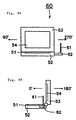
- FIG. 1A is a partial perspective front view of a portable terminal device according to an embodiment of the present invention
- Fig. 1B is a partial perspective side view thereof.
- a portable terminal device 10 has a main body 11, and a cover 13 openably and closably attached to the main body 11 by a hinge 12.
- a data entry keyboard 14 is disposed on the upper surface of the main body 11.
- the cover 13 attached to the main body 11 by the hinge 12 is retained at a position in which the cover 13 is closed to be put together with the main body 11 and at a position in which the cover 13 is stood up substantially vertically to the main body 11.
- a display 15 is disposed on the inner side of the cover 13, that is, at a position opposing the data entry keyboard 13 of the main body 11 when the cover 13 is closed.
- the display 15 is formed by a liquid crystal display or the like, and necessary information is displayed on the display 15.
- data is inputted by the data entry keyboard 14 on the main body 11.
- a chip antenna 16 is disposed at a place other than the display 15 on the inner upper part of the cover 13, e.g., as shown at the upper left, and is connected to a transmission/reception circuit disposed inside the main body 11, although this is not shown in the figure.
- Fig. 2 is a perspective view of a chip antenna used in the portable terminal device shown in Figs. 1A and 1B.
- the chip antenna 16 has a rectangular-parallelopiped base body 1, a conductor 2 formed inside the base body 1, and a feeding terminal 3 formed on a surface of the base body 1.
- the chip antenna 16 has, for example, dimensions of 9.5x2x2 (mm).
- the conductor 2 is disposed in a spiral manner in the longitudinal direction of the base body 1.
- one end of the conductor 2 is extended onto an end face of the base body 1 to be connected to the feeding terminal 3, and the other end thereof forms a free end 4 inside the base body 1.
- Fig. 3 is an exploded perspective view of the chip antenna shown in Fig. 2.
- the base body 1 is comprised of laminated rectangular dielectric-ceramic sheet layers 5a to 5c.
- the main components of the dielectric ceramic material are barium oxide, aluminum oxide, and silica.
- conductive patterns 6a to 6h are disposed by printing, evaporation, bonding together, or plating. These conductive patterns are preferably formed of copper or an alloy of copper, and they have substantially L-letter forms or substantially straight-line forms.
- Via-hole conductors 7 are formed at specified positions on the sheet layer 5b (at both ends of the conductive patterns 6e to 6g, and at an end of a conductive pattern 6h) in the thickness direction.
- FIG. 4 is a perspective view of a modified example of the chip antenna shown in Fig. 2.
- a chip antenna 16a shown in Fig. 4 has a rectangular-parallelopiped base body 1a, a conductor 2a wound in a spiral form in the longitudinal direction of the base body 1a inside the base body 1a, a ground electrode 8 opposing the conductor 2a, a feeding terminal 6a for applying voltage to the conductor 2a on a surface of the base body 1a, and a ground terminal 9 thereon, the ground terminal 9 being connected to the ground electrode 8.
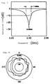
- Fig. 5 is a graph of the reflection characteristics of the chip antenna shown in Fig. 2, obtained when the chip antenna is mounted on the portable terminal device shown in Figs. 1A and 1B. In this figure, it is found that even when the chip antenna 16 is mounted on the portable terminal device 10, the chip antenna 16 provides a resonant frequency of 2.45 (GHz) and a bandwidth of 116 (MHz).
- GHz 2.45
- MHz bandwidth
- Fig. 6 is a chart illustrating the directivity of the chip antenna shown in Fig. 2 obtained when the chip antenna is mounted on the portable terminal device shown in Figs. 1A and 1B.
- a solid line indicates a case of the portable terminal device 10 of the embodiment (shown in Figs. 1A and 1B), and a broken line indicates a case of the conventional portable terminal device 60 (shown in Fig. 9).
- the range of 0° to 360° is equivalent to the range of 0° to 360° each shown in Figs. 1A, 1B and 9.
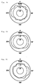
- Fig. 7A is a view of the directivity of the chip antenna shown in Fig. 2 obtained when the chip antenna is positioned at the left edge on the cover of the portable terminal device shown in Figs. 1A and 1B
- Fig. 7B is a view thereof obtained when the chip antenna is positioned substantially at the center thereon
- Fig. 7C is a view thereof obtained when the chip antenna is positioned at the right edge thereon.
- the chip antenna 16 exhibits a substantially constant gain in the range of 360°, regardless of the positions of the chip antenna 16 shown in Fig. 2 on the cover 13.
- the invention is applicable as long as the chip antenna is disposed on the cover.
- the chip antenna may be exposed on the inner side of the cover or the outer side thereof.
- antenna characteristics the case of the chip antenna shown in Fig. 2 mounted on the portable terminal device has been described. However, the same antenna characteristics can also be obtained by the chip antenna shown in Fig. 4 mounted thereon.
- the chip-antenna conductor 2, 2a may be disposed on a surface of the base body 1, 1a.
Landscapes
- Engineering & Computer Science (AREA)
- Microelectronics & Electronic Packaging (AREA)
- Support Of Aerials (AREA)
- Details Of Aerials (AREA)
Applications Claiming Priority (2)
| Application Number | Priority Date | Filing Date | Title |
|---|---|---|---|
| JP11183119A JP2001016019A (ja) | 1999-06-29 | 1999-06-29 | 携帯端末装置 |
| JP18311999 | 1999-06-29 |
Publications (2)
| Publication Number | Publication Date |
|---|---|
| EP1065582A1 true EP1065582A1 (fr) | 2001-01-03 |
| EP1065582B1 EP1065582B1 (fr) | 2004-11-10 |
Family
ID=16130130
Family Applications (1)
| Application Number | Title | Priority Date | Filing Date |
|---|---|---|---|
| EP00113267A Expired - Lifetime EP1065582B1 (fr) | 1999-06-29 | 2000-06-21 | Terminal portable avec antenne monopouce |
Country Status (4)
| Country | Link |
|---|---|
| US (1) | US6342858B1 (fr) |
| EP (1) | EP1065582B1 (fr) |
| JP (1) | JP2001016019A (fr) |
| DE (1) | DE60015657T2 (fr) |
Cited By (1)
| Publication number | Priority date | Publication date | Assignee | Title |
|---|---|---|---|---|
| WO2002084465A3 (fr) * | 2001-04-12 | 2003-11-06 | Siemens Ag | Unite de calcul mobile |
Families Citing this family (12)
| Publication number | Priority date | Publication date | Assignee | Title |
|---|---|---|---|---|
| DE60120894T2 (de) * | 2000-12-26 | 2007-01-11 | The Furukawa Electric Co., Ltd. | Herstellungsverfahren einer Antenne |
| US6538606B2 (en) | 2001-01-26 | 2003-03-25 | Dell Products L.P. | Antenna module interface extension |
| US6922575B1 (en) | 2001-03-01 | 2005-07-26 | Symbol Technologies, Inc. | Communications system and method utilizing integrated chip antenna |
| KR100400563B1 (ko) * | 2001-04-11 | 2003-10-08 | 엘지전자 주식회사 | 무선통신용 안테나 및 그 안테나를 갖는 이동 컴퓨터 |
| US7605177B2 (en) * | 2001-05-24 | 2009-10-20 | Neuren Pharmaceuticals Limited | Effects of glycyl-2 methyl prolyl glutamate on neurodegeneration |
| US6567049B1 (en) * | 2002-01-22 | 2003-05-20 | King Sound Enterprise Co., Ltd. | Method for manufacturing chip antenna by utilizing genetic algorithm |
| US6677906B2 (en) | 2002-04-17 | 2004-01-13 | Dell Products L.P. | Glass antenna for laptop computers |
| US6927760B2 (en) * | 2002-10-03 | 2005-08-09 | Darfon Electronics Corp. | Wireless keyboard with improving radiation transmission |
| FI116333B (fi) * | 2003-09-11 | 2005-10-31 | Lk Products Oy | Menetelmä säteilijän asentamiseksi radiolaitteeseen ja radiolaite |
| JP4271647B2 (ja) * | 2004-11-01 | 2009-06-03 | 三菱電機株式会社 | 表示装置 |
| JP2005102286A (ja) * | 2004-11-08 | 2005-04-14 | Toshiba Corp | 電子機器 |
| CN103840256B (zh) * | 2012-11-27 | 2016-10-05 | 联想(北京)有限公司 | 便携式终端 |
Citations (4)
| Publication number | Priority date | Publication date | Assignee | Title |
|---|---|---|---|---|
| EP0762536A2 (fr) * | 1995-09-05 | 1997-03-12 | Murata Manufacturing Co., Ltd. | Antenne pastille |
| EP0790662A1 (fr) * | 1996-02-14 | 1997-08-20 | Murata Manufacturing Co., Ltd. | Antenne pour montage en surface et appareil de communication utilisant celle-ci |
| WO1997044946A1 (fr) * | 1996-05-04 | 1997-11-27 | Hugh Symons Group Plc | Terminal de donnees portable |
| EP0825669A2 (fr) * | 1996-08-23 | 1998-02-25 | Murata Manufacturing Co., Ltd. | Dispositif mobile de communication |
Family Cites Families (5)
| Publication number | Priority date | Publication date | Assignee | Title |
|---|---|---|---|---|
| US5966098A (en) * | 1996-09-18 | 1999-10-12 | Research In Motion Limited | Antenna system for an RF data communications device |
| JP2996191B2 (ja) * | 1996-12-25 | 1999-12-27 | 株式会社村田製作所 | チップアンテナ |
| US5995052A (en) * | 1998-05-15 | 1999-11-30 | Ericsson Inc. | Flip open antenna for a communication device |
| US5943021A (en) * | 1998-08-03 | 1999-08-24 | Ericsson Inc. | Swivel antenna with parasitic tuning |
| US6181284B1 (en) * | 1999-05-28 | 2001-01-30 | 3 Com Corporation | Antenna for portable computers |
-
1999
- 1999-06-29 JP JP11183119A patent/JP2001016019A/ja active Pending
-
2000
- 2000-05-22 US US09/575,424 patent/US6342858B1/en not_active Expired - Fee Related
- 2000-06-21 EP EP00113267A patent/EP1065582B1/fr not_active Expired - Lifetime
- 2000-06-21 DE DE60015657T patent/DE60015657T2/de not_active Expired - Fee Related
Patent Citations (4)
| Publication number | Priority date | Publication date | Assignee | Title |
|---|---|---|---|---|
| EP0762536A2 (fr) * | 1995-09-05 | 1997-03-12 | Murata Manufacturing Co., Ltd. | Antenne pastille |
| EP0790662A1 (fr) * | 1996-02-14 | 1997-08-20 | Murata Manufacturing Co., Ltd. | Antenne pour montage en surface et appareil de communication utilisant celle-ci |
| WO1997044946A1 (fr) * | 1996-05-04 | 1997-11-27 | Hugh Symons Group Plc | Terminal de donnees portable |
| EP0825669A2 (fr) * | 1996-08-23 | 1998-02-25 | Murata Manufacturing Co., Ltd. | Dispositif mobile de communication |
Non-Patent Citations (1)
| Title |
|---|
| ANON.: "Antenna Array and Housing for Notebook Computers", IBM TECHNICAL DISCLOSURE BULLETIN, vol. 39, no. 1, January 1996 (1996-01-01), NEW YORK US, pages 313 - 314, XP000556415 * |
Cited By (1)
| Publication number | Priority date | Publication date | Assignee | Title |
|---|---|---|---|---|
| WO2002084465A3 (fr) * | 2001-04-12 | 2003-11-06 | Siemens Ag | Unite de calcul mobile |
Also Published As
| Publication number | Publication date |
|---|---|
| DE60015657T2 (de) | 2005-10-27 |
| EP1065582B1 (fr) | 2004-11-10 |
| DE60015657D1 (de) | 2004-12-16 |
| JP2001016019A (ja) | 2001-01-19 |
| US6342858B1 (en) | 2002-01-29 |
Similar Documents
| Publication | Publication Date | Title |
|---|---|---|
| US6184833B1 (en) | Dual strip antenna | |
| US5680144A (en) | Wideband, stacked double C-patch antenna having gap-coupled parasitic elements | |
| US6728559B2 (en) | Radio communication device and electronic apparatus having the same | |
| US5945954A (en) | Antenna assembly for telecommunication devices | |
| US6373436B1 (en) | Dual strip antenna with periodic mesh pattern | |
| US5627550A (en) | Wideband double C-patch antenna including gap-coupled parasitic elements | |
| EP1072064B1 (fr) | Antenne monoplan a deux bandes | |
| US6686886B2 (en) | Integrated antenna for laptop applications | |
| US5657028A (en) | Small double C-patch antenna contained in a standard PC card | |
| US6642892B2 (en) | Antenna and electronic device containing the same | |
| US6268831B1 (en) | Inverted-f antennas with multiple planar radiating elements and wireless communicators incorporating same | |
| US7079077B2 (en) | Methods and apparatus for implementation of an antenna for a wireless communication device | |
| KR100605421B1 (ko) | 평판 다중 안테나 및 휴대용 단말기 | |
| EP1065582B1 (fr) | Terminal portable avec antenne monopouce | |
| US7205944B2 (en) | Methods and apparatus for implementation of an antenna for a wireless communication device | |
| WO2003094373A1 (fr) | Ensemble antenne integre | |
| US7233289B2 (en) | Multiple-frequency antenna structure | |
| JPH11340726A (ja) | アンテナ装置 | |
| JP2003158410A (ja) | アンテナモジュール | |
| JP3769196B2 (ja) | プレートアンテナ及びそのアンテナを備える通信放送端末 | |
| JP4067041B2 (ja) | プレートアンテナおよびそのアンテナを備える通信端末 | |
| JPH09199939A (ja) | アンテナシステム | |
| EP0825669A2 (fr) | Dispositif mobile de communication | |
| JP2005117678A (ja) | 携帯端末装置 | |
| JP2004228940A (ja) | 無線機用逆fアンテナ |
Legal Events
| Date | Code | Title | Description |
|---|---|---|---|
| PUAI | Public reference made under article 153(3) epc to a published international application that has entered the european phase |
Free format text: ORIGINAL CODE: 0009012 |
|
| 17P | Request for examination filed |
Effective date: 20000621 |
|
| AK | Designated contracting states |
Kind code of ref document: A1 Designated state(s): DE FI FR SE |
|
| AX | Request for extension of the european patent |
Free format text: AL;LT;LV;MK;RO;SI |
|
| AKX | Designation fees paid |
Free format text: DE FI FR SE |
|
| GRAP | Despatch of communication of intention to grant a patent |
Free format text: ORIGINAL CODE: EPIDOSNIGR1 |
|
| GRAS | Grant fee paid |
Free format text: ORIGINAL CODE: EPIDOSNIGR3 |
|
| GRAA | (expected) grant |
Free format text: ORIGINAL CODE: 0009210 |
|
| AK | Designated contracting states |
Kind code of ref document: B1 Designated state(s): DE FI FR SE |
|
| REF | Corresponds to: |
Ref document number: 60015657 Country of ref document: DE Date of ref document: 20041216 Kind code of ref document: P |
|
| REG | Reference to a national code |
Ref country code: SE Ref legal event code: TRGR |
|
| PGFP | Annual fee paid to national office [announced via postgrant information from national office to epo] |
Ref country code: SE Payment date: 20050617 Year of fee payment: 6 |
|
| PGFP | Annual fee paid to national office [announced via postgrant information from national office to epo] |
Ref country code: FI Payment date: 20050620 Year of fee payment: 6 |
|
| PLBE | No opposition filed within time limit |
Free format text: ORIGINAL CODE: 0009261 |
|
| STAA | Information on the status of an ep patent application or granted ep patent |
Free format text: STATUS: NO OPPOSITION FILED WITHIN TIME LIMIT |
|
| 26N | No opposition filed |
Effective date: 20050811 |
|
| ET | Fr: translation filed | ||
| PG25 | Lapsed in a contracting state [announced via postgrant information from national office to epo] |
Ref country code: FI Free format text: LAPSE BECAUSE OF NON-PAYMENT OF DUE FEES Effective date: 20060621 |
|
| PG25 | Lapsed in a contracting state [announced via postgrant information from national office to epo] |
Ref country code: SE Free format text: LAPSE BECAUSE OF NON-PAYMENT OF DUE FEES Effective date: 20060622 |
|
| EUG | Se: european patent has lapsed | ||
| PGFP | Annual fee paid to national office [announced via postgrant information from national office to epo] |
Ref country code: DE Payment date: 20080626 Year of fee payment: 9 |
|
| PGFP | Annual fee paid to national office [announced via postgrant information from national office to epo] |
Ref country code: FR Payment date: 20080617 Year of fee payment: 9 |
|
| REG | Reference to a national code |
Ref country code: FR Ref legal event code: ST Effective date: 20100226 |
|
| PG25 | Lapsed in a contracting state [announced via postgrant information from national office to epo] |
Ref country code: FR Free format text: LAPSE BECAUSE OF NON-PAYMENT OF DUE FEES Effective date: 20090630 |
|
| PG25 | Lapsed in a contracting state [announced via postgrant information from national office to epo] |
Ref country code: DE Free format text: LAPSE BECAUSE OF NON-PAYMENT OF DUE FEES Effective date: 20100101 |