EP1065624A2 - Chipmodul zum Einbau in einen Chipkartenträger - Google Patents
Chipmodul zum Einbau in einen Chipkartenträger Download PDFInfo
- Publication number
- EP1065624A2 EP1065624A2 EP00113089A EP00113089A EP1065624A2 EP 1065624 A2 EP1065624 A2 EP 1065624A2 EP 00113089 A EP00113089 A EP 00113089A EP 00113089 A EP00113089 A EP 00113089A EP 1065624 A2 EP1065624 A2 EP 1065624A2
- Authority
- EP
- European Patent Office
- Prior art keywords
- chip
- contact
- component
- module
- contact surface
- Prior art date
- Legal status (The legal status is an assumption and is not a legal conclusion. Google has not performed a legal analysis and makes no representation as to the accuracy of the status listed.)
- Granted
Links
Images
Classifications
-
- G—PHYSICS
- G06—COMPUTING OR CALCULATING; COUNTING
- G06K—GRAPHICAL DATA READING; PRESENTATION OF DATA; RECORD CARRIERS; HANDLING RECORD CARRIERS
- G06K19/00—Record carriers for use with machines and with at least a part designed to carry digital markings
- G06K19/06—Record carriers for use with machines and with at least a part designed to carry digital markings characterised by the kind of the digital marking, e.g. shape, nature, code
- G06K19/067—Record carriers with conductive marks, printed circuits or semiconductor circuit elements, e.g. credit or identity cards also with resonating or responding marks without active components
- G06K19/07—Record carriers with conductive marks, printed circuits or semiconductor circuit elements, e.g. credit or identity cards also with resonating or responding marks without active components with integrated circuit chips
- G06K19/077—Constructional details, e.g. mounting of circuits in the carrier
- G06K19/07749—Constructional details, e.g. mounting of circuits in the carrier the record carrier being capable of non-contact communication, e.g. constructional details of the antenna of a non-contact smart card
- G06K19/07766—Constructional details, e.g. mounting of circuits in the carrier the record carrier being capable of non-contact communication, e.g. constructional details of the antenna of a non-contact smart card comprising at least a second communication arrangement in addition to a first non-contact communication arrangement
- G06K19/07769—Constructional details, e.g. mounting of circuits in the carrier the record carrier being capable of non-contact communication, e.g. constructional details of the antenna of a non-contact smart card comprising at least a second communication arrangement in addition to a first non-contact communication arrangement the further communication means being a galvanic interface, e.g. hybrid or mixed smart cards having a contact and a non-contact interface
-
- G—PHYSICS
- G06—COMPUTING OR CALCULATING; COUNTING
- G06K—GRAPHICAL DATA READING; PRESENTATION OF DATA; RECORD CARRIERS; HANDLING RECORD CARRIERS
- G06K19/00—Record carriers for use with machines and with at least a part designed to carry digital markings
- G06K19/06—Record carriers for use with machines and with at least a part designed to carry digital markings characterised by the kind of the digital marking, e.g. shape, nature, code
- G06K19/067—Record carriers with conductive marks, printed circuits or semiconductor circuit elements, e.g. credit or identity cards also with resonating or responding marks without active components
- G06K19/07—Record carriers with conductive marks, printed circuits or semiconductor circuit elements, e.g. credit or identity cards also with resonating or responding marks without active components with integrated circuit chips
- G06K19/077—Constructional details, e.g. mounting of circuits in the carrier
- G06K19/07745—Mounting details of integrated circuit chips
-
- G—PHYSICS
- G06—COMPUTING OR CALCULATING; COUNTING
- G06K—GRAPHICAL DATA READING; PRESENTATION OF DATA; RECORD CARRIERS; HANDLING RECORD CARRIERS
- G06K19/00—Record carriers for use with machines and with at least a part designed to carry digital markings
- G06K19/06—Record carriers for use with machines and with at least a part designed to carry digital markings characterised by the kind of the digital marking, e.g. shape, nature, code
- G06K19/067—Record carriers with conductive marks, printed circuits or semiconductor circuit elements, e.g. credit or identity cards also with resonating or responding marks without active components
- G06K19/07—Record carriers with conductive marks, printed circuits or semiconductor circuit elements, e.g. credit or identity cards also with resonating or responding marks without active components with integrated circuit chips
- G06K19/077—Constructional details, e.g. mounting of circuits in the carrier
- G06K19/07749—Constructional details, e.g. mounting of circuits in the carrier the record carrier being capable of non-contact communication, e.g. constructional details of the antenna of a non-contact smart card
-
- G—PHYSICS
- G06—COMPUTING OR CALCULATING; COUNTING
- G06K—GRAPHICAL DATA READING; PRESENTATION OF DATA; RECORD CARRIERS; HANDLING RECORD CARRIERS
- G06K19/00—Record carriers for use with machines and with at least a part designed to carry digital markings
- G06K19/06—Record carriers for use with machines and with at least a part designed to carry digital markings characterised by the kind of the digital marking, e.g. shape, nature, code
- G06K19/067—Record carriers with conductive marks, printed circuits or semiconductor circuit elements, e.g. credit or identity cards also with resonating or responding marks without active components
- G06K19/07—Record carriers with conductive marks, printed circuits or semiconductor circuit elements, e.g. credit or identity cards also with resonating or responding marks without active components with integrated circuit chips
- G06K19/077—Constructional details, e.g. mounting of circuits in the carrier
- G06K19/07749—Constructional details, e.g. mounting of circuits in the carrier the record carrier being capable of non-contact communication, e.g. constructional details of the antenna of a non-contact smart card
- G06K19/0775—Constructional details, e.g. mounting of circuits in the carrier the record carrier being capable of non-contact communication, e.g. constructional details of the antenna of a non-contact smart card arrangements for connecting the integrated circuit to the antenna
- G06K19/07752—Constructional details, e.g. mounting of circuits in the carrier the record carrier being capable of non-contact communication, e.g. constructional details of the antenna of a non-contact smart card arrangements for connecting the integrated circuit to the antenna using an interposer
-
- H—ELECTRICITY
- H05—ELECTRIC TECHNIQUES NOT OTHERWISE PROVIDED FOR
- H05K—PRINTED CIRCUITS; CASINGS OR CONSTRUCTIONAL DETAILS OF ELECTRIC APPARATUS; MANUFACTURE OF ASSEMBLAGES OF ELECTRICAL COMPONENTS
- H05K1/00—Printed circuits
- H05K1/18—Printed circuits structurally associated with non-printed electric components
- H05K1/182—Printed circuits structurally associated with non-printed electric components associated with components mounted in printed circuit boards [PCB], e.g. insert-mounted components [IMC]
- H05K1/183—Printed circuits structurally associated with non-printed electric components associated with components mounted in printed circuit boards [PCB], e.g. insert-mounted components [IMC] associated with components mounted in and supported by recessed areas of the PCBs
-
- H—ELECTRICITY
- H10—SEMICONDUCTOR DEVICES; ELECTRIC SOLID-STATE DEVICES NOT OTHERWISE PROVIDED FOR
- H10W—GENERIC PACKAGES, INTERCONNECTIONS, CONNECTORS OR OTHER CONSTRUCTIONAL DETAILS OF DEVICES COVERED BY CLASS H10
- H10W72/00—Interconnections or connectors in packages
- H10W72/50—Bond wires
- H10W72/551—Materials of bond wires
- H10W72/552—Materials of bond wires comprising metals or metalloids, e.g. silver
- H10W72/5522—Materials of bond wires comprising metals or metalloids, e.g. silver comprising gold [Au]
-
- H—ELECTRICITY
- H10—SEMICONDUCTOR DEVICES; ELECTRIC SOLID-STATE DEVICES NOT OTHERWISE PROVIDED FOR
- H10W—GENERIC PACKAGES, INTERCONNECTIONS, CONNECTORS OR OTHER CONSTRUCTIONAL DETAILS OF DEVICES COVERED BY CLASS H10
- H10W90/00—Package configurations
- H10W90/701—Package configurations characterised by the relative positions of pads or connectors relative to package parts
- H10W90/751—Package configurations characterised by the relative positions of pads or connectors relative to package parts of bond wires
- H10W90/754—Package configurations characterised by the relative positions of pads or connectors relative to package parts of bond wires between a chip and a stacked insulating package substrate, interposer or RDL
Definitions
- the present invention relates to a chip module with a module carrier with at least one electrical contact surface on one side of the module carrier, at least one electrical component on the opposite Side of the module carrier and openings for contacting the Contact area and the component.
- the invention further relates to a chip card with at least one such chip module, the electrical contact area of the chip module connected to a component in the chip card body are.
- the invention also relates to methods of manufacture of the chip module and the chip card.
- the chip card has in its chip card body a corresponding component for contactless data transmission on, for example an antenna or an antenna coil.
- the appropriate interface that is, either with contact areas or be equipped with an antenna.
- the external contact surfaces are usually on the outside of a so-called chip module, which is on the opposite An electrical component, that is to say the actual chip, bears on the inside.
- the chip is contacted with the contact areas through the module carrier.
- the contacting is usually carried out by means of the bonding process. Fine wires become from the contacts of the chip through openings in the module carrier to the contact areas During the production of a card which only allows data exchange via the contact areas, this finished chip module is glued, for example, into a plastic chip card body with a corresponding recess.
- This type of contacting is also called flip-chip technology (see Lexicon Electronics and Microelectronics ", 2nd edition, VDI-Verlag 1993, p.330).
- So-called Ball Bumps is used.
- a wire is bonded to one of the components and melted or torn off, for example, by increasing the bonding current.
- This creates an electrically conductive elevation which, when the components are placed one on the other, is pressed into a contact point of the opposite component and establishes the electrical connection.
- Similar techniques are also described in WO 96/24944 and EP 0 094 716. A great advantage of these techniques is that no additional joining techniques, such as conductive gluing, soldering, welding or the like, are required.
- the technology itself is on use limited to flip chips, where the one electrical component directly on the other component is put on. It is therefore necessary that the chip module or the module carrier also on the side on which the chip is located, Has contact surfaces, which then when the chip module is inserted in the chip card body via ball bumps or the like with the interface component get connected.
- a so-called double-sided module carrier tape as the starting material used, which has contact surfaces on both sides.
- the task is to create an inexpensive alternative to this known one To create state of the art.
- the chip module or chip card according to the invention are can be produced by processes according to the subordinate process claims.
- the basic idea of the invention is that on the component Side of the module carrier of the chip module at least one contact bridge is arranged, which at both ends through openings connected to the outside contact surface in the module carrier is. Then over the contact bridge when inserting the chip module in the chip card body a contact between the contact areas on the Outside of the chip module and the contacts of the interface component getting produced.
- This connection solution is therefore not double-sided Module carrier tape required, but it can be a cheaper one Module carrier tape can be used as it is for the manufacture is used by simple chip cards that are only used for data exchange are provided over contact areas. Because the junctions of the contact bridges with the contact surfaces themselves within the openings of the module carrier, these connection points are also through the Module carrier protected so that they are in the implantation of the chip module The chip card body cannot be loaded or torn off.
- the contact bridges can be made of any electrically conductive Material.
- it is preferably bond wire whereby under bond wire in this sense a wire, for example a fine gold wire, is to be understood to be used for bonding with conventional ones Process and facilities is suitable.
- the adhesive layer is preferably an adhesive film, for example a thermal adhesive or the like that laminates onto the module carrier becomes.
- the recesses can, for example, before being applied to the Module carriers are punched into the adhesive film.
- Such a chip module has the advantage that the contact bridges gentle when implanting into the chip card body through the adhesive layer be padded.
- the connection point between the contact bridges and the contacts of the interface component is through the adhesive layer well protected against dynamic stress. Will continue the pressure load on the contacts when implanting through the adhesive "frozen”. This leads to a stable and low contact resistance.
- the adhesive layer also advantageously has a recess for the chip on.
- the chip is then only after the application of the adhesive layer potted in a known manner with a potting compound, the Edge of the recess serves as a potting edge and so a simple way clean sealing of the sealing compound is achieved.
- connection bridges You can also use the contact bridges to protect the connection points the contact area these are cast locally with a potting compound by for example the openings in the module carrier with sealing compound be replenished. This increases the stability of the connection points elevated.
- the chip modules are then, as usual, into a correspondingly shaped one Recess used in a chip card body, the contact bridges on the chip module, the contacts of the component in the Charge the chip card body.
- Adhesive layer is used to place the chip module in the chip card body glue in.
- the invention is mainly used for dual interface cards, wherein the component in the chip card body is an interface component for contactless data transmission is. Of course it is not open limited this application. In the component in the chip card body it can also be any other components, for example for contacts that lead to another chip or chip module.
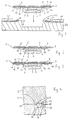
- the chip module 1 consists of a module carrier 2, on which one side, the later outside, the electrical contact surfaces 3 are located. On the contact surfaces 3 opposite inside of the chip module is the electrical one Component 4, that is the chip 4, arranged.
- the module carriers 2 are usually made from a ready-made Module carrier tape manufactured. The are on this module carrier tape Chips 4 placed and then bonded to the contact areas 3.
- the production the contact bridges 10 is with the same devices and the same Methods such as bonding between the chip 4 and the contact areas 3 possible.
- the production of a chip module 1 according to the invention requires consequently only a further process step in which the contact bridges 10 can be bonded.
- the manufacture of the openings 11 for the contact bridges 10 can be manufactured in one operation with the Opening 5 for the bond wires 6 between the chip 4 and the contact areas 3 done. The additional effort in the manufacture of such chip modules 1 compared to conventional chip modules is therefore low.
- the finished chip modules 1 are then in corresponding recesses 23 used in the chip card body 20.
- the recess 23 consists of a first section 24, which is connected to the external dimensions of the module carrier 2 is adapted so that the module carrier 2 is flush with the surface of the chip card body 20 can be inserted into the recess 23.
- this first recess section 23 is a further section 25 in the form of a pot-like recess 25, in which the potting compound 7 encased chip 4 fits into it.
- the contacts 22 in the recess 24 or the contact bridges 10 am Chip module 1 are aligned such that when the chip module 1 is inserted the recess 23 of the chip card body 20 the contact bridges 10 the associated Contact contacts 22. In this way, between the Contact surfaces 3 and the contacts 22 of the antenna coil 21 a contact manufactured.
- the antenna coil 21 is thus also included via the bonding wires 6 connected to the chip 4.
- each 3 there is a contact surface for each 3 at least two contact bridges 10 connected in parallel to each other.
- the two ends 12, 13 are in each case a contact bridge 10 with different bonding methods with the Contact surface 3 connected, also taking care that the in each case adjacent ends 12, 13 of the parallel Contact bridges 10 also with the different bonding methods are connected to the contact surface 3.
- two parallel contact bridges 10 connected to the contact surface 3 that each of the ends 12 lying over one another with a bonding process, for example a "ball” process, and the other two ends 13 each with a different bonding method, for example one "Wedge” process to be attached.
- This redundant arrangement the contact bridges 10 ensures the highest possible contact reliability.
- FIG. 2 shows an alternative embodiment of the invention Chip module 1.
- Chip module 1 in addition to the cutouts 5 for the bond wires 6 only one more between the chip 4 and the contact surfaces 3 Opening 11 introduced into the module carrier 2 per contact bridge 10.
- the contact bridges 10 were then between the openings 5 and the further outer openings 11 are drawn. So it becomes a Bond position saved.
- the respective Contact bridge 10 are pulled.
- the exemplary embodiment according to FIG. 3 offers further additional advantages.
- This adhesive film 15 is in Area of the openings 11 of the module carrier 2 and in the area of Chips 4 punched out.
- the edge 17 of the recess 16 of the adhesive film 15 around the chip 4 can be used as a potting edge, so that there is automatically a limit for the potting compound 7.
- Chip module 1 glued into the chip card body 20.
- the adhesive film 15 For example, it can be a thermal adhesive that is under the cures at the appropriate temperature.
- the contact bridges 10 are during implantation gently padded.
- the contact bridges are in the finished chip card or the contacts of the antenna coil 21 through the adhesive film 15 against dynamic Load secured.
- the pressure load on the contacts 22 are fixed during implantation by the adhesive, thereby creating a stable and low contact resistance is guaranteed.
- connection points the contact bridges 10 with the contact surfaces 3 locally with a Pouring resin, that is, the openings 11 in the module carrier 2 filled with a potting compound. This will ensure the security of the Contacting when installing the chip module 1 in the chip card body 20 elevated.
Landscapes
- Engineering & Computer Science (AREA)
- Microelectronics & Electronic Packaging (AREA)
- Computer Hardware Design (AREA)
- Physics & Mathematics (AREA)
- General Physics & Mathematics (AREA)
- Theoretical Computer Science (AREA)
- Credit Cards Or The Like (AREA)
- Encapsulation Of And Coatings For Semiconductor Or Solid State Devices (AREA)
Abstract

Description

Claims (22)
- Chipmodul (1) mit einem Modulträger (2) mit mindestens einer elektrischen Kontaktfläche (3) auf einer Seite des Modulträgers (2) und mindestens einem elektrischen Bauteil (4) auf der gegenüberliegenden Seite des Modulträgers (2) und mit Durchbrechungen (5) für die Kontaktierung (6) der Kontaktfläche (3) und des Bauteils (4), dadurch gekennzeichnet, daß auf der das Bauteil (4) aufweisenden Seite des Modulträgers (2) mindestens eine Kontaktbrücke (10) angeordnet ist, welche an ihren beiden Enden (12, 13) durch Durchbrechungen (11) im Modulträger (2) hindurch mit der Kontaktfläche (3) verbunden ist.
- Chipmodul nach Anspruch 1, dadurch gekennzeichnet, daß die Kontaktbrücke (10) aus Bonddraht besteht.
- Chipmodul nach Anspruch 1 oder 2, dadurch gekennzeichnet, daß eines der Enden (12, 13) der Kontaktbrücke (10) durch eine Durchbrechung (5) für die Kontaktierung (6) der Kontaktfläche (3) mit dem Bauteil (4) durchgeführt ist.
- Chipmodul nach einem der Ansprüche 1 bis 3, gekennzeichnet durch mindestens zwei parallel zueinander mit der Kontaktfläche (3) verbundene Kontaktbrücken (10).
- Chipmodul nach einem der Ansprüche 1 bis 4, dadurch gekennzeichnet, daß die beiden Enden (12,13) der Kontaktbrücke(n) (10) mittels unterschiedlicher Bondingrnethoden mit der Kontaktfläche (3) verbunden sind.
- Chipmodul nach Anspruch 4 oder 5, dadurch gekennzeichnet, daß die jeweils zueinander benachbart angeordneten Enden (12, 13) paralleler Kontaktbrücken (10) mittels unterschiedlicher Bondingmethoden mit der Kontaktfläche (3) verbunden sind.
- Chipmodul nach einem der Ansprüche 1 bis 6, dadurch gekennzeichnet, daß der Modulträger (2) eine sich zwischen dem Modulträger (2) und der/den Kontaktbrücke(n) (10) auf der bauteilseitigen Oberfläche erstrekkende Kleberschicht (15) aufweist, welche an den Durchbrechungen (11) des Modulträgers (2) Aussparungen (18) für den Durchtritt der Kontaktbrücke(n) (10)aufweist.
- Chipmodul nach einem der Ansprüche 1 bis 7, dadurch gekennzeichnet, daß die Verbindungsstellen der Kontaktbrücke(n) (10) mit der Kontaktfläche (3) von einer Vergußmasse umgeben sind.
- Chipkarte mit mindestens einem Chipmodul (1) mit mindestens einer elektrischen Kontaktfläche (3), die mit einem Bauelement (21) im Chipkartenkörper (20) verbunden ist, gekennzeichnet durch ein Chipmodul (1) nach einem der Ansprüche 1 bis 8, wobei mindestens eine Kontaktbrücke (10) die elektrische Kontaktfläche (3) mit dem Bauelement (21) im Chipkartenkörper (20) verbindet.
- Chipkarte nach Anspruch 9, dadurch gekennzeichnet, daß die Chipkarte eine Dual-Interface-Karte und das Bauelement (21) im Chipkartenkörper (20) ein Interfacebauelement (21) zur kontaktlosen Datenübertragung ist.
- Verfahren zur Herstellung eines Chipmoduls (1), bei dem ein Modulträger (2) auf einer Seite mit mindestens einer elektrischen Kontaktfläche (3), auf der gegenüberliegenden Seite mit mindestens einem elektrischen Bauteil (4) und mit Durchbrechungen (5) für die Kontaktierung (6) der Kontaktfläche (3) und des Bauteils (4) versehen wird, dadurch gekennzeichnet, daß auf der das Bauteil (4) aufweisenden Seite des Modulträgers (2) mindestens eine Kontaktbrücke (10) angeordnet wird, welche an ihren beiden Enden (12, 13) durch im Modulträger (2) eingebrachte Durchbrechungen (11) hindurch mit der Kontaktfläche (3) verbunden wird.
- Verfahren nach Anspruch 11, dadurch gekennzeichnet, daß die Kontaktbrücke (10) aus Draht gebondet wird.
- Verfahren nach Anspruch 11 oder 12, dadurch gekennzeichnet, daß eines der Enden (12, 13) der Kontaktbrücke (10) durch eine Durchbrechung (5) für die Kontaktierung (6) der Kontaktfläche (3) mit dem Bauteil (4) durchgeführt wird.
- Verfahren nach einem der Ansprüche 11 bis 13, dadurch gekennzeichnet, daß mindestens zwei Kontaktbrücken (10) parallel zueinander mit der jeweiligen Kontaktfläche (3) verbunden werden.
- Verfahren nach einem der Ansprüche 11 bis 14, dadurch gekennzeichnet, daß die beiden Enden (12, 13) der Kontaktbrücke(n) (10) mittels unterschiedlicher Bondingmethoden mit der Kontaktfläche (3) verbunden werden.
- Verfahren nach Anspruch 14 oder 15, dadurch gekennzeichnet, daß die jeweils zueinander benachbart angeordneten Enden (12, 13) paralleler Kontaktbrücken (10) mittels unterschiedlicher Bondinginethoden mit der Kontaktfläche (3) verbunden werden.
- Verfahren nach einem der Ansprüche 11 bis 16, dadurch gekennzeichnet, daß auf den Modulträger (2) auf der bauteilseitigen Oberfläche vor dem Herstellen der Kontaktbrücke(n) (10) eine Kleberschicht (15) aufgebracht wird, welche an den Durchbrechungen (11) des Modulträgers (2) Aussparungen (18) für den Durchtritt der Kontaktbrücke(n) (10) aufweist.
- Verfahren nach Anspruch 17, dadurch gekennzeichnet, daß die Kleberschicht (15) eine Aussparung (16) für das Bauteil (4) aufweist und das Bauteil (4) nach dem Aufbringen der Kleberschicht (15) mit einer Vergußmasse (7) vergossen wird.
- Verfahren nach einem der Ansprüche 11 bis 18, dadurch gekennzeichnet, daß die Verbindungsstellen der Kontaktbrücke(n) (10) mit der Kontaktfläche (3) mit einer Vergußmasse vergossen werden.
- Verfahren zur Herstellung einer Chipkarte,
bei dem in einen Chipkartenkörper (20) ein Chipmodul (1) eingebracht wird, und dabei mindestens eine Kontaktfläche (3) des Chipmoduls (1) mit mindestens einem Bauelement (21) in dem Chipkartenkörper (20) elektrisch verbunden wird, dadurch gekennzeichnet, daß in den Chipkartenkörper (20) ein nach einem Verfahren gemäß einem der Ansprüche 11 bis 19 hergestelltes Chipmodul (1) eingebracht wird, und dabei die Verbindung zwischen der Kontaktfläche (3) des Chipmoduls (1) mit dem Bauelement (21) im Chipkartenkörper (20) mittels der Kontaktbrücke(n) (10) des Chipmoduls (1) erfolgt. - Verfahren nach Anspruch 20, dadurch gekennzeichnet, daß das Chipmodul (1) mit einer Kleberschicht (15) in eine Aussparung (23) des Chipkartenkörpers (20) eingeklebt wird.
- Verfahren nach Anspruch 20 oder 21, dadurch gekennzeichnet, daß die Chipkarte eine Dual-Interface-Karte ist und in den Chipkartenkörper (20) ein Interfacebauelement (21) zur kontaktlosen Datenübertragung eingebracht wird.
Applications Claiming Priority (2)
| Application Number | Priority Date | Filing Date | Title |
|---|---|---|---|
| DE19929610 | 1999-06-28 | ||
| DE19929610A DE19929610C1 (de) | 1999-06-28 | 1999-06-28 | Chipmodul, Chipkarte und Verfahren zu deren Herstellung |
Publications (3)
| Publication Number | Publication Date |
|---|---|
| EP1065624A2 true EP1065624A2 (de) | 2001-01-03 |
| EP1065624A3 EP1065624A3 (de) | 2002-01-02 |
| EP1065624B1 EP1065624B1 (de) | 2004-03-03 |
Family
ID=7912842
Family Applications (1)
| Application Number | Title | Priority Date | Filing Date |
|---|---|---|---|
| EP00113089A Expired - Lifetime EP1065624B1 (de) | 1999-06-28 | 2000-06-27 | Chipmodul zum Einbau in einen Chipkartenträger |
Country Status (4)
| Country | Link |
|---|---|
| EP (1) | EP1065624B1 (de) |
| AT (1) | ATE261153T1 (de) |
| DE (2) | DE19929610C1 (de) |
| ES (1) | ES2216768T3 (de) |
Cited By (1)
| Publication number | Priority date | Publication date | Assignee | Title |
|---|---|---|---|---|
| EP4296894A4 (de) * | 2021-02-17 | 2024-04-03 | Fujitsu Frontech Limited | Rfid-etikett |
Families Citing this family (16)
| Publication number | Priority date | Publication date | Assignee | Title |
|---|---|---|---|---|
| US6468638B2 (en) | 1999-03-16 | 2002-10-22 | Alien Technology Corporation | Web process interconnect in electronic assemblies |
| US6606247B2 (en) | 2001-05-31 | 2003-08-12 | Alien Technology Corporation | Multi-feature-size electronic structures |
| DE10146870B4 (de) * | 2001-09-24 | 2013-03-28 | Morpho Cards Gmbh | Chipkarte und Verfahren zur Herstellung einer elektrischen Verbindung zwischen Bauelementen einer derartigen Chipkarte |
| US7214569B2 (en) | 2002-01-23 | 2007-05-08 | Alien Technology Corporation | Apparatus incorporating small-feature-size and large-feature-size components and method for making same |
| DE10234751B4 (de) * | 2002-07-30 | 2007-06-28 | Sagem Orga Gmbh | Verfahren zur Herstellung einer spritzgegossenen Chipkarte und nach dem Verfahren hergestellte Chipkarte |
| US7253735B2 (en) | 2003-03-24 | 2007-08-07 | Alien Technology Corporation | RFID tags and processes for producing RFID tags |
| DE10327126B4 (de) * | 2003-06-13 | 2005-07-14 | W.C. Heraeus Gmbh | Verfahren zur Herstellung von Chipmodulen |
| US7615479B1 (en) | 2004-11-08 | 2009-11-10 | Alien Technology Corporation | Assembly comprising functional block deposited therein |
| US7551141B1 (en) | 2004-11-08 | 2009-06-23 | Alien Technology Corporation | RFID strap capacitively coupled and method of making same |
| US7385284B2 (en) | 2004-11-22 | 2008-06-10 | Alien Technology Corporation | Transponder incorporated into an electronic device |
| US7688206B2 (en) | 2004-11-22 | 2010-03-30 | Alien Technology Corporation | Radio frequency identification (RFID) tag for an item having a conductive layer included or attached |
| DE102005002732A1 (de) * | 2005-01-20 | 2006-08-03 | Giesecke & Devrient Gmbh | Tragbarer Datenträger |
| US7542301B1 (en) | 2005-06-22 | 2009-06-02 | Alien Technology Corporation | Creating recessed regions in a substrate and assemblies having such recessed regions |
| DE102006019925B4 (de) * | 2006-04-28 | 2010-09-16 | Infineon Technologies Ag | Chipmodul, Chipkarte und Verfahren zum Herstellen dieser |
| DE102008053432B3 (de) * | 2008-10-28 | 2010-07-15 | Qimonda Ag | Kontaktsockel für eine integrierte Schaltung |
| DE102011115163B4 (de) * | 2011-09-27 | 2021-03-04 | Infineon Technologies Ag | Trägerschicht für eine Chipkarte |
Family Cites Families (3)
| Publication number | Priority date | Publication date | Assignee | Title |
|---|---|---|---|---|
| FR2659767A1 (fr) * | 1990-03-13 | 1991-09-20 | Nsi Nx Systemes Informatiques | Circuit de caracterisation de microcircuits, lecteur enregistreur de carte a microcircuits, et carte a microcircuits associee. |
| DE19637306C1 (de) * | 1996-09-13 | 1998-05-20 | Orga Kartensysteme Gmbh | Verfahren zur Herstellung einer Chipkarte |
| DE19733124C1 (de) * | 1997-07-31 | 1998-12-10 | Siemens Ag | Chipkarte für kontaktlose Daten- und/oder Energieübertragung sowie Verfahren zu deren Herstellung |
-
1999
- 1999-06-28 DE DE19929610A patent/DE19929610C1/de not_active Expired - Fee Related
-
2000
- 2000-06-27 AT AT00113089T patent/ATE261153T1/de not_active IP Right Cessation
- 2000-06-27 EP EP00113089A patent/EP1065624B1/de not_active Expired - Lifetime
- 2000-06-27 DE DE50005482T patent/DE50005482D1/de not_active Expired - Lifetime
- 2000-06-27 ES ES00113089T patent/ES2216768T3/es not_active Expired - Lifetime
Cited By (1)
| Publication number | Priority date | Publication date | Assignee | Title |
|---|---|---|---|---|
| EP4296894A4 (de) * | 2021-02-17 | 2024-04-03 | Fujitsu Frontech Limited | Rfid-etikett |
Also Published As
| Publication number | Publication date |
|---|---|
| ES2216768T3 (es) | 2004-11-01 |
| EP1065624B1 (de) | 2004-03-03 |
| DE19929610C1 (de) | 2000-10-12 |
| ATE261153T1 (de) | 2004-03-15 |
| EP1065624A3 (de) | 2002-01-02 |
| DE50005482D1 (de) | 2004-04-08 |
Similar Documents
| Publication | Publication Date | Title |
|---|---|---|
| EP1065624B1 (de) | Chipmodul zum Einbau in einen Chipkartenträger | |
| EP0852040B1 (de) | Ic-kartenmodul zur herstellung einer ic-karte sowie verfahren zur herstellung einer ic-karte | |
| DE112004001727B4 (de) | Verfahren zur Herstellung eines elektronischen Moduls | |
| DE10222678A1 (de) | Halbleitervorrichtung | |
| EP0756244A2 (de) | Schaltungseinheit und Verfahren zur Herstellung einer Schaltungseinheit | |
| WO1998015004A1 (de) | Chipmodul insbesondere zur implantation in einen chipkartenkörper | |
| DE19651566A1 (de) | Chip-Modul sowie Verfahren zu dessen Herstellung | |
| EP4404101A2 (de) | Kartenförmiger datenträger sowie halbzeug und kontaktlayout dafür, und verfahren zur herstellung derselben | |
| DE19526511A1 (de) | Halbleitervorrichtung und Verfahren zu deren Herstellung und Montage | |
| DE60116378T2 (de) | Elektronischer datenträger | |
| DE102013018518A1 (de) | IC-Modul für unterschiedliche Verbindungstechniken | |
| DE10200569A1 (de) | Chipkarte und Herstellungsverfahren | |
| DE19749539B4 (de) | Halbleiterbaustein mit Leiterrahmen und Justierhilfen | |
| DE19749650C2 (de) | Verfahren zum Herstellen einer elektrischen Verbindung eines in einer Kavität eines Kartenkörpers einer Chipkarte eingesetzten, elektronische Komponenten aufweisenden Moduls | |
| DE60037717T2 (de) | Datenträger mit integriertem schaltkreis und übertragungsspule | |
| EP0907966B1 (de) | Integrierte halbleiterschaltung | |
| DE4223371A1 (de) | Verfahren und Platine zur Montage von Bauelementen | |
| WO2005053366A1 (de) | Elektrische schaltungsanordnung | |
| DE3614087A1 (de) | Vorrichtung und verfahren zur verbesserten verkapselung von halbleitervorrichtungen | |
| DE10139985B4 (de) | Elektronisches Bauteil mit einem Halbleiterchip sowie Verfahren zu seiner Herstellung | |
| DE102005007643A1 (de) | Verfahren und Anordnung zum Kontaktieren von Halbleiterchips auf einem metallischen Substrat | |
| DE19733124C1 (de) | Chipkarte für kontaktlose Daten- und/oder Energieübertragung sowie Verfahren zu deren Herstellung | |
| EP0576708A1 (de) | Integrierter Schaltkreis mit Leiterrahmen | |
| EP1186037B1 (de) | Multichipmodul für die loc-montage sowie verfahren zu dessen herstellung. | |
| EP2595095B1 (de) | Portabler Datenträger |
Legal Events
| Date | Code | Title | Description |
|---|---|---|---|
| PUAI | Public reference made under article 153(3) epc to a published international application that has entered the european phase |
Free format text: ORIGINAL CODE: 0009012 |
|
| AK | Designated contracting states |
Kind code of ref document: A2 Designated state(s): AT BE CH CY DE DK ES FI FR GB GR IE IT LI LU MC NL PT SE |
|
| AX | Request for extension of the european patent |
Free format text: AL;LT;LV;MK;RO;SI |
|
| PUAL | Search report despatched |
Free format text: ORIGINAL CODE: 0009013 |
|
| AK | Designated contracting states |
Kind code of ref document: A3 Designated state(s): AT BE CH CY DE DK ES FI FR GB GR IE IT LI LU MC NL PT SE |
|
| AX | Request for extension of the european patent |
Free format text: AL;LT;LV;MK;RO;SI |
|
| RIC1 | Information provided on ipc code assigned before grant |
Free format text: 7G 06K 19/07 A, 7G 06K 19/077 B |
|
| 17P | Request for examination filed |
Effective date: 20020702 |
|
| AKX | Designation fees paid |
Free format text: AT BE CH CY DE DK ES FI FR GB GR IE IT LI LU MC NL PT SE |
|
| GRAP | Despatch of communication of intention to grant a patent |
Free format text: ORIGINAL CODE: EPIDOSNIGR1 |
|
| GRAS | Grant fee paid |
Free format text: ORIGINAL CODE: EPIDOSNIGR3 |
|
| GRAA | (expected) grant |
Free format text: ORIGINAL CODE: 0009210 |
|
| AK | Designated contracting states |
Kind code of ref document: B1 Designated state(s): AT BE CH CY DE DK ES FI FR GB GR IE IT LI LU MC NL PT SE |
|
| PG25 | Lapsed in a contracting state [announced via postgrant information from national office to epo] |
Ref country code: CY Free format text: LAPSE BECAUSE OF FAILURE TO SUBMIT A TRANSLATION OF THE DESCRIPTION OR TO PAY THE FEE WITHIN THE PRESCRIBED TIME-LIMIT Effective date: 20040303 Ref country code: IE Free format text: LAPSE BECAUSE OF FAILURE TO SUBMIT A TRANSLATION OF THE DESCRIPTION OR TO PAY THE FEE WITHIN THE PRESCRIBED TIME-LIMIT Effective date: 20040303 Ref country code: NL Free format text: LAPSE BECAUSE OF FAILURE TO SUBMIT A TRANSLATION OF THE DESCRIPTION OR TO PAY THE FEE WITHIN THE PRESCRIBED TIME-LIMIT Effective date: 20040303 Ref country code: FI Free format text: LAPSE BECAUSE OF FAILURE TO SUBMIT A TRANSLATION OF THE DESCRIPTION OR TO PAY THE FEE WITHIN THE PRESCRIBED TIME-LIMIT Effective date: 20040303 |
|
| REG | Reference to a national code |
Ref country code: GB Ref legal event code: FG4D Free format text: NOT ENGLISH |
|
| REG | Reference to a national code |
Ref country code: CH Ref legal event code: EP |
|
| REG | Reference to a national code |
Ref country code: IE Ref legal event code: FG4D Free format text: GERMAN |
|
| REF | Corresponds to: |
Ref document number: 50005482 Country of ref document: DE Date of ref document: 20040408 Kind code of ref document: P |
|
| PG25 | Lapsed in a contracting state [announced via postgrant information from national office to epo] |
Ref country code: SE Free format text: LAPSE BECAUSE OF FAILURE TO SUBMIT A TRANSLATION OF THE DESCRIPTION OR TO PAY THE FEE WITHIN THE PRESCRIBED TIME-LIMIT Effective date: 20040603 Ref country code: DK Free format text: LAPSE BECAUSE OF FAILURE TO SUBMIT A TRANSLATION OF THE DESCRIPTION OR TO PAY THE FEE WITHIN THE PRESCRIBED TIME-LIMIT Effective date: 20040603 Ref country code: GR Free format text: LAPSE BECAUSE OF FAILURE TO SUBMIT A TRANSLATION OF THE DESCRIPTION OR TO PAY THE FEE WITHIN THE PRESCRIBED TIME-LIMIT Effective date: 20040603 |
|
| GBT | Gb: translation of ep patent filed (gb section 77(6)(a)/1977) |
Effective date: 20040602 |
|
| PG25 | Lapsed in a contracting state [announced via postgrant information from national office to epo] |
Ref country code: LU Free format text: LAPSE BECAUSE OF NON-PAYMENT OF DUE FEES Effective date: 20040627 Ref country code: AT Free format text: LAPSE BECAUSE OF NON-PAYMENT OF DUE FEES Effective date: 20040627 |
|
| PG25 | Lapsed in a contracting state [announced via postgrant information from national office to epo] |
Ref country code: LI Free format text: LAPSE BECAUSE OF NON-PAYMENT OF DUE FEES Effective date: 20040630 Ref country code: MC Free format text: LAPSE BECAUSE OF NON-PAYMENT OF DUE FEES Effective date: 20040630 Ref country code: CH Free format text: LAPSE BECAUSE OF NON-PAYMENT OF DUE FEES Effective date: 20040630 Ref country code: BE Free format text: LAPSE BECAUSE OF NON-PAYMENT OF DUE FEES Effective date: 20040630 |
|
| NLV1 | Nl: lapsed or annulled due to failure to fulfill the requirements of art. 29p and 29m of the patents act | ||
| REG | Reference to a national code |
Ref country code: IE Ref legal event code: FD4D |
|
| ET | Fr: translation filed | ||
| REG | Reference to a national code |
Ref country code: ES Ref legal event code: FG2A Ref document number: 2216768 Country of ref document: ES Kind code of ref document: T3 |
|
| BERE | Be: lapsed |
Owner name: *GIESECKE & DEVRIENT G.M.B.H. Effective date: 20040630 |
|
| PLBE | No opposition filed within time limit |
Free format text: ORIGINAL CODE: 0009261 |
|
| STAA | Information on the status of an ep patent application or granted ep patent |
Free format text: STATUS: NO OPPOSITION FILED WITHIN TIME LIMIT |
|
| REG | Reference to a national code |
Ref country code: CH Ref legal event code: PL |
|
| 26N | No opposition filed |
Effective date: 20041206 |
|
| PGFP | Annual fee paid to national office [announced via postgrant information from national office to epo] |
Ref country code: GB Payment date: 20060626 Year of fee payment: 7 |
|
| PGFP | Annual fee paid to national office [announced via postgrant information from national office to epo] |
Ref country code: ES Payment date: 20060628 Year of fee payment: 7 |
|
| PGFP | Annual fee paid to national office [announced via postgrant information from national office to epo] |
Ref country code: IT Payment date: 20060630 Year of fee payment: 7 |
|
| PG25 | Lapsed in a contracting state [announced via postgrant information from national office to epo] |
Ref country code: PT Free format text: LAPSE BECAUSE OF NON-PAYMENT OF DUE FEES Effective date: 20040803 |
|
| GBPC | Gb: european patent ceased through non-payment of renewal fee |
Effective date: 20070627 |
|
| PG25 | Lapsed in a contracting state [announced via postgrant information from national office to epo] |
Ref country code: GB Free format text: LAPSE BECAUSE OF NON-PAYMENT OF DUE FEES Effective date: 20070627 |
|
| REG | Reference to a national code |
Ref country code: ES Ref legal event code: FD2A Effective date: 20070628 |
|
| PG25 | Lapsed in a contracting state [announced via postgrant information from national office to epo] |
Ref country code: ES Free format text: LAPSE BECAUSE OF NON-PAYMENT OF DUE FEES Effective date: 20070628 |
|
| PG25 | Lapsed in a contracting state [announced via postgrant information from national office to epo] |
Ref country code: IT Free format text: LAPSE BECAUSE OF NON-PAYMENT OF DUE FEES Effective date: 20070627 |
|
| REG | Reference to a national code |
Ref country code: DE Ref legal event code: R082 Ref document number: 50005482 Country of ref document: DE |
|
| PGFP | Annual fee paid to national office [announced via postgrant information from national office to epo] |
Ref country code: DE Payment date: 20140630 Year of fee payment: 15 |
|
| PGFP | Annual fee paid to national office [announced via postgrant information from national office to epo] |
Ref country code: FR Payment date: 20140617 Year of fee payment: 15 |
|
| REG | Reference to a national code |
Ref country code: DE Ref legal event code: R119 Ref document number: 50005482 Country of ref document: DE |
|
| REG | Reference to a national code |
Ref country code: FR Ref legal event code: ST Effective date: 20160229 |
|
| PG25 | Lapsed in a contracting state [announced via postgrant information from national office to epo] |
Ref country code: DE Free format text: LAPSE BECAUSE OF NON-PAYMENT OF DUE FEES Effective date: 20160101 |
|
| PG25 | Lapsed in a contracting state [announced via postgrant information from national office to epo] |
Ref country code: FR Free format text: LAPSE BECAUSE OF NON-PAYMENT OF DUE FEES Effective date: 20150630 |