EP1065727B1 - Randabschluss für Silizium-Leistungsanordnungen - Google Patents
Randabschluss für Silizium-Leistungsanordnungen Download PDFInfo
- Publication number
- EP1065727B1 EP1065727B1 EP00401826A EP00401826A EP1065727B1 EP 1065727 B1 EP1065727 B1 EP 1065727B1 EP 00401826 A EP00401826 A EP 00401826A EP 00401826 A EP00401826 A EP 00401826A EP 1065727 B1 EP1065727 B1 EP 1065727B1
- Authority
- EP
- European Patent Office
- Prior art keywords
- layer
- edge termination
- upper layer
- die
- termination zone
- Prior art date
- Legal status (The legal status is an assumption and is not a legal conclusion. Google has not performed a legal analysis and makes no representation as to the accuracy of the status listed.)
- Expired - Lifetime
Links
Images




Classifications
-
- H—ELECTRICITY
- H10—SEMICONDUCTOR DEVICES; ELECTRIC SOLID-STATE DEVICES NOT OTHERWISE PROVIDED FOR
- H10D—INORGANIC ELECTRIC SEMICONDUCTOR DEVICES
- H10D62/00—Semiconductor bodies, or regions thereof, of devices having potential barriers
- H10D62/10—Shapes, relative sizes or dispositions of the regions of the semiconductor bodies; Shapes of the semiconductor bodies
- H10D62/102—Constructional design considerations for preventing surface leakage or controlling electric field concentration
- H10D62/103—Constructional design considerations for preventing surface leakage or controlling electric field concentration for increasing or controlling the breakdown voltage of reverse-biased devices
- H10D62/105—Constructional design considerations for preventing surface leakage or controlling electric field concentration for increasing or controlling the breakdown voltage of reverse-biased devices by having particular doping profiles, shapes or arrangements of PN junctions; by having supplementary regions, e.g. junction termination extension [JTE]
-
- H—ELECTRICITY
- H10—SEMICONDUCTOR DEVICES; ELECTRIC SOLID-STATE DEVICES NOT OTHERWISE PROVIDED FOR
- H10P—GENERIC PROCESSES OR APPARATUS FOR THE MANUFACTURE OR TREATMENT OF DEVICES COVERED BY CLASS H10
- H10P95/00—Generic processes or apparatus for manufacture or treatments not covered by the other groups of this subclass
-
- H—ELECTRICITY
- H10—SEMICONDUCTOR DEVICES; ELECTRIC SOLID-STATE DEVICES NOT OTHERWISE PROVIDED FOR
- H10D—INORGANIC ELECTRIC SEMICONDUCTOR DEVICES
- H10D62/00—Semiconductor bodies, or regions thereof, of devices having potential barriers
- H10D62/80—Semiconductor bodies, or regions thereof, of devices having potential barriers characterised by the materials
- H10D62/82—Heterojunctions
-
- H—ELECTRICITY
- H10—SEMICONDUCTOR DEVICES; ELECTRIC SOLID-STATE DEVICES NOT OTHERWISE PROVIDED FOR
- H10D—INORGANIC ELECTRIC SEMICONDUCTOR DEVICES
- H10D62/00—Semiconductor bodies, or regions thereof, of devices having potential barriers
- H10D62/80—Semiconductor bodies, or regions thereof, of devices having potential barriers characterised by the materials
- H10D62/83—Semiconductor bodies, or regions thereof, of devices having potential barriers characterised by the materials being Group IV materials, e.g. B-doped Si or undoped Ge
- H10D62/832—Semiconductor bodies, or regions thereof, of devices having potential barriers characterised by the materials being Group IV materials, e.g. B-doped Si or undoped Ge being Group IV materials comprising two or more elements, e.g. SiGe
- H10D62/8325—Silicon carbide
-
- Y—GENERAL TAGGING OF NEW TECHNOLOGICAL DEVELOPMENTS; GENERAL TAGGING OF CROSS-SECTIONAL TECHNOLOGIES SPANNING OVER SEVERAL SECTIONS OF THE IPC; TECHNICAL SUBJECTS COVERED BY FORMER USPC CROSS-REFERENCE ART COLLECTIONS [XRACs] AND DIGESTS
- Y10—TECHNICAL SUBJECTS COVERED BY FORMER USPC
- Y10S—TECHNICAL SUBJECTS COVERED BY FORMER USPC CROSS-REFERENCE ART COLLECTIONS [XRACs] AND DIGESTS
- Y10S438/00—Semiconductor device manufacturing: process
- Y10S438/931—Silicon carbide semiconductor
Definitions
- the present invention relates to silicon power semiconductor devices and, more particularly, to a silicon semiconductor die having an efficient and reliable edge termination zone.
- PN junctions within semiconductor devices are not infinite, terminating at the edge zones of a die. This edge effect limits the device breakdown voltage below the ideal value, V brPP , that is set by the infinite parallel plane junction. Care must be taken to ensure proper and efficient termination of the junction at the edge of the die; if the junction is poorly terminated, the device breakdown voltage can be as low as 10 - 20% of the ideal case. Such severe degradation in breakdown voltage can seriously compromise device design and lead to reduced current rating as well. In addition, an inefficient edge termination makes a device unstable and unreliable if the device is operated in a harsh environment or over a long period of time.
- edge termination techniques have been developed, including, for example, field plate (FP), disclosed in F. Conti and M. Conti, "Surface breakdown in silicon planar diodes equipped with field plate,” Solid State Electronics , Vol.15, pp 93-105.
- FLR field limiting rings
- VLD variable lateral doping concentration
- JTE junction termination extension
- the present invention includes a silicon semiconductor die comprising a heavily doped silicon substrate, an upper layer comprising doped silicon of a first conduction type disposed on said substrate, said upper layer comprising a well region of a second, opposite conduction type adjacent an edge termination zone, said well region and said adjacent edge termination zone both being disposed at an upper surface of said upper layer, characterized in that an oxide layer overlying said upper layer and said edge termination zone, said edge termination zone comprises a layer of a material having a higher critical electric field than silicon.
- the invention also includes a process for forming a silicon die having improved edge termination, said process comprising forming an upper layer comprising doped silicon of a first conduction type on a heavily doped silicon substrate, forming an edge termination zone at an upper surface of said upper layer, said edge termination zone comprising a layer of a material having a higher critical electric field than silicon, forming a well region of a second, opposite conduction type in said upper layer adjacent said edge termination zone, and forming an oxide layer over said upper layer and said edge termination zone.
- a silicon semiconductor die comprises a heavily doped silicon substrate and an upper layer comprising doped silicon of a first conduction type disposed on the substrate.
- the upper layer comprises a well region of a second, opposite conduction type adjacent an edge termination zone that comprises a layer of a material having a higher critical electric field than silicon. Both the well region and adjacent edge termination zone are disposed at an upper surface of the upper layer, and an oxide layer overlies the upper layer and the edge termination zone.
- a process for forming a silicon die having better edge termination comprises forming an upper layer comprising doped silicon of a first conduction type on a heavily doped silicon substrate, and forming an edge termination zone that comprises a layer of a material having a higher critical electric field than silicon at an upper surface of the upper layer.
- a well region of a second, opposite conduction type is formed at the upper surface of the upper layer adjacent the edge termination zone, and an oxide layer is formed over the upper layer and edge termination zone.
- Replacement of silicon with a suitable material for this purpose can be accomplished in several ways, including, for example, implantation or deposition, or by heteroepitaxial growth, as described, for example, in Madapura et al., "Heteroepitaxial Growth of SiC on Si (100) and (111) by Chemical Vapor Deposition Using Trimethylsilane," Journal of the Electrochemical Society , 1999, Vol. 46, No. 3, pp 1197-1202 .
- SiC because of its high B crit ( ⁇ 12 times higher than Si) and compatible thermal oxidation process with silicon, is a useful replacement material for silicon in a die edge zone. Possible processes to produce the SiC material edge to a controlled depth in a silicon substrate are illustrated in FIGS.1-4.
- FIG. 1 illustrates the implantation of carbon, C, into the edge zone 101 of a die 100, shown as an N-epitaxial layer, using an oxide mask 102.
- a high temperature process such as laser-promoted local annealing, can be used to activate and diffuse the C implant, resulting in the edge surface layer 103 of silicon die 100 being converted to SiC.
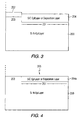
- FIGS. 2-4 illustrate another possible process to make a SiC die edge zone.
- a recessed edge zone 201 is etched by either a dry or a wet etch procedure to a specified depth in a silicon die 200, represented as an N-epitaxial layer, using an oxide mask 202 to prevent silicon removal from the active region 203, as shown in FIG. 2.
- a SiC layer 204 which is of the same conduction type as the epitaxial layer, is formed on recessed edge zone 201 using heteroepitaxial growth or deposition techniques, as shown in FIG. 3.
- Oxide mask 202 is then removed, and chemical-mechanical polishing (CMP) is performed to produce a fully planarized die 205 that includes SiC edge zone 204a having a selected thickness, as demonstrated in FIG. 4.
- CMP chemical-mechanical polishing
- Die 500 includes a substrate 501 bearing an N-epitaxial layer 502, in which is implanted a P-well 503. On the surface 504 of epitaxial layer 502 is deposited an oxide layer 505 and, in contact with P-well 503, a front metal layer 506 that is further in contact with a field plate 507. A back metal layer (not shown) is formed on the bottom of substrate 501.
- the highest electron-hole generation site 508 is located close to the intersection of the PN junction 509 between P-well 503 and N-epitaxial layer 502 and silicon upper surface 504. This is due to the termination of PN junction 509 to form a planar diffused junction having a finite curvature, which causes electric field crowding near upper surface 504 and leads to large impact ionization values at the die edges. Consequently, the breakdown occurs at junction termination edge 508 rather than in the parallel plane portion 510.
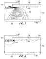
- Die 700 includes a substrate 701 bearing an N-epitaxial layer 702, in which is implanted a P-well 703.
- An oxide layer 706 is formed on SiC edge zone 705, and a front metal layer 707 interconnects P-well 703 with a field plate 708.
- a back metal layer (not shown) is formed on the bottom of substrate 701.
- FIGS. 7 and 8 illustrate the simulated avalanche leakage current and impact ionization contours, 709 and 710, respectively, for die 700.
- the breakdown location 710 is completely screened from the oxide layer 706 by SiC edge zone 705, and there is very little electron-hole generation along upper surface 704.
- the breakdown voltage for die 700 is higher than that observed for die 500.
- a prior art die 900 makes use of a deeper PN junction and thinner oxide to lower the curvature effect.
- Die 900 with field plate edge termination includes a substrate 901 bearing an N-epitaxial layer 902, in which is implanted a deep P-well 903.
- a thin oxide layer 905 On the surface 904 of epitaxial layer 902 is deposited a thin oxide layer 905 and, in contact with P-well 903, a front metal layer 906 that is further in contact with a field plate 907.
- a back metal layer (not shown) is formed on the bottom of substrate 901.
- FIGS. 9 and 10 illustrate the simulated avalanche leakage current and impact ionization contours, 908 and 911, respectively, for prior art die 900.
- the breakdown location is moved to the parallel plane portion 910 of PN junction 909.
- the device reliability of die 900 can be substantially improved .
- the avalanche breakdown location is shifted into the bulk silicon, there still exists a certain level of electron-hole generation along the interface 904 between epitaxial layer 902 and oxide layer 905.
- the simulation gives an impact ionization generation rate at breakdown location 911 of about 1x10 21 pairs/cm 3 .s and a generation rate at the same voltage of about 1x10 18 pairs/cm 3 .s at surface 904.
- Die 1100 includes a substrate 1101 bearing an N-epitaxial layer 1102, in which is implanted a P-well 1103. At the surface 1104 of epitaxial layer 1102 is formed a SiC edge zone 1105 that extends into N-epitaxial layer 1102 to a depth below that of P-well 1103. An oxide layer 1106 is formed on SiC edge zone 1105, and a front metal layer 1107 interconnects P-well 1103. Unlike previously described dies, die 1100 includes no field plate. A back metal layer (not shown) is formed on the bottom of substrate 1101.
- FIGS. 11 and 12 illustrate the simulated avalanche leakage current and impact ionization contours, 1110 and 1111, respectively, for die 1100 of the present invention.
- the breakdown location is optimally situated at P-N junction parallel plane portion 1109.
- the electron-hole generation at upper surface 1104 is extremely low.
- FIG. 13 a plot of impact ionization along the Si/SiO 2 interface versus distance from the P-N junction at the interface, depicts the surface carrier generation characteristics of the field plate-containing prior art dies 500 (cf. FIGS. 5,6) and 900 (cf. FIGS. 9,10) shown in FIGS. 5 and 9, along with die 1100 (cf. FIGS. 11, 12) of the present invention.
- the SiC edge termination included in die 1100 lowers the electron-hole avalanche generation rate more than 20 orders of magnitude compared with prior art die 500, and more than16 orders of magnitude compared with prior art die 900.
- the breakdown voltage of die 1100 is desirably increased as a result of the thicker net epitaxial layer, which is defined by the distance between the parallel plane portion 1109 of the PN junction and highly doped substrate 1101.
- Another improvement provided by the present invention is a reduction in edge termination area, which is controlled by the width of the surface depletion layer.
- Edge termination in accordance with the present invention does not change the curvature of the edge planar junction and the equal-potential contour distributions. Therefore the width of the surface depletion layer, which is less than the depletion width of the parallel plane portion, does change.
- the area of edge termination in die 1100 is expected to be about half that of the theoretical "ideal" Si edge termination.
- the width of the edge zone containing material with a higher critical electrical field than silicon can be chosen to be equal to the width of the surface depletion layer of the edge planar junction.
- the width of the SiC edge zone 1105 in die 1100 (cf. FIG. 12) is reduced to correspond to the surface depletion layer boundary 1112 of the PN junction 1109.
- the simulated breakdown characteristic does not change, and the breakdown voltage also remains the same.
- the depletion layer boundary 1112 of die 1100 at the onset of avalanche breakdown is shown in FIG. 14A.
- the depletion layer boundary 912 of field plate-containing die 900 (cf. FIG. 10) is depicted in FIG. 14B.
- the width of the depletion layer in prior art die 900 is at least two times greater than that of die 1100 of the present invention.
- edge termination of the present invention can be advantageously applied in semiconductor dies that include other edge terminating features such as, for example, field limiting rings (FLR), variable lateral doping concentration (VLD), and junction termination extension (JTE).
- FLR field limiting rings
- VLD variable lateral doping concentration
- JTE junction termination extension
- a silicon semiconductor die comprises a heavily doped silicon substrate and an upper layer comprising doped silicon of a first conduction type disposed on the substrate.
- the upper layer comprises a well region of a second, opposite conduction type adjacent an edge termination zone that comprises a layer of a material having a higher critical electric field than silicon. Both the well region and adjacent edge termination zone are disposed at an upper surface of the upper layer, and an oxide layer overlies the upper layer and the edge termination zone.
- a process for forming a silicon die having edge termination. The process comprises forming an upper layer comprising doped silicon of a first conduction type on a heavily doped silicon substrate, and forming an edge termination zone that comprises a layer of a material having a higher critical electric field than silicon at an upper surface of the upper layer.
- a well region of a second, opposite conduction type is formed at the upper surface of the upper layer adjacent the edge termination zone, and an oxide layer is formed over the upper layer and edge termination zone.
Landscapes
- Electrodes Of Semiconductors (AREA)
- Bipolar Transistors (AREA)
- Insulated Gate Type Field-Effect Transistor (AREA)
- Thyristors (AREA)
- Formation Of Insulating Films (AREA)
Claims (10)
- Silizium-Halbleiter-Die, umfassend ein stark dotiertes Siliziumsubstrat und eine obere Schicht (702, 1102), umfassend dotiertes Silizium einer ersten Art der Leitung, das auf dem Substrat angeordnet ist,
wobei die obere Schicht eine Quellregion (703, 1103) einer zweiten, entgegen gesetzten Art der Leitung umfasst, die einer Randabschlusszone (705, 1105) benachbart ist, wobei die Quellregion und die benachbarte Randabschlusszone, beide an der oberen Fläche der oberen Schicht angeordnet sind,
dadurch gekennzeichnet, dass eine Oxidschicht (706, 1106) auf der oberen Schicht und der Randabschlusszone aufliegt, wobei die Randabschlusszone eine Schicht eines Materials umfasst, das ein höheres kritisches elektrisches Feld als Silizium aufweist. - Die bzw. Rohchip gemäß Anspruch 1, dadurch gekennzeichnet, dass die obere Schicht eine epitaktische Schicht ist.
- Die gemäß Anspruch 1, dadurch gekennzeichnet, dass die Randabschlusszone eine Schicht aus Siliziumcarbid umfasst.
- Die gemäß Anspruch 1, dadurch gekennzeichnet, dass eine vordere Metallschicht aufliegt und im elektrischen Kontakt mit der Quellregion steht und eine hintere Metallschicht auf einer unteren Fläche des Substrats angeordnet ist und eine Feldplatte im elektrischen Kontakt mit der vorderen Metallschicht steht.
- Die gemäß Anspruch 1, dadurch gekennzeichnet, dass die Randabschlusszone eine gewählte Dicke aufweist und die Randabschlusszone in der oberen Schicht ausgespart ist und sich in die obere Schicht bis zu einer Tiefe erstreckt, die größer ist als die Tiefe der benachbarten Quellregion.
- Die gemäß Anspruch 1, der feldbegrenzende Ringe beinhaltet und auch eine variable laterale Dotierungskonzentration beinhaltet und weiter eine Übergangsabschlusserweiterung beinhaltet.
- Verfahren zum Bilden eines Silizium-Dies bzw. Rohchips mit einem verbesserten Randabschluss, wobei das Verfahren umfasst:Bilden einer oberen Schicht, umfassend dotiertes Silizium einer ersten Art der Leitung auf einem stark dotierten Siliziumsubstrat,Bilden an Randabschlusszone an einer oberen Fläche der oberen Schicht, wobei die Randabschlusszone eine Schicht eines Materials umfasst, das ein höheres kritisches elektrisches Feld als Silizium aufweist,Bilden einer Quellregion einer zweiten, entgegen gesetzten Art der Leitung in der oberen Schicht, die der Randabschlusszone benachbart ist, undBilden einer Oxidschicht über der oberen Schicht und der Randabschlusszone.
- Verfahren gemäß Anspruch 7, wobei die obere Schicht eine epitaktische Schicht ist, die erste Art der Leitung N ist und die zweite Art der Leitung P ist oder die erste Art der Leitung P ist und die zweite Art der Leitung N ist.
- Verfahren gemäß Anspruch 7, gekennzeichnet dadurch, dass die Randabschlusszone eine gewählte Dicke aufweist, und wobei die Randabschlusszone eine Schicht aus Siliziumcarbid umfasst, bei dem das Bilden der Schicht aus Siliziumcarbid ein Implantieren, ein Aktivieren und ein Diffundieren von Kohlenstoff in die obere Silizium-Schicht umfasst.
- Verfahren gemäß Anspruch 7, dadurch gekennzeichnet, dass das Bilden der Randabschlusszone ein Ätzen der oberen Fläche der oberen Schicht vor dem Bilden der Schicht aus Siliziumcarbid umfasst, wodurch eine Randabschlusszone bereitgestellt wird, die in der oberen Schicht ausgespart ist, bei dem sich die Randabschlusszone, die in der oberen Schicht ausgespart ist, in die obere Schicht bis zu einer Tiefe erstreckt, die größer ist als die Tiefe der benachbarten Quellregion.
Applications Claiming Priority (2)
| Application Number | Priority Date | Filing Date | Title |
|---|---|---|---|
| US344868 | 1999-06-28 | ||
| US09/344,868 US6242784B1 (en) | 1999-06-28 | 1999-06-28 | Edge termination for silicon power devices |
Publications (3)
| Publication Number | Publication Date |
|---|---|
| EP1065727A2 EP1065727A2 (de) | 2001-01-03 |
| EP1065727A3 EP1065727A3 (de) | 2003-05-02 |
| EP1065727B1 true EP1065727B1 (de) | 2006-05-24 |
Family
ID=23352402
Family Applications (1)
| Application Number | Title | Priority Date | Filing Date |
|---|---|---|---|
| EP00401826A Expired - Lifetime EP1065727B1 (de) | 1999-06-28 | 2000-06-27 | Randabschluss für Silizium-Leistungsanordnungen |
Country Status (5)
| Country | Link |
|---|---|
| US (5) | US6242784B1 (de) |
| EP (1) | EP1065727B1 (de) |
| JP (1) | JP4955139B2 (de) |
| KR (1) | KR100619621B1 (de) |
| DE (1) | DE60028134T2 (de) |
Families Citing this family (41)
| Publication number | Priority date | Publication date | Assignee | Title |
|---|---|---|---|---|
| DE69938541D1 (de) * | 1999-06-03 | 2008-05-29 | St Microelectronics Srl | Leistungshalbleiteranordnung mit einer Randabschlussstruktur mit einem Spannungsteiler |
| US6242784B1 (en) * | 1999-06-28 | 2001-06-05 | Intersil Corporation | Edge termination for silicon power devices |
| DE19942679C1 (de) * | 1999-09-07 | 2001-04-05 | Infineon Technologies Ag | Verfahren zum Herstellen eines hochvolttauglichen Randabschlusses bei einem nach dem Prinzip der lateralen Ladungskompensation vorgefertigten Grundmaterialwafer |
| JP3667676B2 (ja) * | 2001-10-11 | 2005-07-06 | 株式会社東芝 | 半導体装置、半導体装置の製造方法及び半導体装置の電気特性評価システム |
| US6825510B2 (en) | 2002-09-19 | 2004-11-30 | Fairchild Semiconductor Corporation | Termination structure incorporating insulator in a trench |
| US6818947B2 (en) | 2002-09-19 | 2004-11-16 | Fairchild Semiconductor Corporation | Buried gate-field termination structure |
| US7026650B2 (en) * | 2003-01-15 | 2006-04-11 | Cree, Inc. | Multiple floating guard ring edge termination for silicon carbide devices |
| US9515135B2 (en) * | 2003-01-15 | 2016-12-06 | Cree, Inc. | Edge termination structures for silicon carbide devices |
| US7638841B2 (en) | 2003-05-20 | 2009-12-29 | Fairchild Semiconductor Corporation | Power semiconductor devices and methods of manufacture |
| US7618880B1 (en) * | 2004-02-19 | 2009-11-17 | Quick Nathaniel R | Apparatus and method for transformation of substrate |
| WO2005119793A2 (en) * | 2004-05-28 | 2005-12-15 | Caracal, Inc. | Silicon carbide schottky diodes and fabrication method |
| US7304363B1 (en) * | 2004-11-26 | 2007-12-04 | United States Of America As Represented By The Secretary Of The Army | Interacting current spreader and junction extender to increase the voltage blocked in the off state of a high power semiconductor device |
| US20060197153A1 (en) * | 2005-02-23 | 2006-09-07 | Chih-Feng Huang | Vertical transistor with field region structure |
| DE102005023668B3 (de) * | 2005-05-23 | 2006-11-09 | Infineon Technologies Ag | Halbleiterbauelement mit einer Randstruktur mit Spannungsdurchbruch im linearen Bereich |
| US7525122B2 (en) * | 2005-06-29 | 2009-04-28 | Cree, Inc. | Passivation of wide band-gap based semiconductor devices with hydrogen-free sputtered nitrides |
| US7598576B2 (en) * | 2005-06-29 | 2009-10-06 | Cree, Inc. | Environmentally robust passivation structures for high-voltage silicon carbide semiconductor devices |
| US7855401B2 (en) * | 2005-06-29 | 2010-12-21 | Cree, Inc. | Passivation of wide band-gap based semiconductor devices with hydrogen-free sputtered nitrides |
| DE112006002377B4 (de) * | 2005-09-08 | 2014-04-24 | Mitsubishi Denki K.K. | Halbleitervorrichtung und Verfahren zum Herstellen einer Halbleitervorrichtung |
| DE102005056426B4 (de) * | 2005-11-28 | 2012-03-15 | Infineon Technologies Austria Ag | Halbleiterbauelement und Verfahren zu dessen Herstellung |
| US7541660B2 (en) * | 2006-04-20 | 2009-06-02 | Infineon Technologies Austria Ag | Power semiconductor device |
| US7579650B2 (en) * | 2006-08-09 | 2009-08-25 | International Rectifier Corporation | Termination design for deep source electrode MOSFET |
| US8110888B2 (en) * | 2007-09-18 | 2012-02-07 | Microsemi Corporation | Edge termination for high voltage semiconductor device |
| CN101868856B (zh) | 2007-09-21 | 2014-03-12 | 飞兆半导体公司 | 用于功率器件的超结结构及制造方法 |
| US8174067B2 (en) * | 2008-12-08 | 2012-05-08 | Fairchild Semiconductor Corporation | Trench-based power semiconductor devices with increased breakdown voltage characteristics |
| US8304829B2 (en) | 2008-12-08 | 2012-11-06 | Fairchild Semiconductor Corporation | Trench-based power semiconductor devices with increased breakdown voltage characteristics |
| US8106487B2 (en) | 2008-12-23 | 2012-01-31 | Pratt & Whitney Rocketdyne, Inc. | Semiconductor device having an inorganic coating layer applied over a junction termination extension |
| US8227855B2 (en) * | 2009-02-09 | 2012-07-24 | Fairchild Semiconductor Corporation | Semiconductor devices with stable and controlled avalanche characteristics and methods of fabricating the same |
| US8148749B2 (en) * | 2009-02-19 | 2012-04-03 | Fairchild Semiconductor Corporation | Trench-shielded semiconductor device |
| US8049276B2 (en) * | 2009-06-12 | 2011-11-01 | Fairchild Semiconductor Corporation | Reduced process sensitivity of electrode-semiconductor rectifiers |
| JP5658464B2 (ja) * | 2010-02-03 | 2015-01-28 | キヤノン株式会社 | 画像読取装置、及びその制御方法 |
| US8389348B2 (en) * | 2010-09-14 | 2013-03-05 | Taiwan Semiconductor Manufacturing Company, Ltd. | Mechanism of forming SiC crystalline on Si substrates to allow integration of GaN and Si electronics |
| US8872278B2 (en) | 2011-10-25 | 2014-10-28 | Fairchild Semiconductor Corporation | Integrated gate runner and field implant termination for trench devices |
| US9178013B2 (en) | 2012-02-06 | 2015-11-03 | Infineon Technologies Austria Ag | Semiconductor device with edge termination and method for manufacturing a semiconductor device |
| DE112012005981B4 (de) | 2012-03-05 | 2025-04-30 | Mitsubishi Electric Corporation | Halbleitervorrichtungen |
| US9991399B2 (en) | 2012-10-04 | 2018-06-05 | Cree, Inc. | Passivation structure for semiconductor devices |
| US9812338B2 (en) | 2013-03-14 | 2017-11-07 | Cree, Inc. | Encapsulation of advanced devices using novel PECVD and ALD schemes |
| US8994073B2 (en) | 2012-10-04 | 2015-03-31 | Cree, Inc. | Hydrogen mitigation schemes in the passivation of advanced devices |
| US9082843B2 (en) | 2012-12-13 | 2015-07-14 | Infineon Technologies Ag | Semiconductor device with step-shaped edge termination, and method for manufacturing a semiconductor device |
| WO2017009061A1 (en) | 2015-07-10 | 2017-01-19 | BASF Agro B.V. | Herbicidal composition comprising cinmethylin and saflufenacil |
| CN112310188A (zh) * | 2019-07-23 | 2021-02-02 | 珠海格力电器股份有限公司 | 横向变掺杂终端结构及其制造方法 |
| CN114613845B (zh) * | 2022-03-17 | 2025-08-05 | 江苏铨力微电子有限公司 | 一种高压mosfet晶体管终端结构及制备方法 |
Citations (2)
| Publication number | Priority date | Publication date | Assignee | Title |
|---|---|---|---|---|
| US5489799A (en) * | 1993-07-01 | 1996-02-06 | Consorzio Per La Ricerca Sulla Microelecttronica Nel Mezzogiorno | Integrated edge structure for high voltage semiconductor devices and related manufacturing processs |
| EP0768714A1 (de) * | 1995-10-09 | 1997-04-16 | Consorzio per la Ricerca sulla Microelettronica nel Mezzogiorno - CoRiMMe | Herstellungsverfahren für Leistungsanordnung mit Schutzring |
Family Cites Families (10)
| Publication number | Priority date | Publication date | Assignee | Title |
|---|---|---|---|---|
| US4374389A (en) * | 1978-06-06 | 1983-02-15 | General Electric Company | High breakdown voltage semiconductor device |
| JPS58192368A (ja) * | 1982-05-07 | 1983-11-09 | Toshiba Corp | 高耐圧プレ−ナ型半導体装置 |
| JPH06275852A (ja) * | 1993-03-18 | 1994-09-30 | Hitachi Ltd | 高耐圧半導体装置 |
| JP3185474B2 (ja) * | 1993-05-18 | 2001-07-09 | 株式会社日立製作所 | 半導体装置 |
| US5510275A (en) * | 1993-11-29 | 1996-04-23 | Texas Instruments Incorporated | Method of making a semiconductor device with a composite drift region composed of a substrate and a second semiconductor material |
| TW286435B (de) * | 1994-07-27 | 1996-09-21 | Siemens Ag | |
| JP3327135B2 (ja) * | 1996-09-09 | 2002-09-24 | 日産自動車株式会社 | 電界効果トランジスタ |
| SE9700156D0 (sv) * | 1997-01-21 | 1997-01-21 | Abb Research Ltd | Junction termination for Si C Schottky diode |
| JP3958404B2 (ja) * | 1997-06-06 | 2007-08-15 | 三菱電機株式会社 | 横型高耐圧素子を有する半導体装置 |
| US6242784B1 (en) * | 1999-06-28 | 2001-06-05 | Intersil Corporation | Edge termination for silicon power devices |
-
1999
- 1999-06-28 US US09/344,868 patent/US6242784B1/en not_active Expired - Lifetime
-
2000
- 2000-06-20 JP JP2000184291A patent/JP4955139B2/ja not_active Expired - Fee Related
- 2000-06-27 DE DE60028134T patent/DE60028134T2/de not_active Expired - Lifetime
- 2000-06-27 EP EP00401826A patent/EP1065727B1/de not_active Expired - Lifetime
- 2000-06-28 KR KR1020000036216A patent/KR100619621B1/ko not_active Expired - Fee Related
-
2001
- 2001-02-23 US US09/792,345 patent/US6534347B2/en not_active Expired - Lifetime
- 2001-03-23 US US09/815,672 patent/US6362026B2/en not_active Expired - Lifetime
-
2002
- 2002-12-20 US US10/327,443 patent/US6759719B2/en not_active Expired - Fee Related
-
2004
- 2004-07-02 US US10/882,387 patent/US7166866B2/en not_active Expired - Lifetime
Patent Citations (2)
| Publication number | Priority date | Publication date | Assignee | Title |
|---|---|---|---|---|
| US5489799A (en) * | 1993-07-01 | 1996-02-06 | Consorzio Per La Ricerca Sulla Microelecttronica Nel Mezzogiorno | Integrated edge structure for high voltage semiconductor devices and related manufacturing processs |
| EP0768714A1 (de) * | 1995-10-09 | 1997-04-16 | Consorzio per la Ricerca sulla Microelettronica nel Mezzogiorno - CoRiMMe | Herstellungsverfahren für Leistungsanordnung mit Schutzring |
Non-Patent Citations (1)
| Title |
|---|
| SKORUPA ET AL: "carbon-mediated effects in silicon and in silicon-related materials", MATERIALS INDUSTRY AND PHYSICS, vol. 44, 1996, pages 101 - 144, XP000916720 * |
Also Published As
| Publication number | Publication date |
|---|---|
| US20040238903A1 (en) | 2004-12-02 |
| US6362026B2 (en) | 2002-03-26 |
| KR100619621B1 (ko) | 2006-09-06 |
| DE60028134D1 (de) | 2006-06-29 |
| US20010007369A1 (en) | 2001-07-12 |
| DE60028134T2 (de) | 2007-03-15 |
| US20030127693A1 (en) | 2003-07-10 |
| EP1065727A3 (de) | 2003-05-02 |
| US6534347B2 (en) | 2003-03-18 |
| US6759719B2 (en) | 2004-07-06 |
| US6242784B1 (en) | 2001-06-05 |
| US7166866B2 (en) | 2007-01-23 |
| JP4955139B2 (ja) | 2012-06-20 |
| EP1065727A2 (de) | 2001-01-03 |
| KR20010029855A (ko) | 2001-04-16 |
| JP2001036085A (ja) | 2001-02-09 |
| US20010050369A1 (en) | 2001-12-13 |
Similar Documents
| Publication | Publication Date | Title |
|---|---|---|
| EP1065727B1 (de) | Randabschluss für Silizium-Leistungsanordnungen | |
| US11961904B2 (en) | Semiconductor device including trench gate structure and buried shielding region and method of manufacturing | |
| JP6640904B2 (ja) | トレンチ下部にオフセットを有するSiC半導体デバイス | |
| US8258032B2 (en) | Power semiconductor devices and methods for manufacturing the same | |
| EP1845561B1 (de) | Halbleiterbauelement mit einer Heteroübergang Diode und Herstellungsverfahren dafür | |
| US5747831A (en) | SIC field-effect transistor array with ring type trenches and method of producing them | |
| CA2195987C (en) | Semiconductor component with junction termination with high blocking effectiveness | |
| EP0840943B1 (de) | Durchbruchtransierter niederspannungs-unterdrücker mit zweischichtiger basis | |
| US6215168B1 (en) | Doubly graded junction termination extension for edge passivation of semiconductor devices | |
| EP1016142B1 (de) | SiC HALBLEITERBAUELEMENT MIT EINEM PN-ÜBERGANG | |
| EP3552239A1 (de) | Leistungshalbleiterbauelemente mit gate-gräben und eingelassenen abschlussstrukturen sowie zugehörige verfahren | |
| EP1485940B1 (de) | Siliziumcarbid-bipolar-sperrschichttransistor mit überwachsener basisregion | |
| US11615953B2 (en) | Silicon carbide semiconductor device with a contact region having edges recessed from edges of the well region | |
| US7154177B2 (en) | Semiconductor device with edge structure | |
| JP2003101022A (ja) | 電力用半導体素子 | |
| US9978832B1 (en) | Wide bandgap semiconductor device with vertical superjunction edge termination for the drift region | |
| WO2023219792A1 (en) | Vertical power devices having mesas and etched trenches therebetween |
Legal Events
| Date | Code | Title | Description |
|---|---|---|---|
| PUAI | Public reference made under article 153(3) epc to a published international application that has entered the european phase |
Free format text: ORIGINAL CODE: 0009012 |
|
| AK | Designated contracting states |
Kind code of ref document: A2 Designated state(s): AT BE CH CY DE DK ES FI FR GB GR IE IT LI LU MC NL PT SE |
|
| AX | Request for extension of the european patent |
Free format text: AL;LT;LV;MK;RO;SI |
|
| PUAL | Search report despatched |
Free format text: ORIGINAL CODE: 0009013 |
|
| AK | Designated contracting states |
Designated state(s): AT BE CH CY DE DK ES FI FR GB GR IE IT LI LU MC NL PT SE |
|
| AX | Request for extension of the european patent |
Extension state: AL LT LV MK RO SI |
|
| 17P | Request for examination filed |
Effective date: 20031016 |
|
| AKX | Designation fees paid |
Designated state(s): DE FR GB IT SE |
|
| 17Q | First examination report despatched |
Effective date: 20041115 |
|
| GRAP | Despatch of communication of intention to grant a patent |
Free format text: ORIGINAL CODE: EPIDOSNIGR1 |
|
| GRAS | Grant fee paid |
Free format text: ORIGINAL CODE: EPIDOSNIGR3 |
|
| GRAA | (expected) grant |
Free format text: ORIGINAL CODE: 0009210 |
|
| AK | Designated contracting states |
Kind code of ref document: B1 Designated state(s): DE FR GB IT SE |
|
| REG | Reference to a national code |
Ref country code: GB Ref legal event code: FG4D |
|
| REF | Corresponds to: |
Ref document number: 60028134 Country of ref document: DE Date of ref document: 20060629 Kind code of ref document: P |
|
| PG25 | Lapsed in a contracting state [announced via postgrant information from national office to epo] |
Ref country code: SE Free format text: LAPSE BECAUSE OF FAILURE TO SUBMIT A TRANSLATION OF THE DESCRIPTION OR TO PAY THE FEE WITHIN THE PRESCRIBED TIME-LIMIT Effective date: 20060824 |
|
| ET | Fr: translation filed | ||
| PLBE | No opposition filed within time limit |
Free format text: ORIGINAL CODE: 0009261 |
|
| STAA | Information on the status of an ep patent application or granted ep patent |
Free format text: STATUS: NO OPPOSITION FILED WITHIN TIME LIMIT |
|
| GBPC | Gb: european patent ceased through non-payment of renewal fee |
Effective date: 20060824 |
|
| 26N | No opposition filed |
Effective date: 20070227 |
|
| PG25 | Lapsed in a contracting state [announced via postgrant information from national office to epo] |
Ref country code: GB Free format text: LAPSE BECAUSE OF NON-PAYMENT OF DUE FEES Effective date: 20060824 |
|
| PGFP | Annual fee paid to national office [announced via postgrant information from national office to epo] |
Ref country code: DE Payment date: 20130627 Year of fee payment: 14 |
|
| PGFP | Annual fee paid to national office [announced via postgrant information from national office to epo] |
Ref country code: FR Payment date: 20130702 Year of fee payment: 14 Ref country code: IT Payment date: 20130625 Year of fee payment: 14 |
|
| REG | Reference to a national code |
Ref country code: DE Ref legal event code: R119 Ref document number: 60028134 Country of ref document: DE |
|
| REG | Reference to a national code |
Ref country code: DE Ref legal event code: R119 Ref document number: 60028134 Country of ref document: DE Effective date: 20150101 |
|
| REG | Reference to a national code |
Ref country code: FR Ref legal event code: ST Effective date: 20150227 |
|
| PG25 | Lapsed in a contracting state [announced via postgrant information from national office to epo] |
Ref country code: IT Free format text: LAPSE BECAUSE OF NON-PAYMENT OF DUE FEES Effective date: 20140627 Ref country code: DE Free format text: LAPSE BECAUSE OF NON-PAYMENT OF DUE FEES Effective date: 20150101 |
|
| PG25 | Lapsed in a contracting state [announced via postgrant information from national office to epo] |
Ref country code: FR Free format text: LAPSE BECAUSE OF NON-PAYMENT OF DUE FEES Effective date: 20140630 |