EP1065913A2 - Bestrahlendes Heizelement aus pyrolytischem Bornitrid - Google Patents
Bestrahlendes Heizelement aus pyrolytischem Bornitrid Download PDFInfo
- Publication number
- EP1065913A2 EP1065913A2 EP00401406A EP00401406A EP1065913A2 EP 1065913 A2 EP1065913 A2 EP 1065913A2 EP 00401406 A EP00401406 A EP 00401406A EP 00401406 A EP00401406 A EP 00401406A EP 1065913 A2 EP1065913 A2 EP 1065913A2
- Authority
- EP
- European Patent Office
- Prior art keywords
- boron nitride
- pyrolytic
- outer coating
- pyrolytic boron
- heating element
- Prior art date
- Legal status (The legal status is an assumption and is not a legal conclusion. Google has not performed a legal analysis and makes no representation as to the accuracy of the status listed.)
- Withdrawn
Links
Images

Classifications
-
- C—CHEMISTRY; METALLURGY
- C23—COATING METALLIC MATERIAL; COATING MATERIAL WITH METALLIC MATERIAL; CHEMICAL SURFACE TREATMENT; DIFFUSION TREATMENT OF METALLIC MATERIAL; COATING BY VACUUM EVAPORATION, BY SPUTTERING, BY ION IMPLANTATION OR BY CHEMICAL VAPOUR DEPOSITION, IN GENERAL; INHIBITING CORROSION OF METALLIC MATERIAL OR INCRUSTATION IN GENERAL
- C23C—COATING METALLIC MATERIAL; COATING MATERIAL WITH METALLIC MATERIAL; SURFACE TREATMENT OF METALLIC MATERIAL BY DIFFUSION INTO THE SURFACE, BY CHEMICAL CONVERSION OR SUBSTITUTION; COATING BY VACUUM EVAPORATION, BY SPUTTERING, BY ION IMPLANTATION OR BY CHEMICAL VAPOUR DEPOSITION, IN GENERAL
- C23C16/00—Chemical coating by decomposition of gaseous compounds, without leaving reaction products of surface material in the coating, i.e. chemical vapour deposition [CVD] processes
-
- H—ELECTRICITY
- H05—ELECTRIC TECHNIQUES NOT OTHERWISE PROVIDED FOR
- H05B—ELECTRIC HEATING; ELECTRIC LIGHT SOURCES NOT OTHERWISE PROVIDED FOR; CIRCUIT ARRANGEMENTS FOR ELECTRIC LIGHT SOURCES, IN GENERAL
- H05B3/00—Ohmic-resistance heating
- H05B3/10—Heating elements characterised by the composition or nature of the materials or by the arrangement of the conductor
- H05B3/12—Heating elements characterised by the composition or nature of the materials or by the arrangement of the conductor characterised by the composition or nature of the conductive material
- H05B3/14—Heating elements characterised by the composition or nature of the materials or by the arrangement of the conductor characterised by the composition or nature of the conductive material the material being non-metallic
- H05B3/141—Conductive ceramics, e.g. metal oxides, metal carbides, barium titanate, ferrites, zirconia, vitrous compounds
-
- H—ELECTRICITY
- H05—ELECTRIC TECHNIQUES NOT OTHERWISE PROVIDED FOR
- H05B—ELECTRIC HEATING; ELECTRIC LIGHT SOURCES NOT OTHERWISE PROVIDED FOR; CIRCUIT ARRANGEMENTS FOR ELECTRIC LIGHT SOURCES, IN GENERAL
- H05B3/00—Ohmic-resistance heating
- H05B3/10—Heating elements characterised by the composition or nature of the materials or by the arrangement of the conductor
- H05B3/12—Heating elements characterised by the composition or nature of the materials or by the arrangement of the conductor characterised by the composition or nature of the conductive material
- H05B3/14—Heating elements characterised by the composition or nature of the materials or by the arrangement of the conductor characterised by the composition or nature of the conductive material the material being non-metallic
- H05B3/141—Conductive ceramics, e.g. metal oxides, metal carbides, barium titanate, ferrites, zirconia, vitrous compounds
- H05B3/143—Conductive ceramics, e.g. metal oxides, metal carbides, barium titanate, ferrites, zirconia, vitrous compounds applied to semiconductors, e.g. wafers heating
-
- H—ELECTRICITY
- H05—ELECTRIC TECHNIQUES NOT OTHERWISE PROVIDED FOR
- H05B—ELECTRIC HEATING; ELECTRIC LIGHT SOURCES NOT OTHERWISE PROVIDED FOR; CIRCUIT ARRANGEMENTS FOR ELECTRIC LIGHT SOURCES, IN GENERAL
- H05B3/00—Ohmic-resistance heating
- H05B3/10—Heating elements characterised by the composition or nature of the materials or by the arrangement of the conductor
- H05B3/12—Heating elements characterised by the composition or nature of the materials or by the arrangement of the conductor characterised by the composition or nature of the conductive material
- H05B3/14—Heating elements characterised by the composition or nature of the materials or by the arrangement of the conductor characterised by the composition or nature of the conductive material the material being non-metallic
- H05B3/145—Carbon only, e.g. carbon black, graphite
-
- H—ELECTRICITY
- H05—ELECTRIC TECHNIQUES NOT OTHERWISE PROVIDED FOR
- H05B—ELECTRIC HEATING; ELECTRIC LIGHT SOURCES NOT OTHERWISE PROVIDED FOR; CIRCUIT ARRANGEMENTS FOR ELECTRIC LIGHT SOURCES, IN GENERAL
- H05B3/00—Ohmic-resistance heating
- H05B3/20—Heating elements having extended surface area substantially in a two-dimensional [2D] plane, e.g. plate-heater
- H05B3/22—Heating elements having extended surface area substantially in a two-dimensional [2D] plane, e.g. plate-heater non-flexible
- H05B3/26—Heating elements having extended surface area substantially in a two-dimensional [2D] plane, e.g. plate-heater non-flexible heating conductor mounted on insulating base
- H05B3/265—Heating elements having extended surface area substantially in a two-dimensional [2D] plane, e.g. plate-heater non-flexible heating conductor mounted on insulating base the insulating base being an inorganic material, e.g. ceramic
-
- H—ELECTRICITY
- H05—ELECTRIC TECHNIQUES NOT OTHERWISE PROVIDED FOR
- H05B—ELECTRIC HEATING; ELECTRIC LIGHT SOURCES NOT OTHERWISE PROVIDED FOR; CIRCUIT ARRANGEMENTS FOR ELECTRIC LIGHT SOURCES, IN GENERAL
- H05B3/00—Ohmic-resistance heating
- H05B3/20—Heating elements having extended surface area substantially in a two-dimensional [2D] plane, e.g. plate-heater
- H05B3/22—Heating elements having extended surface area substantially in a two-dimensional [2D] plane, e.g. plate-heater non-flexible
- H05B3/28—Heating elements having extended surface area substantially in a two-dimensional [2D] plane, e.g. plate-heater non-flexible heating conductor embedded in insulating material
- H05B3/283—Heating elements having extended surface area substantially in a two-dimensional [2D] plane, e.g. plate-heater non-flexible heating conductor embedded in insulating material the insulating material being an inorganic material, e.g. ceramic
Definitions
- This invention relates to pyrolytic boron nitride heating devices and more particularly to a pyrolytic boron nitride radiation heater.
- a pyrolytic boron nitride heating unit includes a dielectric body of boron nitride and a heating element contained within the boron nitride body.
- the heating element is composed of a conductive material preferably of graphite and more particularly pyrolytic graphite.
- a pyrolytic boron nitride heating unit may be fabricated by depositing a layer of a conductive heating material over a substrate of pyrolytic boron nitride over which is deposited an outer layer of pyrolytic boron nitride as taught in US Patent No. 5,343,022 the disclosure of which is herein incorporated by reference.
- the outer layer of pyrolytic boron nitride electrically insulates the surface of the heating element and provides protection to the heating element from mechanical damage.
- the heating element is connected to a power supply causing electricity to pass through the conductive material which, in turn, generates thermal energy by resistive heating.
- heat transfer is accomplished by conduction when the member or device to be heated is placed in physical contact with the heating element. It is, however, not always practical or even possible to establish physical contact between the heating element and the device or member to be heated. In these instances heat transfer must be accomplished by either convection or radiation.
- MBE molecular beam epitaxy
- MBE molecular beam epitaxy
- the semiconductor film is grown in a relatively high vacuum environment where heat transfer by convection is not possible and heat transfer by conduction is not practical. Accordingly, in this application, which is only one of many, radiation is the only available heat transfer mechanism.
- the efficiency of the heating unit to transmit thermal energy by radiation is directly proportional to the emissivity of the heating element in the heating unit.
- the emissivity of the heating element is defined as the ratio of the emissive power of an actual surface of the heating element to the emissive power of an ideal black body at the same temperature.
- the emissivity of commercially available pyrolytic boron nitride heating units has been measured at 0.55 at a wavelength of 1.55 microns. For purposes of comparison an ideal black body at the same wavelength would have a radiation thermal efficiency of 100% representing a measurement of 1.00. Accordingly, commercially available pyrolytic boron nitride heating units are not very efficient for use as radiant heaters.
- a pyrolytic boron nitride radiation heating unit has been developed in accordance with the present invention having a radiation efficiency above 80% and preferably above at least 85%.
- the pyrolytic boron nitride radiation heating unit of the present invention comprises a dielectric base of boron nitride, a heating element of pyrolytic graphite superimposed on the dielectric base, with the heating element having a geometry forming a pair of contact ends, a first outer coating surrounding said heating element composed of pyrolytic boron nitride and a second outer coating surrounding said first outer coating with said second outer coating selected from the group consisting of silicon carbide and boron carbide with said contact ends of said heating element extending through said first and second outer coating for forming contact terminals for said heating unit.
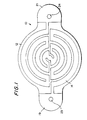
- the pyrolytic boron nitride heating unit 10 of the present invention as shown in Figures 1 and 2 (a-c) inclusive comprises a pyrolytic boron nitride base plate 12, a coated layer of pyrolytic graphite 14, a first overcoat layer of pyrolytic boron nitride 16 and a second overcoat layer of either silicon carbide or boron carbide 18.
- Pyrolytic boron nitride (PBN) is formed by chemical vapor deposition of boron nitride in a reactor chamber by the vapor phase reaction of ammonia and a boron containing gas such as boron trichloride (BCl 3 ) as more specifically described in US Patent 3,152,006.
- the pyrolytic boron nitride when separated from the substrate forms a self standing article of purified pyrolytic boron nitride.
- the thickness of the pyrolytic boron nitride base plate 12 is not critical to the subject invention.
- the base plate 12 may be configured into any desired geometry. In Figure 1 the base plate 12 is configured into a substantially circular geometry with two tabular ends 19 and 21 repectively.
- the pyrolytic graphite layer 14 is coated directly over the base plate 12 and forms the heating element in the pyrolytic boron nitride heating unit 10 upon connection to an external power supply (not shown).
- any conductive material can be used graphite and more particularly pyrolytic graphite is preferred.
- Pyrolytic graphite may be formed by chemical vapor deposition of, for example, methane gas at a very high temperature in a reactor chamber with a suitable inert diluent. The coating of pyrolytic graphite 14 is machined into a desired configuration to maximize the generation of heat.
- the pyrolytic graphite 14 conductor is machined into a continuous strip preferably forming a spiral or serpendine geometry extending from one tabular end 19 to the other tabular end 21 of the heating unit 10.
- the external power supply (not shown) is connected between the two tabular ends 19 and 21 preferably by piercing each of the tabular ends 19 and 21 to form holes 23 and 24 over which the pyrolytic graphite layer 14 is formed.
- the holes 23 and 24 are masked during the formation of the first and second overcoat layers 16 and 18 respectively so to provide access to the machined strip of pyrolytic graphite 14 through the holes 23 and 24.
- the first overcoat layer of pyrolytic boron nitride 16 is formed by chemical vapor deposition similar to the formation of the base plate 12 and encloses the pyrolytic graphite layer 14 except for the connections at the tabular ends 19 and 21.
- the first coating insulates and protects the conductive layer 14 from mechanical damage.
- a second outercoating 18 of silicon carbide or boron carbide is formed over the entire body except for the connections at the tabular ends 19 and 21.
- the second outercoating 18 may also be formed by chemical vapor deposition.
- the second outercoating 18 enhances the emissivity of the heating unit 10 for use as a radiation heater. With a coating of silicon carbide the emissivity of the heating unit 10 has been measured at 0.92 for a wavelength of 1.55.
- a coating of boron carbide will also provide a significant emissivity somewhat comparable to the emissivity of silicon carbide and sufficent to provide a radiation efficiency of above at least about 80% and preferably above 85%.
- the heating unit 10 is provided with an outer overcoat 18 with an emissivity such that the radiation efficiency is above 80% the rate of heat transfer is increased. This reduces the preheating time for heating a substrate.
Landscapes
- Chemical & Material Sciences (AREA)
- Engineering & Computer Science (AREA)
- Ceramic Engineering (AREA)
- Inorganic Chemistry (AREA)
- General Chemical & Material Sciences (AREA)
- Chemical Kinetics & Catalysis (AREA)
- Materials Engineering (AREA)
- Mechanical Engineering (AREA)
- Metallurgy (AREA)
- Organic Chemistry (AREA)
- Resistance Heating (AREA)
- Chemical Vapour Deposition (AREA)
- Ceramic Products (AREA)
Applications Claiming Priority (2)
| Application Number | Priority Date | Filing Date | Title |
|---|---|---|---|
| US347335 | 1999-07-02 | ||
| US09/347,335 US6140624A (en) | 1999-07-02 | 1999-07-02 | Pyrolytic boron nitride radiation heater |
Publications (2)
| Publication Number | Publication Date |
|---|---|
| EP1065913A2 true EP1065913A2 (de) | 2001-01-03 |
| EP1065913A3 EP1065913A3 (de) | 2001-08-08 |
Family
ID=23363282
Family Applications (1)
| Application Number | Title | Priority Date | Filing Date |
|---|---|---|---|
| EP00401406A Withdrawn EP1065913A3 (de) | 1999-07-02 | 2000-05-22 | Bestrahlendes Heizelement aus pyrolytischem Bornitrid |
Country Status (4)
| Country | Link |
|---|---|
| US (1) | US6140624A (de) |
| EP (1) | EP1065913A3 (de) |
| JP (1) | JP2001023759A (de) |
| KR (1) | KR20010014985A (de) |
Cited By (3)
| Publication number | Priority date | Publication date | Assignee | Title |
|---|---|---|---|---|
| EP1119025A3 (de) * | 2000-01-20 | 2006-05-17 | Sumitomo Electric Industries, Ltd. | Waferhalter für eine Halbleiterherstellungsvorrichtung |
| WO2009106942A1 (en) * | 2008-02-27 | 2009-09-03 | S.O.I.T.E.C Silicon On Insulator Technologies | Semiconductor growth system which includes a boron carbide reactor component |
| WO2009108221A3 (en) * | 2008-02-27 | 2010-07-22 | S.O.I.Tec Silicon On Insulator Technologies | Thermalization of gaseous precursors in cvd reactors |
Families Citing this family (14)
| Publication number | Priority date | Publication date | Assignee | Title |
|---|---|---|---|---|
| JP3963788B2 (ja) * | 2002-06-20 | 2007-08-22 | 信越化学工業株式会社 | 静電吸着機能を有する加熱装置 |
| US20040074898A1 (en) * | 2002-10-21 | 2004-04-22 | Mariner John T. | Encapsulated graphite heater and process |
| CN1954095B (zh) * | 2004-07-05 | 2010-06-09 | 东京毅力科创株式会社 | 处理装置和加热器单元 |
| BRPI0516136A (pt) | 2004-09-27 | 2008-08-26 | Gallium Entpr Pty Ltd | método e equipamento para desenvolvimento de uma pelìcula de nitreto de um metal do grupo (iii) e a pelìcula de nitreto do metal do grupo (iii) |
| US20070181065A1 (en) * | 2006-02-09 | 2007-08-09 | General Electric Company | Etch resistant heater and assembly thereof |
| US7741584B2 (en) * | 2007-01-21 | 2010-06-22 | Momentive Performance Materials Inc. | Encapsulated graphite heater and process |
| JP2011225949A (ja) * | 2010-04-21 | 2011-11-10 | Ibiden Co Ltd | 炭素部品および炭素部品の製造方法 |
| CN107335121B (zh) * | 2011-06-16 | 2022-06-03 | 瑞思迈私人有限公司 | 加湿器和层式加热元件 |
| US8763161B2 (en) | 2012-02-10 | 2014-06-24 | The United States of America, as represented by the Secretary of Commerce, The National Institute of Standards and Technology | Zero thermal expansion, low heat transfer, variable temperature sample assembly for probe microscopy |
| CN105379415A (zh) * | 2013-07-15 | 2016-03-02 | 莫门蒂夫性能材料股份有限公司 | 带涂层的石墨加热器构造 |
| US10679873B2 (en) * | 2016-09-30 | 2020-06-09 | Ngk Spark Plug Co., Ltd. | Ceramic heater |
| CN110572889B (zh) * | 2019-10-21 | 2022-02-11 | 山东国晶新材料有限公司 | 一种制备内cvd沉积立体式复合陶瓷加热器的方法 |
| US11665786B2 (en) * | 2019-12-05 | 2023-05-30 | Applied Materials, Inc. | Solid state heater and method of manufacture |
| CN116240520A (zh) * | 2022-12-26 | 2023-06-09 | 常熟通乐电子材料有限公司 | 碳化硅-氮化硼-热解石墨复合加热片及制备方法和应用 |
Family Cites Families (15)
| Publication number | Priority date | Publication date | Assignee | Title |
|---|---|---|---|---|
| US3152006A (en) * | 1961-06-29 | 1964-10-06 | High Temperature Materials Inc | Boron nitride coating and a process of producing the same |
| US3805024A (en) * | 1973-06-18 | 1974-04-16 | Irex Corp | Electrical infrared heater with a coated silicon carbide emitter |
| JPH0687463B2 (ja) * | 1989-08-24 | 1994-11-02 | 株式会社東芝 | 半導体気相成長装置 |
| US5336324A (en) * | 1991-12-04 | 1994-08-09 | Emcore Corporation | Apparatus for depositing a coating on a substrate |
| JP2766433B2 (ja) * | 1992-07-23 | 1998-06-18 | 株式会社東芝 | 半導体気相成長装置 |
| US5343022A (en) * | 1992-09-29 | 1994-08-30 | Advanced Ceramics Corporation | Pyrolytic boron nitride heating unit |
| US5700992A (en) * | 1993-10-08 | 1997-12-23 | Toshiba Machine Co., Ltd. | Zigzag heating device with downward directed connecting portions |
| JPH07172963A (ja) * | 1993-12-22 | 1995-07-11 | Shin Etsu Chem Co Ltd | 熱分解窒化ホウ素被覆複層成形体及びその製造方法 |
| TW444922U (en) * | 1994-09-29 | 2001-07-01 | Tokyo Electron Ltd | Heating device and the processing device using the same |
| JPH08302474A (ja) * | 1995-04-28 | 1996-11-19 | Anelva Corp | Cvd装置の加熱装置 |
| US5827371A (en) * | 1995-05-03 | 1998-10-27 | Chorus Corporation | Unibody crucible and effusion source employing such a crucible |
| US5820681A (en) * | 1995-05-03 | 1998-10-13 | Chorus Corporation | Unibody crucible and effusion cell employing such a crucible |
| US5830277A (en) * | 1995-05-26 | 1998-11-03 | Mattson Technology, Inc. | Thermal processing system with supplemental resistive heater and shielded optical pyrometry |
| ATE287629T1 (de) * | 1997-02-15 | 2005-02-15 | Siemens Building Tech Ag | Infrarot-strahler und dessen verwendung |
| FR2773043B1 (fr) * | 1997-12-24 | 2000-03-10 | Messier Bugatti | Panneau radiant a element chauffant en fibres de carbone et son procede de fabrication |
-
1999
- 1999-07-02 US US09/347,335 patent/US6140624A/en not_active Expired - Fee Related
-
2000
- 2000-04-13 JP JP2000117191A patent/JP2001023759A/ja active Pending
- 2000-05-22 EP EP00401406A patent/EP1065913A3/de not_active Withdrawn
- 2000-05-30 KR KR1020000029278A patent/KR20010014985A/ko not_active Withdrawn
Cited By (5)
| Publication number | Priority date | Publication date | Assignee | Title |
|---|---|---|---|---|
| EP1119025A3 (de) * | 2000-01-20 | 2006-05-17 | Sumitomo Electric Industries, Ltd. | Waferhalter für eine Halbleiterherstellungsvorrichtung |
| WO2009106942A1 (en) * | 2008-02-27 | 2009-09-03 | S.O.I.T.E.C Silicon On Insulator Technologies | Semiconductor growth system which includes a boron carbide reactor component |
| WO2009108221A3 (en) * | 2008-02-27 | 2010-07-22 | S.O.I.Tec Silicon On Insulator Technologies | Thermalization of gaseous precursors in cvd reactors |
| US8388755B2 (en) | 2008-02-27 | 2013-03-05 | Soitec | Thermalization of gaseous precursors in CVD reactors |
| US8741385B2 (en) | 2008-02-27 | 2014-06-03 | Soitec | Thermalization of gaseous precursors in CVD reactors |
Also Published As
| Publication number | Publication date |
|---|---|
| EP1065913A3 (de) | 2001-08-08 |
| JP2001023759A (ja) | 2001-01-26 |
| US6140624A (en) | 2000-10-31 |
| KR20010014985A (ko) | 2001-02-26 |
Similar Documents
| Publication | Publication Date | Title |
|---|---|---|
| US6140624A (en) | Pyrolytic boron nitride radiation heater | |
| EP0964433B1 (de) | Keramisches Mehrschichtheizelement | |
| JP2702609B2 (ja) | 熱分解窒化硼素加熱素子 | |
| US7364624B2 (en) | Wafer handling apparatus and method of manufacturing thereof | |
| US7901509B2 (en) | Heating apparatus with enhanced thermal uniformity and method for making thereof | |
| US5663865A (en) | Ceramic electrostatic chuck with built-in heater | |
| CA1052212A (en) | Photon energy converter | |
| US20040074898A1 (en) | Encapsulated graphite heater and process | |
| CA2312790A1 (en) | Growth of very uniform silicon carbide epitaxial layers | |
| KR950021343A (ko) | 정전척크 부착 세라믹 히터 | |
| CN109156049A (zh) | 圆柱形加热器 | |
| WO1997009593A1 (en) | Infrared emitter and methods for fabricating the same | |
| WO2000058048A1 (en) | Hybrid heater with ceramic foil serrated plate and gas assist | |
| EP1845754B1 (de) | Heizelement | |
| EP0658066B1 (de) | Diamant Heizkörper | |
| US5126533A (en) | Substrate heater utilizing protective heat sinking means | |
| CA2381115A1 (en) | Heater member for mounting heating object and substrate processing apparatus using the same | |
| WO1996010100A1 (en) | Evaporator having multiple coating | |
| JP3914377B2 (ja) | 静電吸着機能を有するウエーハ加熱装置 | |
| TWI504307B (zh) | 片狀加熱器 | |
| JP2001357964A (ja) | 複層セラミックスヒーター | |
| JP3497969B2 (ja) | 複層セラミックスヒータ | |
| JPH0845651A (ja) | 複層セラミックヒーター | |
| JPS60200895A (ja) | 分子線結晶成長装置の噴出セル構造 | |
| KR102651681B1 (ko) | 실리콘 나노 구조체의 성막을 위한 조립체 |
Legal Events
| Date | Code | Title | Description |
|---|---|---|---|
| PUAI | Public reference made under article 153(3) epc to a published international application that has entered the european phase |
Free format text: ORIGINAL CODE: 0009012 |
|
| AK | Designated contracting states |
Kind code of ref document: A2 Designated state(s): DE FI FR GB |
|
| AX | Request for extension of the european patent |
Free format text: AL;LT;LV;MK;RO;SI |
|
| PUAL | Search report despatched |
Free format text: ORIGINAL CODE: 0009013 |
|
| AK | Designated contracting states |
Kind code of ref document: A3 Designated state(s): AT BE CH CY DE DK ES FI FR GB GR IE IT LI LU MC NL PT SE |
|
| AX | Request for extension of the european patent |
Free format text: AL;LT;LV;MK;RO;SI |
|
| RIC1 | Information provided on ipc code assigned before grant |
Free format text: 7H 05B 3/14 A, 7H 05B 3/26 B |
|
| 17P | Request for examination filed |
Effective date: 20011201 |
|
| AKX | Designation fees paid |
Free format text: DE FI FR GB |
|
| 17Q | First examination report despatched |
Effective date: 20021223 |
|
| GRAP | Despatch of communication of intention to grant a patent |
Free format text: ORIGINAL CODE: EPIDOSNIGR1 |
|
| STAA | Information on the status of an ep patent application or granted ep patent |
Free format text: STATUS: THE APPLICATION IS DEEMED TO BE WITHDRAWN |
|
| 18D | Application deemed to be withdrawn |
Effective date: 20030601 |