EP1067594A2 - Halbleitervorrichtung - Google Patents
Halbleitervorrichtung Download PDFInfo
- Publication number
- EP1067594A2 EP1067594A2 EP00305647A EP00305647A EP1067594A2 EP 1067594 A2 EP1067594 A2 EP 1067594A2 EP 00305647 A EP00305647 A EP 00305647A EP 00305647 A EP00305647 A EP 00305647A EP 1067594 A2 EP1067594 A2 EP 1067594A2
- Authority
- EP
- European Patent Office
- Prior art keywords
- layer
- defects
- propagation
- inhibiting
- bandgap
- Prior art date
- Legal status (The legal status is an assumption and is not a legal conclusion. Google has not performed a legal analysis and makes no representation as to the accuracy of the status listed.)
- Withdrawn
Links
Images





Classifications
-
- H—ELECTRICITY
- H01—ELECTRIC ELEMENTS
- H01S—DEVICES USING THE PROCESS OF LIGHT AMPLIFICATION BY STIMULATED EMISSION OF RADIATION [LASER] TO AMPLIFY OR GENERATE LIGHT; DEVICES USING STIMULATED EMISSION OF ELECTROMAGNETIC RADIATION IN WAVE RANGES OTHER THAN OPTICAL
- H01S5/00—Semiconductor lasers
- H01S5/10—Construction or shape of the optical resonator, e.g. extended or external cavity, coupled cavities, bent-guide, varying width, thickness or composition of the active region
- H01S5/18—Surface-emitting [SE] lasers, e.g. having both horizontal and vertical cavities
-
- B—PERFORMING OPERATIONS; TRANSPORTING
- B82—NANOTECHNOLOGY
- B82Y—SPECIFIC USES OR APPLICATIONS OF NANOSTRUCTURES; MEASUREMENT OR ANALYSIS OF NANOSTRUCTURES; MANUFACTURE OR TREATMENT OF NANOSTRUCTURES
- B82Y20/00—Nanooptics, e.g. quantum optics or photonic crystals
-
- H—ELECTRICITY
- H01—ELECTRIC ELEMENTS
- H01S—DEVICES USING THE PROCESS OF LIGHT AMPLIFICATION BY STIMULATED EMISSION OF RADIATION [LASER] TO AMPLIFY OR GENERATE LIGHT; DEVICES USING STIMULATED EMISSION OF ELECTROMAGNETIC RADIATION IN WAVE RANGES OTHER THAN OPTICAL
- H01S5/00—Semiconductor lasers
- H01S5/30—Structure or shape of the active region; Materials used for the active region
- H01S5/32—Structure or shape of the active region; Materials used for the active region comprising PN junctions, e.g. hetero- or double- heterostructures
- H01S5/323—Structure or shape of the active region; Materials used for the active region comprising PN junctions, e.g. hetero- or double- heterostructures in AIIIBV compounds, e.g. AlGaAs-laser, InP-based laser
-
- H—ELECTRICITY
- H01—ELECTRIC ELEMENTS
- H01S—DEVICES USING THE PROCESS OF LIGHT AMPLIFICATION BY STIMULATED EMISSION OF RADIATION [LASER] TO AMPLIFY OR GENERATE LIGHT; DEVICES USING STIMULATED EMISSION OF ELECTROMAGNETIC RADIATION IN WAVE RANGES OTHER THAN OPTICAL
- H01S5/00—Semiconductor lasers
- H01S5/30—Structure or shape of the active region; Materials used for the active region
- H01S5/32—Structure or shape of the active region; Materials used for the active region comprising PN junctions, e.g. hetero- or double- heterostructures
- H01S5/323—Structure or shape of the active region; Materials used for the active region comprising PN junctions, e.g. hetero- or double- heterostructures in AIIIBV compounds, e.g. AlGaAs-laser, InP-based laser
- H01S5/32308—Structure or shape of the active region; Materials used for the active region comprising PN junctions, e.g. hetero- or double- heterostructures in AIIIBV compounds, e.g. AlGaAs-laser, InP-based laser emitting light at a wavelength less than 900 nm
- H01S5/32325—Structure or shape of the active region; Materials used for the active region comprising PN junctions, e.g. hetero- or double- heterostructures in AIIIBV compounds, e.g. AlGaAs-laser, InP-based laser emitting light at a wavelength less than 900 nm red laser based on InGaP
-
- H—ELECTRICITY
- H10—SEMICONDUCTOR DEVICES; ELECTRIC SOLID-STATE DEVICES NOT OTHERWISE PROVIDED FOR
- H10H—INORGANIC LIGHT-EMITTING SEMICONDUCTOR DEVICES HAVING POTENTIAL BARRIERS
- H10H20/00—Individual inorganic light-emitting semiconductor devices having potential barriers, e.g. light-emitting diodes [LED]
- H10H20/80—Constructional details
- H10H20/81—Bodies
-
- H—ELECTRICITY
- H01—ELECTRIC ELEMENTS
- H01S—DEVICES USING THE PROCESS OF LIGHT AMPLIFICATION BY STIMULATED EMISSION OF RADIATION [LASER] TO AMPLIFY OR GENERATE LIGHT; DEVICES USING STIMULATED EMISSION OF ELECTROMAGNETIC RADIATION IN WAVE RANGES OTHER THAN OPTICAL
- H01S5/00—Semiconductor lasers
- H01S5/30—Structure or shape of the active region; Materials used for the active region
- H01S5/305—Structure or shape of the active region; Materials used for the active region characterised by the doping materials used in the laser structure
- H01S5/3072—Diffusion blocking layer, i.e. a special layer blocking diffusion of dopants
-
- H—ELECTRICITY
- H01—ELECTRIC ELEMENTS
- H01S—DEVICES USING THE PROCESS OF LIGHT AMPLIFICATION BY STIMULATED EMISSION OF RADIATION [LASER] TO AMPLIFY OR GENERATE LIGHT; DEVICES USING STIMULATED EMISSION OF ELECTROMAGNETIC RADIATION IN WAVE RANGES OTHER THAN OPTICAL
- H01S5/00—Semiconductor lasers
- H01S5/30—Structure or shape of the active region; Materials used for the active region
- H01S5/34—Structure or shape of the active region; Materials used for the active region comprising quantum well or superlattice structures, e.g. single quantum well [SQW] lasers, multiple quantum well [MQW] lasers or graded index separate confinement heterostructure [GRINSCH] lasers
- H01S5/343—Structure or shape of the active region; Materials used for the active region comprising quantum well or superlattice structures, e.g. single quantum well [SQW] lasers, multiple quantum well [MQW] lasers or graded index separate confinement heterostructure [GRINSCH] lasers in AIIIBV compounds, e.g. AlGaAs-laser, InP-based laser
- H01S5/34326—Structure or shape of the active region; Materials used for the active region comprising quantum well or superlattice structures, e.g. single quantum well [SQW] lasers, multiple quantum well [MQW] lasers or graded index separate confinement heterostructure [GRINSCH] lasers in AIIIBV compounds, e.g. AlGaAs-laser, InP-based laser with a well layer based on InGa(Al)P, e.g. red laser
Definitions
- This invention relates to a semiconductor device and particularly, but not exclusively, to a semiconductor laser device that emits visible radiation in the wavelength range 630nm to 680nm.
- the laser device may be of the edge-emitting or of the surface-emitting type.
- Laser devices or laser diodes (LDs) fabricated in the (Al,Ga,In)P material system which emit visible light in the 630nm-680nm wavelength range are becoming increasingly important components of professional and consumer products.
- the Digital Video Disc (DVD) system will employ a 635nm-650nm wavelength LD capable of delivering up to 30mW output power up to a temperature of 60°C.
- the next generation of semiconductor lasers will need an even greater maximum power output up to a higher (eg. 70°C) operating temperature.
- the (Al,Ga,In)P system is meant the family of compounds having the general formula (Al x Ga 1-x ) 1-y In y P, where both x and y are between 0 and 1.
- This semiconductor system is that it is lattice-matched to a GaAs substrate when the indium mole fraction, y, is equal to 0.48.
- a principal limitation of current (Al,Ga,In)P laser diodes is that they are incapable of operating for long periods (or with a sufficiently low threshold current) at the highest specified operating temperature. It is generally believed that this is caused by electron leakage from the active region of the device into the surrounding optical guiding region and subsequently into the p-type cladding region.
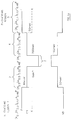
- Figure 1(a) is a schematic band structure of a separate confinement laser structure fabricated in the (Al,Ga,In)P system. It consists of an n-doped (Al 0.7 Ga 0.3 ) 0.52 In 0.48 P cladding region 1, an (Al 0.5 Ga 0.5 ) 0.52 In 0.48 P optical guiding region 2, 4, a GaInP quantum well active region 3 disposed within the (Al 0.5 Ga 0.5 ) 0.52 In 0.48 P optical guiding region, and a p-doped (Al 0.7 Ga 0.3 ) 0.52 In 0.48 P cladding regions.
- a p-type contact layer (not shown in Figure 1(a)) may be provided on the p-type cladding region 5, and an n-type contact layer (also not shown in Figure 1(a)) may be provided on the n-type cladding region 1.
- Optical transitions giving rise to laser action in the quantum well active region 3 of the laser diode originate from electrons in the ⁇ -band in the GaInP quantum well active region.
- ⁇ -band and X-band refer to symmetry points in the Brillouin zone and are standard terms in solid state physics, see for example R. A. Smith “Semiconductors", (Cambridge University Press, 1978).
- ⁇ -minimum and X-minimum refer to the minimum energy level of the ⁇ -band and the X-band, respectively.
- the minimum energy in the conduction band of (Al,Ga,In)P is a function of the aluminium content. There is a crossover from a ⁇ -band minimum to an X-band minimum at an aluminium concentration of about 0.55.
- Figure 1(b) illustrates a similar laser structure to that of Figure 1(a), but the cladding regions 1,5 are formed of AlInP rather than (Al 0.7 Ga 0.3 ) 0.52 In 0.48 P in order to increase the potential barrier confining ⁇ -electrons in the optical guiding region 2.4.
- the active region 3 is shown as containing a single quantum well layer. As is well known, however, the active region 3 may alternatively consist of a plurality of quantum well layers, with each quantum well layer being separated from an adjacent quantum well layer by a barrier layer.
- AlGaAs/GaAs lasers having a lasing wavelength of around 0.85 ⁇ m were initially developed in the 1970s, but early examples of these lasers degraded quickly during use and, as a result, had a low lifetime and were unsuitable for commercial applications. It took a considerable time to overcome the significant degradation problems involved with these lasers.
- One of the main factors in the degradation of AlGaAs/GaAs lasers was crystal defects introduced during the crystal growth and fabrication processes. These defects are known as "dark line" defects, and give rise to a localised region of high non-radiative recombination centres which have high optical absorption.
- MBE molecular beam epitaxy
- phosphide laser structures that are grown by MBE have to be thermally annealed in order to improve their reliability and to decrease the threshold for laser operation. It is presumed that the annealing process removes (or at least moves) some of the non-radiative recombination centres in the material. It is, however, undesirable to carry out an annealing step.
- One common p-type dopant for the p-type cladding region is beryllium, and if a beryllium-doped laser device is annealed beryllium can diffuse from the p-type cladding region into the active region. Such diffusion will degrade the performance of the laser device, and may also lower the yield of the manufacturing process.
- APD anti-phase domain defect
- APDs start to form after about 1 ⁇ m of epitaxial growth, although this depends on the growth parameters such as the growth temperature and the V-III ratio during the growth process.
- APDs usually form in the n-type contact layer (if one is provided) or in the n-type cladding layer 1, and extend right across the semiconductor laser through the active region to the p-type contact layer 6 disposed on the p-type cladding layer 5.
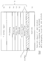
- Figure 2 is a schematic sectional view of an SCH laser, such as the laser of Figure 1(a) or Figure 1(b) fabricated in the (Al,Ga,In)P system.
- APDs 7 run through the laser structure, from the n-type cladding region 1 to the p-type contact region 6.
- EP-A-0 603 780, EP-A-0 421 205, US-A- 5 508 554 and US-A 4 835 166 relate to the growth of a semiconductor layer structure on a substrate that is not lattice-matched to the layer structure.
- the lattice mis-match between the substrate and the layer structure lead to the formation of defects and dislocations, and these documents propose growing a buffer layer at the interface between the substrate and the layer structure to reduce the effects of the lattice mis-match. These documents do not, however, address the problem of the formation and propagation of defects within the layer structure itself.
- Valster et al report that the size of domains caused by ordering can vary by as much as a factor of 50, depending on the growth temperature and the aluminium mole fraction of the layer. They report domain sizes of up to 100s of nm in material grown by MOCVD. T-Y Seong et at (supra) report a smaller domain size for material grown by gas source MBE, of typically 1.5nm. A large number of domain boundaries will cause additional optical loss, and thus decrease the quantum efficiency of the laser device.
- M. Jalonen et al propose that the threshold for laser oscillation of structures grown by MBE can be reduced significantly by annealing the laser structure, in order to remove non-radiative recombination defects. This is not, however, entirely satisfactory since, as noted above, annealing a device that contains beryllium as a dopant can cause diffusion of the beryllium.
- TEM (Transmission Electron-Micrograph) studies of GaInP layers have shown that a large change in the V/III ratio can also suppress the propagation of APDs in GaInP. This is because the domain size depends, among other factors, on the V/III ratio. Thus, changing the V/III ratio during the growth process will change the domain size and will suppress the propagation of APDs. A large change in the temperature during the growth process will also cause a change in the domain size and thus suppress propagation of APDs.
- the disadvantage of changing the V/III ratio or the temperature during the growth process in order to suppress propagation of APDs is that an ordered/disordered interface is set up. This gives rise to a difference in bandgap, and so increases the resistivity of the layer.
- the present invention provides a semiconductor device comprising: a substrate; and a multilayer structure disposed on the substrate , the multilayer structure comprising a first semiconductor layer and a second semiconductor layer disposed on the first semiconductor layer; characterised in that the device further comprises a layer for inhibiting the propagation of defects from the first semiconductor layer into the second semiconductor layer.
- defects such as APDs propagate in the first semiconductor layer, their propagation will be inhibited at the layer for inhibiting the propagation of defects.
- a reduced number of APDs or other defects will reach the second semiconductor layer, and this will reduce the density of absorption defects in the second semiconductor layer, thus improving the characteristics of the layer.
- the second semiconductor layer may be an active layer of the device.
- the first semiconductor layer may be a cladding layer of the device.
- the device may be a separate confinement heterostructure laser device having an optical guiding region disposed on the cladding layer, the active layer being disposed in said optical guiding region.
- the present invention can be applied to a laser device, for example an SCH laser device, to improve the optical characteristics of the active layer of the laser device by inhibiting the propagation of defects such as APDs into the active layer.
- the device may comprise a cladding layer, an optical guiding region and an active layer in this order.
- the layer for inhibiting the propagation of defects may be disposed within the cladding layer.
- the layer for inhibiting the propagation of defects may be disposed at the interface between the cladding layer and the optical guiding region, or it may be disposed within the optical guiding region.
- the device may be an (Al,Ga,In)P device, and the layer for inhibiting the propagation of defects may be a Ga 1-y In y P layer.
- the layer for inhibiting the propagation of defects may be a strained Ga 1-y In y P layer.
- the layer for inhibiting the propagation of defects may be disposed within 1 ⁇ m of the active layer.
- the typical domain size for APDs in a phosphide material is around 1 ⁇ m, so placing the layer for inhibiting the propagation of defects within 1 ⁇ m of the active layer means that APDs cannot re-form in the layers between the active layer and the layer for inhibiting the propagation of defects.
- the bandgap of the layer for inhibiting the propagation of defects maybe substantially equal to the bandgap of a semiconductor layer adjacent to the layer for inhibiting the propagation of defects. This prevents the formation of a significant potential well or potential barrier, thus ensuring that the transport of carriers through the device is unaffected by the provision of the layer for inhibiting the propagation of defects.
- the layer for inhibiting the propagation of defects may be disposed within the first semiconductor layer, and the bandgap of the layer for inhibiting the propagation of defects may be substantially equal to the bandgap of the first semiconductor layer.
- the layer for inhibiting the propagation of defects may be disposed within the optical guiding region, and the bandgap of the layer for inhibiting the propagation of defects may be substantially equal to the bandgap of the optical guiding region.
- the layer for inhibiting the propagation of defects may be disposed at the interface between the cladding layer and the optical guiding region, and the bandgap of the layer for inhibiting the propagation of defects may be substantially equal either to the bandgap of the optical guiding region or to the bandgap of the cladding layer.
- the first semiconductor layer may be an (Al y Ga 1-y ) 0.52 In 0.48 P layer (0.5 ⁇ y ⁇ 1).
- the first semiconductor layer may be an (Al 0.7 Ga 0.3 ) 0.52 In 0.48 P layer and the layer for inhibiting the propagation of defects may be a Ga 0.3 In 0.7 P layer.
- the first semiconductor layer may be an Al 0.52 In 0.48 P layer and the layer for inhibiting the propagation of defects may be a GaP layer.
- the optical guiding region may comprise an (Al y Ga 1-y ) 0.52 In 0.48 P layer (0.3 ⁇ y ⁇ 0.5).
- the optical guiding region may comprise an (Al 0.5 Ga 0.5 ) 0.52 In 0.48 P layer and the layer for inhibiting the propagation of defects may be a Ga 0.38 In 0.62 P layer.
- the bandgaps of the two materials are substantially equal to one another, so that provision of the layer for inhibiting the propagation of defects does not cause a significant potential barrier or potential well.
- the cladding layers and the optical guiding region of an (Al,Ga,In)P laser device are often formed of (Al 0.7 Ga 0.3 ) 0.52 In 0.48 P and (Al 0.5 Ga 0.5 ) 0.52 In 0.48 P respectively, so that the invention allows a layer for inhibiting the propagation of defects to be incorporated into an (Al,Ga,In)P laser device without affecting the transport of carriers through the laser device.
- the device may further comprise a second layer for inhibiting the propagation of defects into the second semiconductor layer.
- the or each layer for inhibiting the propagation of defects may be for inhibiting the propagation of anti-phase domain defects into the second semiconductor layer.
- the characteristic size of an anti-phase domain defect in the or each layer for inhibiting the propagation of defects may be different from the characteristic size of an anti-phase domain defect in the second semiconductor layer. This is a straightforward way of inhibiting the propagation of anti-phase domains.
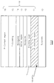
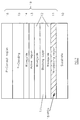
- FIG. 4 shows a laser device according to one embodiment of the invention.
- the laser device has a substrate 10, and a multilayer structure 19 disposed on the substrate 10.
- the multilayer structure 19 comprises an n-type cladding region 11, and an undoped optical guiding region 12, 14 disposed on the n-type cladding region 11.
- An active region 13 is disposed within the optical guiding region 12, 14.
- a p-type cladding region 15 and a p-type contact region 16 are disposed over the optical guiding region 14.
- the active region 3 is shown as containing only a single quantum well layer.
- the invention is not limited to a laser in which the active region contains only one quantum well layer, however, and the invention can be applied to a laser in which the active region 3 consists of a plurality of quantum well layers and barrier layers.
- a blocking layer 17 is provided between the substrate 10 and the active region 13.
- the blocking layer serves to inhibit the propagation of APDs into the active region 13 of the laser device.
- the blocking layer 17 is disposed within the n-type cladding region 11, but the invention is not limited to this particular location for the blocking layer.
- APDs 18 exist in the lower part of the n-type cladding region, but the propagation of APDs into the active layer 13 is inhibited by the blocking layer 17 because the characteristic size of APDs in the blocking layer 17 is significantly different to the characteristic size of APDs within the n-type cladding region 11.
- no APDs (or at least a reduced number of APDs) reach the active region 13. Furthermore, in the embodiment of Figure 4 no APDs, or a reduced number of APDs, reach the optical guiding region 12, 14. In consequence, the laser characteristics of the device are improved.
- the blocking layer 17 need not be located within the n-type cladding region 11, provided it is positioned so that it inhibits the propagation of APDs before they reach the active region 13. It could alternatively be located, for example, at the interface between the n-type cladding region 11 and the optical guiding region 12, as shown in Figure 6. It could alternatively be located within the lower part of the optical guiding region 12 as shown in Figure 7, or at the interface between the lower part of the optical guiding region 12 and the active region 13 as shown in Figure 8.
- the laser structures shown in Figures 6,7 and 8 are generally similar to the laser structure shown in Figure 4. In all the embodiments of Figures 4, 6, 7 and 8, the blocking layer is located between the active region and the substrate, so that it will inhibit the propagation of APDs before they reach the active region 13.
- the blocking region 17 can in principle be disposed at any position below the active region 13. It is however preferable for the blocking layer to be located between the substrate and the optical guiding region 12, in order to inhibit the propagation of APDs into the optical guiding region. If APDs propagate into the optical guiding region 12, or into part of the optical guiding region 12, there will be a deterioration in the laser characteristics, even if the APDs are inhibited from propagating into the active region itself.
- the typical domain size for an APD in a phosphide material is around 1 ⁇ m.
- the blocking layer 17 is preferably disposed within 1 ⁇ m of the active region. This ensures that APDs cannot re-form in the layers above the blocking layer.
- the present invention is not limited to a single blocking layer, but it is possible to provide a laser structure with two or more blocking layers.
- Figure 9 shows an embodiment of the invention in which a laser structure is provided with two blocking layers.
- a first blocking layer 17 is provided within the n-type cladding region 11, and a second blocking layer 17' is provided at the interface between the n-type cladding region 11 and the optical guiding region 12, 14.
- suitable materials for the blocking layer include GaP or Ga 1-y In y P (hereinafter GaInP).
- GaP is an indirect semiconductor with ⁇ - ⁇ and ⁇ - X bandgaps of 2.9eV and 2.3eV respectively, and with a lattice constant of 5.451 ⁇ .
- InP is a direct bandgap material with ⁇ - ⁇ and ⁇ - X bandgaps of 1.4eV and 2.3eV respectively.
- the lattice constant of GaAs is 5.653 ⁇ and, as stated above, GaInP is lattice matched to GaAs when the indium mole fraction, y, is equal to 0.48.
- Bulk GaAs has a lattice constant that is approximately 3.7% greater than that of bulk GaP.
- dislocations would occur at an interface between two semiconductor materials having such a lattice mismatch. This is undesirable in the present case, since these dislocations would degrade the properties of the laser device.
- a laser structure is provided with a blocking layer made of a material whose bulk lattice constant is not lattice matched to the semiconductor layers of the laser structure it is preferable that the thickness of the blocking layer is lower than the critical thickness, to prevent dislocations occuring.
- the blocking layer will be in a strained state and, as result of the strain, will be lattice matched to the semiconductor layers.
- the blocking layer will be in a state of tensile strain since it will have a lower lattice constant than the semiconductor layer.
- the critical thickness at which misfit dislocations will occur is estimated to be 16 ⁇ , see R. People et al, "Applied Physics Letters” Vol. 47 No. 3 pp. 322-324 1985. Where a strained GaP layer is used as the blocking layer, therefore, its thickness is preferably 16 ⁇ or less.
- the blocking layer has a non-zero indium mole fraction.
- the bandgap of GaInP decreases as the indium mole fraction increases, and an advantage of using a tensile strained GaInP layer as the blocking layer is that the bandgaps of the blocking layer can be tuned to the bandgaps of the various quarternary alloys used in the laser structure, by appropriately adjusting the indium mole fraction of the blocking layer.
- a tensile strained layer of Ga 0.3 In 0.7 P has ⁇ - ⁇ and ⁇ - X bandgaps of 2.450eV and 2.3eV respectively, and these bandgaps are the same as those of (Al 0.7 Ga 0.3 ) 0.52 In 0.48 P which is commonly used as a material for the cladding layers of a laser device.
- the critical thickness when a strained Ga 0.3 In 0.7 P layer is grown on an (Al 0.7 Ga 0.3 ) 0.52 In 0.48 P layer is 33 ⁇ , so it is preferable for the thickness of the blocking layer to be less than this.
- Another useful material for the blocking layer is a tensile strained layer of Ga 0.38 In 0.62 P.
- the ⁇ - ⁇ and ⁇ - X bandgaps of this material are 2.3eV, which are the same as in (Al 0.5 Ga 0.5 ) 0.52 In 0.48 P, which is used to form the optical guiding layers of the laser devices shown in Figures 1(a) and 1(b). Since the bandgaps of (Al 0.5 Ga 0.5 ) 0.52 In 0.48 P and Ga 0.38 In 0.62 P are approximately equal, a Ga 0.38 In 0.62 P blocking layer can be provided within an (Al 0.5 Ga 0.5 ) 0.52 In 0.48 P optical guiding layer without introducing a significant potential well or potential barrier.
- the critical thickness for Ga 0.38 In 0.62 P layer is around 60 ⁇ .
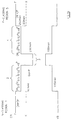
- Figure 5 is a partial schematic bandgap diagram of the laser device of Figure 4.
- Figure 5 shows the bandgaps for the n-cladding region 11, the blocking layer 17 and part of the optical guiding region 12.
- the n-type cladding region 11 is formed of (Al 0.7 Ga 0.3 ) 0.52 In 0.48 P
- the optical guiding region is formed of (Al 0.5 Ga 0.5 ) 0.52 In 0.48 P.
- the blocking layer 17 is disposed within the n-type cladding region 11, and is formed of a strained layer of Ga 0.3 In 0.7 P.
- the ⁇ - ⁇ and ⁇ - X bandgaps of the blocking layer 17 are similar to those of the cladding region in which the blocking layer is provided, so that no potential barriers or potential well is formed.
- the thickness of the blocking layer 17 should be less than 33 ⁇ , which is the critical thickness of a layer of Ga 0.3 In 0.7 P layer mismatched to GaAs.
- the blocking layer were provided in the optical guiding region 12 rather than in the n-type cladding region 11, it would be preferable for the blocking layer to be formed of Ga 0.38 In 0.62 P. This material is bandgap matched to an (Al 0.5 Ga 0.5 ) 0.52 In 0.48 P optical guiding region.
- the bandgaps of the blocking layer can be matched either of the layers.
- the present invention is not limited to this system. It can be applied to any materials system which shows an ordering effect such that the propagation of defects such as APDs through a semiconductor structure cause significant degradation of the device properties.
- the blocking layer of Figure 5 has bandgaps that are similar to the bandgaps of the layer in which the blocking layer is placed, this is not an essential feature of the invention. It is, however, a preferred feature, since any mis-match in the bandgap will cause either a potential barrier or a potential well, and this will disrupt transport of carriers into the active region of the device.
- the present invention is of particular advantage when applied to semiconductor laser devices, since these are very sensitive to defects.
- the present invention is not, however, limited to laser devices but can be applied to other semiconductor devices such as, for example, light-emitting diodes.
Landscapes
- Physics & Mathematics (AREA)
- Optics & Photonics (AREA)
- Condensed Matter Physics & Semiconductors (AREA)
- General Physics & Mathematics (AREA)
- Electromagnetism (AREA)
- Chemical & Material Sciences (AREA)
- Engineering & Computer Science (AREA)
- Nanotechnology (AREA)
- Life Sciences & Earth Sciences (AREA)
- Biophysics (AREA)
- Crystallography & Structural Chemistry (AREA)
- Semiconductor Lasers (AREA)
Applications Claiming Priority (2)
| Application Number | Priority Date | Filing Date | Title |
|---|---|---|---|
| GB9915672A GB2351841A (en) | 1999-07-06 | 1999-07-06 | A semiconductor laser device |
| GB9915672 | 1999-07-06 |
Publications (2)
| Publication Number | Publication Date |
|---|---|
| EP1067594A2 true EP1067594A2 (de) | 2001-01-10 |
| EP1067594A3 EP1067594A3 (de) | 2002-07-10 |
Family
ID=10856638
Family Applications (1)
| Application Number | Title | Priority Date | Filing Date |
|---|---|---|---|
| EP00305647A Withdrawn EP1067594A3 (de) | 1999-07-06 | 2000-07-05 | Halbleitervorrichtung |
Country Status (6)
| Country | Link |
|---|---|
| US (1) | US6631150B1 (de) |
| EP (1) | EP1067594A3 (de) |
| JP (1) | JP2001053389A (de) |
| KR (1) | KR100378504B1 (de) |
| GB (1) | GB2351841A (de) |
| TW (1) | TW546849B (de) |
Cited By (2)
| Publication number | Priority date | Publication date | Assignee | Title |
|---|---|---|---|---|
| EP2408027A4 (de) * | 2009-03-10 | 2015-05-27 | Showa Denko Kk | Lichtemittierende diode, lampe mit einer lichtemittierenden diode und beleuchtungsvorrichtung |
| WO2021110585A1 (de) * | 2019-12-05 | 2021-06-10 | Osram Opto Semiconductors Gmbh | Strahlungsemittierender halbleiterchip |
Families Citing this family (18)
| Publication number | Priority date | Publication date | Assignee | Title |
|---|---|---|---|---|
| US7369043B2 (en) * | 2005-05-11 | 2008-05-06 | Ford Global Technologies, Llc | Method and apparatus for automatically identifying the location of pressure sensors in a tire pressure monitoring system |
| US20100203730A1 (en) * | 2009-02-09 | 2010-08-12 | Emcore Solar Power, Inc. | Epitaxial Lift Off in Inverted Metamorphic Multijunction Solar Cells |
| JP2010067903A (ja) * | 2008-09-12 | 2010-03-25 | Toshiba Corp | 発光素子 |
| US8778199B2 (en) | 2009-02-09 | 2014-07-15 | Emoore Solar Power, Inc. | Epitaxial lift off in inverted metamorphic multijunction solar cells |
| US8975615B2 (en) | 2010-11-09 | 2015-03-10 | Soraa Laser Diode, Inc. | Method of fabricating optical devices using laser treatment of contact regions of gallium and nitrogen containing material |
| US9048170B2 (en) * | 2010-11-09 | 2015-06-02 | Soraa Laser Diode, Inc. | Method of fabricating optical devices using laser treatment |
| US9025635B2 (en) | 2011-01-24 | 2015-05-05 | Soraa Laser Diode, Inc. | Laser package having multiple emitters configured on a support member |
| US8971370B1 (en) | 2011-10-13 | 2015-03-03 | Soraa Laser Diode, Inc. | Laser devices using a semipolar plane |
| US10559939B1 (en) | 2012-04-05 | 2020-02-11 | Soraa Laser Diode, Inc. | Facet on a gallium and nitrogen containing laser diode |
| CN104167662A (zh) * | 2014-06-26 | 2014-11-26 | 南京青辰光电科技有限公司 | 一种量子阱结构的宽谱激光器 |
| US11437774B2 (en) | 2015-08-19 | 2022-09-06 | Kyocera Sld Laser, Inc. | High-luminous flux laser-based white light source |
| US11421843B2 (en) | 2018-12-21 | 2022-08-23 | Kyocera Sld Laser, Inc. | Fiber-delivered laser-induced dynamic light system |
| US11239637B2 (en) | 2018-12-21 | 2022-02-01 | Kyocera Sld Laser, Inc. | Fiber delivered laser induced white light system |
| US12000552B2 (en) | 2019-01-18 | 2024-06-04 | Kyocera Sld Laser, Inc. | Laser-based fiber-coupled white light system for a vehicle |
| US11884202B2 (en) | 2019-01-18 | 2024-01-30 | Kyocera Sld Laser, Inc. | Laser-based fiber-coupled white light system |
| US12152742B2 (en) | 2019-01-18 | 2024-11-26 | Kyocera Sld Laser, Inc. | Laser-based light guide-coupled wide-spectrum light system |
| US11670913B2 (en) * | 2020-06-26 | 2023-06-06 | Lumentum Operations Llc | Semiconductor layer structure with a thin blocking layer |
| CN112636180B (zh) * | 2021-03-10 | 2021-06-01 | 陕西源杰半导体科技股份有限公司 | 激光器芯片及制备方法 |
Family Cites Families (13)
| Publication number | Priority date | Publication date | Assignee | Title |
|---|---|---|---|---|
| US4835116A (en) * | 1987-11-13 | 1989-05-30 | Kopin Corporation | Annealing method for III-V deposition |
| US5048036A (en) * | 1989-09-18 | 1991-09-10 | Spectra Diode Laboratories, Inc. | Heterostructure laser with lattice mismatch |
| US5021360A (en) * | 1989-09-25 | 1991-06-04 | Gte Laboratories Incorporated | Method of farbicating highly lattice mismatched quantum well structures |
| JP2817995B2 (ja) | 1990-03-15 | 1998-10-30 | 富士通株式会社 | ▲iii▼―▲v▼族化合物半導体ヘテロ構造基板および▲iii▼―▲v▼族化合物ヘテロ構造半導体装置 |
| JPH05291686A (ja) | 1992-04-14 | 1993-11-05 | Matsushita Electric Ind Co Ltd | 半導体レーザ |
| JP3097939B2 (ja) | 1992-10-26 | 2000-10-10 | 日本電信電話株式会社 | 面発光半導体レーザ |
| EP0603780B1 (de) * | 1992-12-21 | 1998-04-29 | Nippon Steel Corporation | Verfahren zum Wachstum von Verbundhalbleitern auf einer Siliziumscheibe |
| JPH0766366A (ja) * | 1993-08-26 | 1995-03-10 | Hitachi Ltd | 半導体積層構造体およびそれを用いた半導体装置 |
| US5665977A (en) | 1994-02-16 | 1997-09-09 | Sony Corporation | Semiconductor light emitting device with defect decomposing and blocking layers |
| JP3785660B2 (ja) | 1995-10-17 | 2006-06-14 | ソニー株式会社 | 半導体発光素子 |
| JPH1084161A (ja) * | 1996-09-06 | 1998-03-31 | Sumitomo Electric Ind Ltd | 半導体レーザ及びその製造方法 |
| US5838705A (en) | 1996-11-04 | 1998-11-17 | Motorola, Inc. | Light emitting device having a defect inhibition layer |
| JPH10290046A (ja) | 1997-04-16 | 1998-10-27 | Sony Corp | AlGaInP系半導体発光素子ならびに光ディスク記録および/または再生装置 |
-
1999
- 1999-07-06 GB GB9915672A patent/GB2351841A/en not_active Withdrawn
-
2000
- 2000-07-05 US US09/610,019 patent/US6631150B1/en not_active Expired - Fee Related
- 2000-07-05 EP EP00305647A patent/EP1067594A3/de not_active Withdrawn
- 2000-07-05 JP JP2000204086A patent/JP2001053389A/ja not_active Withdrawn
- 2000-07-06 TW TW089113399A patent/TW546849B/zh not_active IP Right Cessation
- 2000-07-06 KR KR10-2000-0038522A patent/KR100378504B1/ko not_active Expired - Fee Related
Cited By (2)
| Publication number | Priority date | Publication date | Assignee | Title |
|---|---|---|---|---|
| EP2408027A4 (de) * | 2009-03-10 | 2015-05-27 | Showa Denko Kk | Lichtemittierende diode, lampe mit einer lichtemittierenden diode und beleuchtungsvorrichtung |
| WO2021110585A1 (de) * | 2019-12-05 | 2021-06-10 | Osram Opto Semiconductors Gmbh | Strahlungsemittierender halbleiterchip |
Also Published As
| Publication number | Publication date |
|---|---|
| JP2001053389A (ja) | 2001-02-23 |
| TW546849B (en) | 2003-08-11 |
| KR20010029894A (ko) | 2001-04-16 |
| EP1067594A3 (de) | 2002-07-10 |
| US6631150B1 (en) | 2003-10-07 |
| GB2351841A (en) | 2001-01-10 |
| KR100378504B1 (ko) | 2003-03-31 |
| GB9915672D0 (en) | 1999-09-01 |
Similar Documents
| Publication | Publication Date | Title |
|---|---|---|
| US6631150B1 (en) | Semiconductor device | |
| EP1182756B1 (de) | Halbleiterlaservorrichtung mit niedrigerem Schwellstrom | |
| US7622745B2 (en) | Epitaxial wafer for a semiconductor light emitting device, method for fabricating the same and semiconductor light emitting device | |
| JPH1065271A (ja) | 窒化ガリウム系半導体光発光素子 | |
| JPH11274635A (ja) | 半導体発光装置 | |
| US6486491B1 (en) | Semiconductor device | |
| US5003548A (en) | High power (1,4 W)AlGaInP graded-index separate confinement heterostructure visible (λ-658 nm) laser | |
| US5406574A (en) | Semiconductor laser device | |
| EP1147584B1 (de) | Optische halbleitervorrichtung | |
| US5561080A (en) | Semiconductor laser and method for fabricating the same | |
| EP0952645B1 (de) | Halbleiterlaservorrichtung | |
| JP2956623B2 (ja) | 自励発振型半導体レーザ素子 | |
| JP3889910B2 (ja) | 半導体発光装置およびその製造方法 | |
| EP0544357B1 (de) | Strahlung emittierende Halbleiterdiode | |
| JPH1022586A (ja) | 半導体発光素子 | |
| JP2007194561A (ja) | 面発光レーザ | |
| EP0784361B1 (de) | Halbleiterlaservorrichtung und Herstellungsverfahren | |
| JP2914330B2 (ja) | 自励発振型半導体レーザ素子の成長方法 | |
| Watanabe et al. | High-temperature operation (70/spl deg/C, 50 mW) of 660-nm-band InGaAlP Zn-diffused window lasers fabricated using highly Zn-doped GaAs layers | |
| JP3279308B2 (ja) | 窒化物半導体発光素子 | |
| JP2005136274A (ja) | 半導体レーザダイオードの製造方法 | |
| JPH08274409A (ja) | 半導体発光装置 |
Legal Events
| Date | Code | Title | Description |
|---|---|---|---|
| PUAI | Public reference made under article 153(3) epc to a published international application that has entered the european phase |
Free format text: ORIGINAL CODE: 0009012 |
|
| AK | Designated contracting states |
Kind code of ref document: A2 Designated state(s): AT BE CH CY DE DK ES FI FR GB GR IE IT LI LU MC NL PT SE |
|
| AX | Request for extension of the european patent |
Free format text: AL;LT;LV;MK;RO;SI |
|
| PUAL | Search report despatched |
Free format text: ORIGINAL CODE: 0009013 |
|
| AK | Designated contracting states |
Kind code of ref document: A3 Designated state(s): AT BE CH CY DE DK ES FI FR GB GR IE IT LI LU MC NL PT SE |
|
| AX | Request for extension of the european patent |
Free format text: AL;LT;LV;MK;RO;SI |
|
| 17P | Request for examination filed |
Effective date: 20021029 |
|
| AKX | Designation fees paid |
Designated state(s): DE FR GB |
|
| 17Q | First examination report despatched |
Effective date: 20030508 |
|
| STAA | Information on the status of an ep patent application or granted ep patent |
Free format text: STATUS: THE APPLICATION IS DEEMED TO BE WITHDRAWN |
|
| 18D | Application deemed to be withdrawn |
Effective date: 20030919 |