EP1067620A2 - Dielektrisches Filter, dielektrischer Duplexer und Kommunikationsgerät damit - Google Patents
Dielektrisches Filter, dielektrischer Duplexer und Kommunikationsgerät damit Download PDFInfo
- Publication number
- EP1067620A2 EP1067620A2 EP00113283A EP00113283A EP1067620A2 EP 1067620 A2 EP1067620 A2 EP 1067620A2 EP 00113283 A EP00113283 A EP 00113283A EP 00113283 A EP00113283 A EP 00113283A EP 1067620 A2 EP1067620 A2 EP 1067620A2
- Authority
- EP
- European Patent Office
- Prior art keywords
- dielectric
- holes
- conductor
- dielectric block
- mode
- Prior art date
- Legal status (The legal status is an assumption and is not a legal conclusion. Google has not performed a legal analysis and makes no representation as to the accuracy of the status listed.)
- Granted
Links
- 239000004020 conductor Substances 0.000 claims description 45
- 230000005284 excitation Effects 0.000 description 23
- 230000008878 coupling Effects 0.000 description 9
- 238000010168 coupling process Methods 0.000 description 9
- 238000005859 coupling reaction Methods 0.000 description 9
- 230000004323 axial length Effects 0.000 description 6
- 230000005540 biological transmission Effects 0.000 description 3
- UUDAMDVQRQNNHZ-UHFFFAOYSA-N (S)-AMPA Chemical compound CC=1ONC(=O)C=1CC(N)C(O)=O UUDAMDVQRQNNHZ-UHFFFAOYSA-N 0.000 description 2
- 230000007423 decrease Effects 0.000 description 1
- 238000010586 diagram Methods 0.000 description 1
- 238000003199 nucleic acid amplification method Methods 0.000 description 1
- 230000008054 signal transmission Effects 0.000 description 1
Images


Classifications
-
- H—ELECTRICITY
- H01—ELECTRIC ELEMENTS
- H01P—WAVEGUIDES; RESONATORS, LINES, OR OTHER DEVICES OF THE WAVEGUIDE TYPE
- H01P1/00—Auxiliary devices
- H01P1/20—Frequency-selective devices, e.g. filters
- H01P1/201—Filters for transverse electromagnetic waves
- H01P1/205—Comb or interdigital filters; Cascaded coaxial cavities
- H01P1/2056—Comb filters or interdigital filters with metallised resonator holes in a dielectric block
-
- H—ELECTRICITY
- H01—ELECTRIC ELEMENTS
- H01P—WAVEGUIDES; RESONATORS, LINES, OR OTHER DEVICES OF THE WAVEGUIDE TYPE
- H01P1/00—Auxiliary devices
- H01P1/20—Frequency-selective devices, e.g. filters
- H01P1/213—Frequency-selective devices, e.g. filters combining or separating two or more different frequencies
- H01P1/2136—Frequency-selective devices, e.g. filters combining or separating two or more different frequencies using comb or interdigital filters; using cascaded coaxial cavities
-
- H—ELECTRICITY
- H01—ELECTRIC ELEMENTS
- H01P—WAVEGUIDES; RESONATORS, LINES, OR OTHER DEVICES OF THE WAVEGUIDE TYPE
- H01P1/00—Auxiliary devices
- H01P1/20—Frequency-selective devices, e.g. filters
- H01P1/207—Hollow waveguide filters
- H01P1/208—Cascaded cavities; Cascaded resonators inside a hollow waveguide structure
- H01P1/2084—Cascaded cavities; Cascaded resonators inside a hollow waveguide structure with dielectric resonators
-
- H—ELECTRICITY
- H01—ELECTRIC ELEMENTS
- H01P—WAVEGUIDES; RESONATORS, LINES, OR OTHER DEVICES OF THE WAVEGUIDE TYPE
- H01P7/00—Resonators of the waveguide type
- H01P7/10—Dielectric resonators
Definitions
- the present invention relates to dielectric filters and dielectric duplexers used in microwave bands and millimeter-wave bands, and the invention also relates to communication apparatuses using the same.
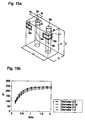
- Fig. 15A shows a perspective view of a conventional dielectric filter obtained by forming conductor films on a dielectric block and therein.
- reference numeral 1 denotes a substantially rectangular-parallelepiped dielectric block, in which inner-conductor-formed holes 2a and 2b having inner conductors 3a and 3b formed on the inner surfaces thereof are formed.
- an outer conductor 4 is each formed on external surfaces of the dielectric block 1.
- a non-inner-conductor-formed position g is disposed on the inner surface of each of the inner-conductor-formed holes 2a and 2b.
- input/output electrodes 5a and 5b are formed in such a manner that the electrodes 5a and 5b are isolated from the outer conductors 4.
- TEM-mode dielectric resonators are formed by using the dielectric block, the inner conductors, and the outer conductors.
- a comb-line coupling between the dielectric resonators is performed by stray capacitances generated at the non-inner-conductor-formed portions g so as to form a dielectric filter constituted of the two-stage resonator as an overall structure.
- the outline dimensions of the dielectric block, the dimensions of the inner-conductor-formed holes, and the positions of the inner-conductor-formed holes disposed inside the dielectric block are determined.
- the unloaded Q of the resonator increases depending on both the thickness tb between the inner-conductor-formed hole and a widthwise line of the dielectric block and the thickness ta between the inner-conductor-formed hole and a lengthwise line of thereof.
- Fig. 15B shows the relationship between the ratio of the thickness ta to the thickness tb as the aforementioned two distances and the unloaded Q of the resonator obtained when the length of a widthwise line C of a plane perpendicular to an axis of each of the inner-conductor-formed holes of the dielectric block is set to be 2.0 mm, the length of a lengthwise line H thereof is set to be 4.0 mm, and the axial length D of the inner-conductor-formed hole is set to be 4.0 mm.
- the larger the ratio of tb/ta the higher the unloaded Q of the resonator.
- the thickness tb is set to be substantially equal to the thickness ta.
- a spurious mode becomes problematic when the spurious mode occurs in a band requiring attenuation, for example, a band of a higher-order frequency than the central frequency of a pass band of the dielectric filter.
- a conventional dielectric filter for example, as shown in Japanese Unexamined Patent Application Publication No. 8-51301, a part of an outer conductor formed on a dielectric-block end face closer to a non-conductor-formed portion is cut away to adjust the resonance frequency of a spurious mode, and, then, the spurious-mode frequency is isolated from a TEM-mode resonance frequency so that influence of the spurious mode can be avoided.
- the overall structure of the dielectric filter is complicated, such an arrangement causes a problem of an increase in production cost.
- preferred embodiments of the present invention provide a dielectric filter and a dielectric duplexer each having a simple structure, in which control can be given in such a manner that no TE-mode spurious response occurs in a band requiring attenuation. Further, the preferred embodiments of the present invention provide a communication apparatus using one of the dielectric filter and the dielectric duplexer.
- One preferred embodiment of the present invention provides a dielectric filter and a dielectric duplexer each including a substantially rectangular-parallelepiped dielectric block, a plurality of holes formed inside the dielectric block, the holes aligned in parallel with each other along a lengthwise line of the dielectric block, inner conductors formed on the inner surfaces of the plurality of the holes and outer conductors formed on external surfaces of the dielectric block.
- the distance between the central axis of an outermost hole of the aligned holes and a widthwise line of the dielectric block is set to be two times or more than the distance between the central axis of the outermost hole and a lengthwise line thereof.
- the dielectric block since designing of the dielectric block permits the frequency of a spurious mode such as a TE 101 mode to be shifted to the lower-frequency side, the influence of the spurious mode can be prevented. As a result, since it is unnecessary to cut away a part of the outer conductor formed on the end face of the dielectric block, production cost can be reduced.
- Another preferred embodiment of the present invention provides a communication apparatus including one of the dielectric filter and the dielectric duplexer, which may be used in a high-frequency circuit section relating to signal transmission/reception in the communication apparatus.
- the influence of a spurious mode such as a TE 101 mode can be prevented in the dielectric filter and the dielectric duplexer. As a result, limited frequency bands can be effectively used.
- Fig. 1A shows a perspective view of a dielectric filter
- Fig. 1B shows a partial plan view of an open face of an inner-conductor-formed hole.
- inner-conductor-formed holes 2a and 2b having inner conductors 3a and 3b formed on the inner surfaces thereof are disposed, and on each of the external six surfaces of the rectangular-parallelepiped dielectric block 1, an outer conductor 4 is disposed.
- non-inner-conductor-formed portions g are disposed on the inner surfaces of the inner-conductor-formed portions g are disposed.
- input/output electrodes 5a and 5b are disposed in such a manner that the electrodes 5a and 5b are isolated from the outer conductors 4.
- the arrangement made by using the dielectric block 1, the inner conductors 3a and 3b, and the outer conductors 4 forms two TEM-mode dielectric resonators, and stray capacitances occurring at the non-inner-conductor-formed portions g permit comb-line coupling between the two resonators to be performed.
- a dielectric filter comprised of the two-stage resonator is formed.
- a lengthwise line of the dielectric block 1 is indicated by the symbol H and a widthwise line thereof is indicated by the symbol C, with the axial length D thereof, the distance B from the center of the inner-conductor-formed hole 2a to the widthwise line C of the dielectric block, the distance A from the center of the inner-conductor-formed hole 2a to the lengthwise line H of the dielectric block, and the width d of the inner diameter of the inner-conductor-formed hole 2a.
- the dimension H also changes.
- Fig. 2 shows the relationship between the amount of changes in the dimension B and the amount of changes in the TE 101 -mode resonant frequency.
- the dimension H is 4.0 mm
- the dimension C is 2.0 mm
- the dimension D is 4.0 mm
- the distance A is 1.0 mm
- the inner-diameter width d is 1.0 mm.
- Fig. 3 shows the pass characteristics of the dielectric filter.
- the symbol f 0 represents the TEM-mode resonance frequency obtained by the inner-conductor-formed holes, the dielectric block, and the outer conductors shown in Fig. 1A.
- the TEM-mode resonance frequency is a central frequency and a specified bandwidth is set as a pass band.
- an attenuation pole appearing on the high-frequency side of the pass band is equivalent to an attenuation pole produced by the comb-line coupling of the above two resonators.
- the symbol f s represents the above TE 101 -mode resonance frequency.
- the resonance frequency f s is shifted to a direction indicated by the symbol f s' .
- the band in the vicinity of a harmonic 2f 0 of the central frequency f 0 in the pass band is set as a band requiring attenuation, responses of the harmonic 2f 0 in the frequency band can be suppressed by shifting the TE 101 -mode resonance frequency to the lower-frequency side.
- Fig. 4 shows the relationship between the ratio of the dimension B to the dimension A and the characteristic impedance Zx of a resonator. Regardless of the inner-diameter width d of an inner-conductor-formed hole, when the ratio of B/A is 2 or larger, the characteristic impedance Zx of the resonator hardly changes. As a result, it is found that increases in the dimension B give no influence on the characteristic impedance. Therefore, in the present invention, since the ratio of B/A is 2 or larger, without giving any influence on the characteristic impedance of the resonator, the TE 101 -mode resonance frequency can be appropriately determined as required.
- Fig. 5A shows a perspective view of the dielectric filter
- Fig. 5B shows a partial plan view of the open face of an inner-conductor-formed hole.
- inner-conductor-formed holes 2a and 2b having inner conductors 3a and 3b formed on the inner surfaces thereof and excitation holes 6a and 6b having conductors formed on the inner surfaces thereof are formed in parallel with each other.
- An outer conductor 4 is each formed on the external six surfaces of the dielectric block 1, and non-inner-conductor-formed portions g are formed on the inner surfaces of the inner-conductor-formed holes 2a and 2b.
- input/output electrodes 5a and 5b are formed such that the electrodes 5a and 5b are isolated from the outer conductors 4.
- One end of each of the excitation holes 6a and 6b is connected to the input/output electrodes 5a and 5b, and the other end of each of the excitation holes 6a and 6b is connected to the outer conductor 4 in the open faces thereof.
- each of the excitation holes is used to obtain an external coupling as an interdigital coupling
- the magnitude of the external coupling can be controlled by the distance between each of the excitation holes and each of the resonators regardless of the length of the dimension B. As a result, freedom in the magnitude of the dimension B is increased.
- Fig. 6 shows the relationship between the amount of changes in the dimension B and the TE 101 -mode resonance frequency of obtained when the dimension B is changed while the distance between the two inner-conductor-formed holes 2a and 2b and the distance between the excitation holes 6a and 6b and the inner-conductor-formed holes 2a and 2b shown in Figs. 5A and 5B remain fixed.
- an arrangement is made such that the dimension H is 5.0 mm, the width C is 2.0 mm, the height D is 4.0 mm, the inner-diameter width d of the inner-conductor-formed hole 2a is 1.0 mm, the distance A is 0.75 mm, and the inner-diameter width d of the excitation hole 6a is 0.5 mm.
- the distance B is 0.75 mm, this shows that ⁇ B is equal to zero.
- the characteristic impedance of the excitation hole hardly changes when the ratio of B/A is 2 or larger, regardless of the inner-diameter width d of the excitation hole, and increases in the dimension B thereby give no influence on the characteristic impedance thereof.
- the TE 101 -mode resonance frequency can be appropriately determined as required.
- Fig. 7 is a perspective view of the appearance of a dielectric filter according to a third embodiment of the present invention.
- a substantially rectangular-parallelepiped dielectric block 1 three inner-conductor-formed holes 2a, 2b, and 2c are disposed, and on the external surfaces of the dielectric block 1, an outer conductor 4 is each formed.
- an open face of each of inner-conductor-formed holes 2a to 2c of the dielectric block 1 is used as an open-circuited end.
- the inner-conductor-formed holes 2a to 2c are stepped holes in which the widths of the inner diameters of the holes on the open-circuited-end sides differ from those on the short-circuited-end sides.
- the value of the TE 101 -mode resonance frequency is close to approximately one half that of the case of the dielectric block having both ends short-circuited.
- Fig. 8 is a perspective view of the appearance of a dielectric filter according to a fourth embodiment.
- a three-stage resonator is formed by using the resonator of the dielectric filter shown in Fig. 1A, and stepped holes are used as inner-conductor-formed holes.
- the distance B between the center of each of the outermost inner-conductor-formed holes 2a and 2c and each of the widthwise lines of a dielectric block is set to be two times or greater than the distance A between the center of each of the outermost holes 2a and 2c and each of the lengthwise lines of the dielectric block.
- Fig. 9 is a perspective view of the appearance of a dielectric filter according to a fifth embodiment of the present invention.
- an open face of each of inner-conductor-formed holes 2a to 2c of a dielectric block 1 is used as an open-circuited face, on which coupling electrodes 7a to 7c extending from inner conductors 3a to 3c are formed. This arrangement permits capacitive couplings between adjacent resonators to be performed.
- the distance B between the center of each of the outermost inner-conductor-formed holes 2a and 2c and each of the widthwise lines of a dielectric block is set to be two times or greater than the distance A between the center of each of the holes 2a and 2c and each of the lengthwise lines thereof.
- Fig. 10 is a perspective view of the appearance of a dielectric filter according to a sixth embodiment of the present invention.
- stepped holes are used as the inner-conductor-formed holes 2a and 2b shown in Figs. 5A and 5B.
- the inner-conductor-formed holes 2a and 2b are stepped holes, an axial length necessary to obtain a specified resonance frequency can be changed, although an axial length in the case of straight holes cannot be changed.
- the resonance frequency with respect to a coaxial length decreases so that the axial length to obtain a specified resonance frequency can be shortened.
- the TE 101 -mode resonance frequency is shifted to the higher-frequency side.
- the TE 101 -mode resonance frequency can be shifted to a frequency side lower than the second-order harmonic 2f 0 of the central frequency f 0 of a pass band.
- the resonance frequency with respect to the coaxial length rises, and the axial length to obtain a specified resonance frequency increases.
- the TE 101 -mode resonance frequency can be shifted to the lower frequency side.
- input/output electrodes 5a and 5b are formed in such a manner that the electrodes 5a and 5b are isolated from the outer conductors 4.
- a capacitance is generated between the electrodes 5a and 5b and the vicinities of the open-circuited ends of the inner conductors formed on the inner surfaces of the inner-conductor-formed holes 2a and 2f.
- the three-stage resonator comprised of the inner-conductor-formed holes 2a to 2c permits band-pass characteristics to be generated between the input/output electrode 5a and the input/output electrode 5c.
- the input/output electrode 5a serves as a transmission signal input terminal
- the input/output electrode 5c serves as an antenna terminal.
- the three-stage resonator comprised of the inner-conductor-formed holes 2d to 2f permits band-pass characteristics to be generated between the input/output electrode 5c and the input/output electrode 5b.
- the input/output electrode 5c serves as an antenna terminal
- the input/output electrode 5b serves as a reception signal output terminal.
- the distance B from the center of each of the outermost inner-conductor-formed holes 2a and 2f to each of the widthwise lines of the dielectric block is two times or greater than the distance A from the center of each of the holes 2a and 2f to each of the lengthwise lines thereof.
- an outer conductor 4 is formed on each of the external six surfaces of a dielectric block.
- the outer conductor 4 is connected to one end of each of inner conductors formed on the inner surfaces of inner-conductor-formed holes. The other end of thereof is open-circuited at a non-inner-conductor-formed portion g.
- the other structural parts are the same as those shown in Fig. 11.
- inner-conductor-formed holes 2a to 2d and excitation holes 6a to 6c having inner conductors formed on the inner surfaces thereof are disposed.
- input/output electrodes 5a to 5c isolated from an outer conductor 4 are formed, and one end of each of the excitation holes 6a to 6c is connected to the input/output electrodes 5a to 5c, respectively.
- the excitation holes 6a and 6c are interdigitally coupled with resonators comprised of the inner-conductor-formed holes 2a and 2b, respectively, and the excitation holes 6c and 6b are interdigitally coupled with resonators comprised of the inner-conductor-formed holes 2c and 2d, respectively.
- the two-stage resonator comprised of the inner-conductor-formed holes 2a and 2b permits pass-band characteristics to be generated between the input/output electrodes 5a to 5c, and the input/output electrode 5a serves as a transmission signal input terminal, and the input/output electrode 5c serves as an antenna terminal.
- the two-stage resonator comprised of the inner-conductor-formed holes 2c and 2d permits pass-band characteristics to be generated between the input/output electrodes 5c to 5b, and the input/output electrode 5c serves as an antenna terminal, and the input/output electrode 5b serves as a reception signal input terminal.
- the distance B from the center of each of the outermost excitation holes 6a and 6b to each of the widthwise lines of the dielectric block is two times or greater than the distance A from the center of each of the holes 6a and 6b to each of the lengthwise lines thereof.
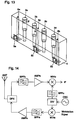
- reference character ANT denotes a transmission/reception antenna
- reference character DPX denotes a duplexer
- reference characters BPFa, BPFb, and BPFc denote band pass filters
- reference characters AMPa and AMPb denote amplifying circuits
- reference characters MIXa and MIXb denote mixers
- reference character OSC denotes an oscillator
- reference character DIV denotes a divider.
- the MIXa modulates a frequency signal output from the DIV by using a modulation signal.
- the BPFa permits only the signals of a transmission-frequency band to pass, and the AMPa performs the power-amplification of the passed signals to transmit from the ANT via the DPX.
- the BPFb permits only the signals of a reception frequency band to pass, and the AMPb amplifies the passed signals.
- the MIXb performs mixing of the frequency signals output from the BPFc and received signals to output intermediate frequency signals IF.
- the aforementioned dielectric duplexer can be used.
- the aforementioned dielectric filter can be used as one of the band-pass filters BPFa, BPFb, and BPFc. In this way, a communication apparatus using one of the dielectric duplexer and the dielectric filter causing no unnecessary spurious-mode responses is obtainable.
Landscapes
- Physics & Mathematics (AREA)
- Electromagnetism (AREA)
- Control Of Motors That Do Not Use Commutators (AREA)
Applications Claiming Priority (2)
| Application Number | Priority Date | Filing Date | Title |
|---|---|---|---|
| JP11179675A JP2001007605A (ja) | 1999-06-25 | 1999-06-25 | 誘電体フィルタ、誘電体デュプレクサおよび通信装置 |
| JP17967599 | 1999-06-25 |
Publications (3)
| Publication Number | Publication Date |
|---|---|
| EP1067620A2 true EP1067620A2 (de) | 2001-01-10 |
| EP1067620A3 EP1067620A3 (de) | 2002-04-24 |
| EP1067620B1 EP1067620B1 (de) | 2008-05-28 |
Family
ID=16069919
Family Applications (1)
| Application Number | Title | Priority Date | Filing Date |
|---|---|---|---|
| EP00113283A Expired - Lifetime EP1067620B1 (de) | 1999-06-25 | 2000-06-21 | Dielektrisches Filter, dielektrischer Duplexer und Kommunikationsgerät damit |
Country Status (6)
| Country | Link |
|---|---|
| US (1) | US6340921B1 (de) |
| EP (1) | EP1067620B1 (de) |
| JP (1) | JP2001007605A (de) |
| KR (1) | KR100343320B1 (de) |
| CN (1) | CN1147961C (de) |
| DE (1) | DE60039007D1 (de) |
Cited By (4)
| Publication number | Priority date | Publication date | Assignee | Title |
|---|---|---|---|---|
| EP1227535A1 (de) * | 2001-01-22 | 2002-07-31 | Murata Manufacturing Co., Ltd. | Dielektrischer Duplexer und Kommunikationsgerät |
| EP1249887A3 (de) * | 2001-04-10 | 2003-07-30 | Murata Manufacturing Co., Ltd. | Dielektrischer Duplexer und Kommunikationsgerät |
| US6734765B2 (en) * | 2001-04-10 | 2004-05-11 | Murata Manufacturing Co. Ltd. | Dielectric filter, dielectric duplexer, and communications equipment |
| US6765457B2 (en) * | 2001-05-30 | 2004-07-20 | Murata Manufacturing Co., Ltd. | Dielectric filter, dielectric duplexer, and communication device having elongated through holes |
Families Citing this family (2)
| Publication number | Priority date | Publication date | Assignee | Title |
|---|---|---|---|---|
| JP3864974B2 (ja) * | 2005-01-18 | 2007-01-10 | 株式会社村田製作所 | 誘電体フィルタ、誘電体デュプレクサおよび通信装置 |
| WO2020132915A1 (zh) * | 2018-12-26 | 2020-07-02 | 华为技术有限公司 | 一种介质双工器 |
Family Cites Families (5)
| Publication number | Priority date | Publication date | Assignee | Title |
|---|---|---|---|---|
| US5327108A (en) * | 1991-03-12 | 1994-07-05 | Motorola, Inc. | Surface mountable interdigital block filter having zero(s) in transfer function |
| JPH06140805A (ja) * | 1992-10-26 | 1994-05-20 | Murata Mfg Co Ltd | 誘電体フィルタおよびその製造方法 |
| JP3064863B2 (ja) * | 1995-05-19 | 2000-07-12 | 株式会社村田製作所 | 誘電体フィルタ |
| JPH08330808A (ja) * | 1995-05-29 | 1996-12-13 | Ngk Spark Plug Co Ltd | 誘電体フィルタ |
| JP3501026B2 (ja) * | 1999-07-15 | 2004-02-23 | 株式会社村田製作所 | 誘電体フィルタ、誘電体デュプレクサ、通信装置、および誘電体共振器装置の設計方法 |
-
1999
- 1999-06-25 JP JP11179675A patent/JP2001007605A/ja active Pending
-
2000
- 2000-06-21 EP EP00113283A patent/EP1067620B1/de not_active Expired - Lifetime
- 2000-06-21 DE DE60039007T patent/DE60039007D1/de not_active Expired - Lifetime
- 2000-06-23 CN CNB001187708A patent/CN1147961C/zh not_active Expired - Lifetime
- 2000-06-23 US US09/602,304 patent/US6340921B1/en not_active Expired - Lifetime
- 2000-06-26 KR KR1020000035377A patent/KR100343320B1/ko not_active Expired - Lifetime
Cited By (5)
| Publication number | Priority date | Publication date | Assignee | Title |
|---|---|---|---|---|
| EP1227535A1 (de) * | 2001-01-22 | 2002-07-31 | Murata Manufacturing Co., Ltd. | Dielektrischer Duplexer und Kommunikationsgerät |
| US6661310B2 (en) | 2001-01-22 | 2003-12-09 | Murata Manufacturing Co., Ltd. | Dielectric duplexer and communication apparatus |
| EP1249887A3 (de) * | 2001-04-10 | 2003-07-30 | Murata Manufacturing Co., Ltd. | Dielektrischer Duplexer und Kommunikationsgerät |
| US6734765B2 (en) * | 2001-04-10 | 2004-05-11 | Murata Manufacturing Co. Ltd. | Dielectric filter, dielectric duplexer, and communications equipment |
| US6765457B2 (en) * | 2001-05-30 | 2004-07-20 | Murata Manufacturing Co., Ltd. | Dielectric filter, dielectric duplexer, and communication device having elongated through holes |
Also Published As
| Publication number | Publication date |
|---|---|
| JP2001007605A (ja) | 2001-01-12 |
| US6340921B1 (en) | 2002-01-22 |
| EP1067620A3 (de) | 2002-04-24 |
| CN1147961C (zh) | 2004-04-28 |
| DE60039007D1 (de) | 2008-07-10 |
| KR100343320B1 (ko) | 2002-07-10 |
| KR20010015063A (ko) | 2001-02-26 |
| EP1067620B1 (de) | 2008-05-28 |
| CN1287391A (zh) | 2001-03-14 |
Similar Documents
| Publication | Publication Date | Title |
|---|---|---|
| US6426725B2 (en) | Antenna device and communication device | |
| US5945896A (en) | Dielectric filter | |
| EP1045469B1 (de) | Dielektrisches Filter, dielektrischer Duplexer und Kommunikationsgerät | |
| EP0840390A1 (de) | Filter für mehrere Bandpässe | |
| US6236288B1 (en) | Dielectric filter having at least one stepped resonator hole with a recessed or protruding portion, the stepped resonator hole extending from a mounting surface | |
| EP0986124A2 (de) | Dielektrisches Filter, dielektrisches Verbundfilter, Antennenweiche und Kommunikationsgerät | |
| US6340921B1 (en) | Dielectric filter, dielectric duplexer, and communication apparatus using the same | |
| US6833773B1 (en) | Dielectric filter, dielectric duplexer, and communication apparatus incorporating the same | |
| US6525625B1 (en) | Dielectric duplexer and communication apparatus | |
| US6940364B2 (en) | Dielectric filter, dielectric duplexer, and communication apparatus | |
| US6747527B2 (en) | Dielectric duplexer and communication apparatus | |
| US20030189470A1 (en) | Dielectric filter, dielectric duplexer, and communication apparatus | |
| US6771149B2 (en) | Dielectric filter, dielectric duplexer, and communication device | |
| US6661310B2 (en) | Dielectric duplexer and communication apparatus | |
| US20020130738A1 (en) | Dielectric filter, dielectric duplexer, and communication apparatus using the same | |
| JPH05283908A (ja) | 誘電体フィルタ | |
| JP2003133808A (ja) | 誘電体フィルタ、誘電体デュプレクサ、および通信装置 |
Legal Events
| Date | Code | Title | Description |
|---|---|---|---|
| PUAI | Public reference made under article 153(3) epc to a published international application that has entered the european phase |
Free format text: ORIGINAL CODE: 0009012 |
|
| 17P | Request for examination filed |
Effective date: 20000621 |
|
| AK | Designated contracting states |
Kind code of ref document: A2 Designated state(s): AT BE CH CY DE DK ES FI FR GB GR IE IT LI LU MC NL PT SE Kind code of ref document: A2 Designated state(s): DE FR GB |
|
| AX | Request for extension of the european patent |
Free format text: AL;LT;LV;MK;RO;SI |
|
| PUAL | Search report despatched |
Free format text: ORIGINAL CODE: 0009013 |
|
| AK | Designated contracting states |
Kind code of ref document: A3 Designated state(s): AT BE CH CY DE DK ES FI FR GB GR IE IT LI LU MC NL PT SE |
|
| AX | Request for extension of the european patent |
Free format text: AL;LT;LV;MK;RO;SI |
|
| AKX | Designation fees paid |
Free format text: DE FR GB |
|
| RAP1 | Party data changed (applicant data changed or rights of an application transferred) |
Owner name: MURATA MANUFACTURING CO., LTD. |
|
| GRAP | Despatch of communication of intention to grant a patent |
Free format text: ORIGINAL CODE: EPIDOSNIGR1 |
|
| GRAS | Grant fee paid |
Free format text: ORIGINAL CODE: EPIDOSNIGR3 |
|
| GRAA | (expected) grant |
Free format text: ORIGINAL CODE: 0009210 |
|
| AK | Designated contracting states |
Kind code of ref document: B1 Designated state(s): DE FR GB |
|
| REG | Reference to a national code |
Ref country code: GB Ref legal event code: FG4D |
|
| REF | Corresponds to: |
Ref document number: 60039007 Country of ref document: DE Date of ref document: 20080710 Kind code of ref document: P |
|
| PLBE | No opposition filed within time limit |
Free format text: ORIGINAL CODE: 0009261 |
|
| STAA | Information on the status of an ep patent application or granted ep patent |
Free format text: STATUS: NO OPPOSITION FILED WITHIN TIME LIMIT |
|
| GBPC | Gb: european patent ceased through non-payment of renewal fee |
Effective date: 20080828 |
|
| 26N | No opposition filed |
Effective date: 20090303 |
|
| PG25 | Lapsed in a contracting state [announced via postgrant information from national office to epo] |
Ref country code: GB Free format text: LAPSE BECAUSE OF NON-PAYMENT OF DUE FEES Effective date: 20080828 |
|
| REG | Reference to a national code |
Ref country code: FR Ref legal event code: ST Effective date: 20110708 |
|
| PG25 | Lapsed in a contracting state [announced via postgrant information from national office to epo] |
Ref country code: FR Free format text: LAPSE BECAUSE OF NON-PAYMENT OF DUE FEES Effective date: 20080728 |
|
| PGFP | Annual fee paid to national office [announced via postgrant information from national office to epo] |
Ref country code: DE Payment date: 20190619 Year of fee payment: 20 |
|
| REG | Reference to a national code |
Ref country code: DE Ref legal event code: R071 Ref document number: 60039007 Country of ref document: DE |