EP1067830A1 - Equipement pour le traitement avec une solution chimique - Google Patents
Equipement pour le traitement avec une solution chimique Download PDFInfo
- Publication number
- EP1067830A1 EP1067830A1 EP99305458A EP99305458A EP1067830A1 EP 1067830 A1 EP1067830 A1 EP 1067830A1 EP 99305458 A EP99305458 A EP 99305458A EP 99305458 A EP99305458 A EP 99305458A EP 1067830 A1 EP1067830 A1 EP 1067830A1
- Authority
- EP
- European Patent Office
- Prior art keywords
- chemical solution
- printed circuit
- substrate
- circuit board
- chemical
- Prior art date
- Legal status (The legal status is an assumption and is not a legal conclusion. Google has not performed a legal analysis and makes no representation as to the accuracy of the status listed.)
- Withdrawn
Links
- 239000000126 substance Substances 0.000 title claims abstract description 471
- 239000000243 solution Substances 0.000 claims abstract description 472
- 239000000758 substrate Substances 0.000 claims abstract description 79
- 238000002347 injection Methods 0.000 claims abstract description 78
- 239000007924 injection Substances 0.000 claims abstract description 78
- 239000007921 spray Substances 0.000 claims abstract description 70
- 238000012993 chemical processing Methods 0.000 claims description 54
- 238000005530 etching Methods 0.000 claims description 51
- 238000004519 manufacturing process Methods 0.000 claims description 14
- RYGMFSIKBFXOCR-UHFFFAOYSA-N Copper Chemical compound [Cu] RYGMFSIKBFXOCR-UHFFFAOYSA-N 0.000 claims description 12
- 229910052802 copper Inorganic materials 0.000 claims description 6
- 239000010949 copper Substances 0.000 claims description 6
- 238000004064 recycling Methods 0.000 claims description 6
- 238000009792 diffusion process Methods 0.000 claims description 2
- 238000012545 processing Methods 0.000 description 25
- 230000007246 mechanism Effects 0.000 description 17
- 238000000034 method Methods 0.000 description 15
- 238000005452 bending Methods 0.000 description 12
- 238000002309 gasification Methods 0.000 description 8
- 239000011889 copper foil Substances 0.000 description 6
- 238000000227 grinding Methods 0.000 description 6
- 230000008569 process Effects 0.000 description 6
- 238000001035 drying Methods 0.000 description 5
- 239000012528 membrane Substances 0.000 description 5
- 230000032258 transport Effects 0.000 description 5
- 238000009825 accumulation Methods 0.000 description 4
- 238000009713 electroplating Methods 0.000 description 4
- 238000007667 floating Methods 0.000 description 4
- 238000010422 painting Methods 0.000 description 4
- 239000004065 semiconductor Substances 0.000 description 4
- 238000005507 spraying Methods 0.000 description 4
- 238000005406 washing Methods 0.000 description 4
- 230000015572 biosynthetic process Effects 0.000 description 3
- 230000008034 disappearance Effects 0.000 description 3
- 238000005553 drilling Methods 0.000 description 3
- 230000000694 effects Effects 0.000 description 3
- 238000009413 insulation Methods 0.000 description 3
- 239000000463 material Substances 0.000 description 3
- 230000010355 oscillation Effects 0.000 description 3
- 231100000614 poison Toxicity 0.000 description 3
- 230000007096 poisonous effect Effects 0.000 description 3
- 238000011084 recovery Methods 0.000 description 3
- 238000000926 separation method Methods 0.000 description 3
- 230000001154 acute effect Effects 0.000 description 2
- 239000011248 coating agent Substances 0.000 description 2
- 238000000576 coating method Methods 0.000 description 2
- 238000005520 cutting process Methods 0.000 description 2
- 230000007547 defect Effects 0.000 description 2
- 230000008021 deposition Effects 0.000 description 2
- 231100001261 hazardous Toxicity 0.000 description 2
- 230000006872 improvement Effects 0.000 description 2
- 239000007800 oxidant agent Substances 0.000 description 2
- 230000001681 protective effect Effects 0.000 description 2
- 238000007514 turning Methods 0.000 description 2
- 238000011144 upstream manufacturing Methods 0.000 description 2
- 238000009834 vaporization Methods 0.000 description 2
- 230000008016 vaporization Effects 0.000 description 2
- 238000004804 winding Methods 0.000 description 2
- 239000004642 Polyimide Substances 0.000 description 1
- 241000270295 Serpentes Species 0.000 description 1
- 230000015556 catabolic process Effects 0.000 description 1
- 238000004140 cleaning Methods 0.000 description 1
- 238000006731 degradation reaction Methods 0.000 description 1
- 238000005516 engineering process Methods 0.000 description 1
- 210000003127 knee Anatomy 0.000 description 1
- 238000003754 machining Methods 0.000 description 1
- 230000001590 oxidative effect Effects 0.000 description 1
- 238000007591 painting process Methods 0.000 description 1
- 229920001721 polyimide Polymers 0.000 description 1
- 238000012805 post-processing Methods 0.000 description 1
- 230000002265 prevention Effects 0.000 description 1
- 229910000679 solder Inorganic materials 0.000 description 1
- 238000010129 solution processing Methods 0.000 description 1
- 238000003892 spreading Methods 0.000 description 1
- 230000007480 spreading Effects 0.000 description 1
Images




Classifications
-
- H—ELECTRICITY
- H05—ELECTRIC TECHNIQUES NOT OTHERWISE PROVIDED FOR
- H05K—PRINTED CIRCUITS; CASINGS OR CONSTRUCTIONAL DETAILS OF ELECTRIC APPARATUS; MANUFACTURE OF ASSEMBLAGES OF ELECTRICAL COMPONENTS
- H05K3/00—Apparatus or processes for manufacturing printed circuits
- H05K3/0085—Apparatus for treatments of printed circuits with liquids not provided for in groups H05K3/02 - H05K3/46; conveyors and holding means therefor
-
- C—CHEMISTRY; METALLURGY
- C23—COATING METALLIC MATERIAL; COATING MATERIAL WITH METALLIC MATERIAL; CHEMICAL SURFACE TREATMENT; DIFFUSION TREATMENT OF METALLIC MATERIAL; COATING BY VACUUM EVAPORATION, BY SPUTTERING, BY ION IMPLANTATION OR BY CHEMICAL VAPOUR DEPOSITION, IN GENERAL; INHIBITING CORROSION OF METALLIC MATERIAL OR INCRUSTATION IN GENERAL
- C23F—NON-MECHANICAL REMOVAL OF METALLIC MATERIAL FROM SURFACE; INHIBITING CORROSION OF METALLIC MATERIAL OR INCRUSTATION IN GENERAL; MULTI-STEP PROCESSES FOR SURFACE TREATMENT OF METALLIC MATERIAL INVOLVING AT LEAST ONE PROCESS PROVIDED FOR IN CLASS C23 AND AT LEAST ONE PROCESS COVERED BY SUBCLASS C21D OR C22F OR CLASS C25
- C23F1/00—Etching metallic material by chemical means
- C23F1/08—Apparatus, e.g. for photomechanical printing surfaces
Definitions
- the present invention relates to a chemical solution treatment equipment. That is, for example, to be used in the manufacturing process of printed circuit boards. As for the transported substrate of printed circuit board, it relates to the chemical solution such as developing or etching chemical solution, and to the chemical solution treatment equipment which executing the chemical processing and chemical solution treatment.
- the related technical background of a representing example of a substrate of the printed circuit board is description below.
- the important parts of the printed circuit board are also gradually progressed in compact size, fineness, very thinness and flexibility.
- the ones which can be held as a related portion of printed circuit board include the appearance of the semiconductor chip and package such as CSP, PBGA, therefore it gradually advances in the super compact size, super fineness, super thinness and super flexibility.
- a limit value of the circuit width is set to be about 150 microns. Even for the semiconductor chip's package winding as CSP, PBGA, the limit value of its circuit width is set to be about 70 microns. But, recently, due to the above description reasons, even the ordinary printed circuit board also is requested to have the circuit width about 50 microns to 30 microns. For example, it also is requested to have a 20 microns of circuit width and 30 microns of space between circuits.
- the above description printed circuit plate is fabricated by sequentially and continuously executing many processes such as cutting the printed circuit board which has the copper foil taped with insulation substrate; drilling the holes for through hole usage, grinding and electroplating; coating, drying or taping the etching resist; exposing the negative film for circuit usage; developing; etching; and peeling off the etching resist for circuit portions.
- the developing process or etching process in this printed circuit board adopt a conveyer to horizontally transport the printed circuit board which is located in the chemical solution treatment equipment such as developing and etching devices.
- the developing and etching chemical solution are injected from many oppositely arranged spray nozzles to perform the chemical processing and/or chemical solution treatment to form the circuit.
- Fig. 7 is a side explanatory view that provides an explanation about this conventional example of the chemical solution treatment equipment.
- the printed circuit board A used as a substrate is clamped between many up-down rollers 3 and wheels of the conveyer 2, and is transported horizontally.
- a chemical solution B such as the developing and etching chemical solution is separately diffused in cone shape and/or gradually spread shape, and is injected out from many spray nozzles 4 which are arranged oppositely in an up-down whole area (fully covers large area of the whole body in a front-rear transporting direction and a left-right of a wide direction, and is arranged oppositely), to execute the chemical processing and chemical solution treatment such as developing and etching.
- the traditional example shown in the plan explanatory view of Fig. 8-(1) is that the chemical solution B injected from each spray nozzle 4 is offset-tarried in the upper central portion (the outer surface of the upper position) of the printed circuit board A, and tarried as a tarried chemical solution C. Therefore, it will cause damage to the uniformity for chemical processing and chemical solution treatment.
- the chemical solution treatment equipment such as the developing device and etching device according to the traditional example shown in Fig. 7, has suffered in the total uniformity of chemical processing and/or chemical solution treatment, thus became unstable. There will be locations of excessiveness and/or insufficiency where the phenomena of unbalance, accumulation and separation arise. Furthermore, the non-uniformity in circuit width will result in critical problems for the printed circuit board which is now advancing in very fineness, high precision and high density of circuit.
- the traditional example shown in the plan explanatory view of Fig. 8-(2) is that part of the chemical solution B injected from each spray nozzle 4 as the above description first one becomes a turbulent flow, flows toward a front-rear transportation direction D and tarried in the upper middle portion of printed circuit board A. But most of it on the outer surface of upper face and back surface of printed circuit board A flows in left-right wide direction, then from both the left and right sides of printed circuit board A flows down and out.
- the chemical processing and chemical solution treatment corresponding to the central portion sides are slow in speed and insufficient, while the chemical processing and chemical solution treatment corresponding to the left-right side portions is fast in speed and over accelerated.
- the chemical solution treatment equipment such as the developing and etching devices according to the traditional example shown in Fig. 7, is also criticized by the damage in total uniformity of the chemical processing and chemical solution treatment such as developing and etching. And, the chemical processing and chemical solution treatment become unstable. There will be locations of excessiveness and/or insufficiency where the phenomena of unbalance, accumulation and separation arise, thus causing the non-uniformity in circuit width. Therefore, it will become the critical problems for the printed circuit board, which is now advancing in very fineness of circuit, high precision and high density.
- the slow in speed and insufficiency of chemical processing and chemical solution treatment will result in that a circuit width becomes too wide.
- the rapid speed and over improvement of chemical processing and chemical solution treatment will result in that the circuit width is too narrow, and even the disappearance of circuits will occur.
- an attachment of the chemical solution treatment equipment as Fig. 7 is adopted to proceed, such as each nozzle 4 injecting the chemical solution can be a head swing mechanism which reciprocally swings head and/or an oscillation mechanism that reciprocally slidably moves in a left-right direction on a horizontal plane.
- a reverse mechanism attached to the chemical solution treatment equipment as Fig. 7 is adopted to move the transported printed circuit board A up and down in the mid-way and rotate its surface and back surface by 180 degrees.
- an attachment of the chemical solution treatment equipment as Fig. 7 is adopted to proceed, such that a turning mechanism which can switch the transported printed circuit board A to left or right 90 degrees during transportation, also executes a switch between the left-right wide direction E and front-rear transportation direction D.
- the chemical solution treatment equipment such as the developing and etching devices according to the traditional example shown in Fig. 7, is that the solution B injected from each spray nozzle 4 happens to be spread to many locations on the transported printed circuit board A on the roller 3 and wheel of conveyer 2. Therefore, It is hard to be emitted directly to the outer surface of the sprayed object as printed circuit board A.
- the fresh chemical solution B is sprayed and spread. There is directly and effectively injection to the outer surface of printed circuit board A, such that the impact is insufficient, thus encumbers replacement of the chemical solution B on the outer surface of printed circuit board A. Therefore, the chemical processing and chemical solution treatment such as developing or etching on the outer surface of printed circuit board A may become totally slow.
- the chemical solution treatment equipment such as the developing and etching devices according to the traditional example shown in Fig. 5, Fig. 7, is that the solution B injected from each spray nozzle 4, is tarried on the upper surface (the outer surface of upper position) of printed circuit board A.
- the foregoing described tarried solution C will occur. Beside this problem, it is also criticized by the problem such as the bending or spring back of the printed circuit board A due to the weight of the tarried chemical solution B.
- the transported printed circuit board A which is now advancing in the super thinness and flexibility, is clamped between each roller 3 and wheel in up-down of the conveyer 2 and located between every front-rear rollers and left-right wheels. And it is easy to be slightly bent concavely due to the weight of chemical solution tarried on the injected surface. Thus, the transported printed circuit board A is bent due to the above described bending of the bending end. This sometimes becomes the obstacles for smooth transportation.
- the present invention wants to solve the above describing subjects of the traditional examples. This result is due to the research effect of the inventor.
- the inventor sees through the limit of prior art in the sense to improve the essential technology.
- the tarry of chemical solution is eliminated to achieve the uniformity in chemical processing and chemical solution treatment.
- the chemical solution flowing toward left-right wide direction is eliminated.
- the uniformity in chemical processing and chemical solution treatment are also achieved.
- it can realize the benefits in the aspects of the equipment cost and layout space.
- a chemical solution treatment equipment executes a chemical processing by injecting the corresponding chemical solution to the transported substrate.
- the injecting chemical solution and chemical solution tank full of the same chemical solution; a conveyer mounted in the chemical solution of the chemical solution tank to transport the substrate; and a chemical solution injection equipment injects the said fresh chemical solution toward to the transporting substrate mounted in the chemical solution of the chemical solution tank.
- the claim 2 is as following. That is, the chemical solution treatment equipment of this claim 2 is that a chemical solution treatment equipment as description in claim 1, wherein the said conveyer is provided with many up-down rollers or wheels to clamp the substrate for transportation, and is characterized in that a chemical solution injection equipment is mounted in the front-rear intervals between rollers and wheels of the said conveyer, and the corresponding transporting substrate exists in the very small up-down interval and arranges oppositely.
- the claim 3 is as following. That is, the chemical solution treatment equipment of this claim 3 is that a chemical solution treatment equipment as description in claim 1, wherein the said chemical solution treatment equipment is used for manufacturing process of printed circuit boards, and is characterized in that a substrate is a printed circuit board material with circuits formed on its outer surface; and a chemical solution is used as the developing chemical solution and etching chemical solution.
- the chemical solution treatment equipment of this claim 4 is that a chemical solution treatment equipment as description in claim 1, wherein the said chemical solution treatment equipment uses the many spray nozzles, and is characterized in that spray nozzles corresponding to the transported substrate cover a large area of the whole body in a front-rear transporting direction and a left-right of a wide direction, put at fixed front-rear and left-right pitch in between, and arrange oppositely.
- the claim 5 is as following. That is, the chemical solution treatment equipment of this claim 5 is that a chemical solution treatment equipment as description in claim 1, wherein the said chemical solution treatment equipment uses the slit shaped injection orifice, and is characterized in that a slit shaped injection orifice corresponding to the transported base material covers not only a front-rear transporting direction but also a left-right of a wide direction, and arranges oppositely.
- the claim 6 is as following. That is, the chemical solution treatment equipment of this claim 6 is that a chemical solution treatment equipment as description in claim 5 is characterized in that a slit shaped injection orifice of the chemical solution treatment equipment not only diffuses the chemical solution to the whole width of the substrate, and also injects it straightly and in longitudinally flat curtained type.
- the chemical solution treatment equipment of this claim 7 is that a chemical solution treatment equipment as description in claim 4, 5 and 6, wherein the chemical solution tank is mounted in its upper part and the chemical solution managing reservoir is mounted in its lower part.
- said chemical solution injected from the spray nozzle and slit shaped injection orifice of the chemical solution injection equipment is passed through the outer surface of said substrate, then the overflow from said chemical solution tank flows down to the chemical solution managing reservoir for recovery; said chemical solution stored in the chemical solution managing reservoir is pressed to the spray nozzle and slit shaped injection orifice of the chemical solution treatment equipment via pump and pipe for recycling usage.
- This chemical solution treatment equipment has said conveyer which the substrate of the printed circuit board is clamped between many up-down rollers or wheels and transported, and the chemical solution injecting device which injects the chemical solution as developing chemical solution and etching chemical solution.
- a chemical solution injection device is arranged in the front-rear intervals between rollers and wheels of the said conveyer, and corresponding to the substrate of transported circuit board is oppositely arranged only in up-down intervals. And this chemical solution injection device uses the spray nozzles or slit shaped orifices to spray the chemical solution in straight curtain shape.
- this chemical solution treatment equipment is that the conveyer and the chemical solution injecting device are arranged in the chemical solution tank but not in the environment as its characteristic. Thereby, the fresh chemical solution is injected by the chemical solution injecting device to the substrate of transported printed circuit board via a conveyer in the chemical solution which is tarried in the chemical solution tank.
- This chemical solution treatment equipment executes the chemical processing and chemical solution treatment as developing and etching to from the expected circuit on the outer surface of printed circuit board.
- the chemical solution treatment equipment has arranged the chemical solution tank in its upper portion and the chemical solution managing reservoir in its lower portion.
- the chemical solution is injected to the substrate of transported circuit board in the chemical solution tank.
- the chemical solution injected from the spray nozzle and slit shaped injection orifice of the chemical solution injection device is passed through the outer surface of said substrate.
- the overflow from said chemical solution tank flows down to the chemical solution managing reservoir for recovery.
- the chemical solution stored in the chemical solution managing reservoir is pressed to the spray nozzle and slit shaped injection orifice of the chemical solution treatment equipment via pump and pipe for recycling usage.
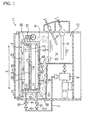
- Fig. 1 is a front explanatory section view, and is a section view in the direction of arrow along line I-I in Fig. 3.
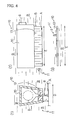
- Fig. 2 is also a front explanatory section view, and is a section view in the direction of arrow along line II-II section view Fig. 3.
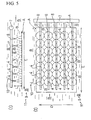
- Fig. 3 is an explanatory side view.
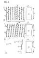
- Fig. 4-(1) is a side section view
- Fig. 4-(2) is a front view
- Fig. 4-(3) is a bottom view shown the many slit shaped injection orifices of the chemical solution injection equipment.
- Fig. 6-(1) is a schematic plan view of another example of slit shaped injection orifices of the chemical solution injection equipment
- Fig. 6-(2) is a schematic plan view of another example of spray nozzles of the chemical solution injection equipment
- Fig. 6-(3) is a schematic plan view of further another example of spray nozzles of the chemical solution injection equipment.
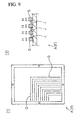
- Fig. 9-(1) is a plan explanatory view
- Fig. 9-2(2) is a front explanatory view providing an explanation of a printed circuit board (substrate).
- the printed circuit board F has all kinds of usage as the boards of all kinds of OA machines, boards for personal computers, boards of calculators and boards for all kinds of the other electronic machines along with the development of multimedia. Thus there are also variety of manufacturing procedures.
- the printed circuit board F is classified into one for all, single sided board, double sided board, multi-layered board(including the one made by recent build-up method) and flexible board. One of these recently is wound with the appearance of CSP, PBGA of the semiconductor chip package.
- the printed circuit board has significantly progressed in compact size, light weight, fineness, flexibility and multi-layers in recent years, especially in the super fineness, high precision and high density of circuits formed on the outer surfaces.
- the printed circuit board F e.g., is fabricated by the following. That is, the printed circuit board F uses printed circuit plate as its base material and is fabricated by sequentially and continuously executing many processes as ordering, layering, grinding, cutting; drilling, grinding and electroplating the holes for through hole usage; coating, drying or taping the etching resist; exposing the negative film for circuit usage; developing; etching; and peeling off the etching resist for circuit portions...etc.
- the two sides of insulation substrate as polyimide has executed the washing and grinding after the extended assembly of deposition by the hot press of copper foil.
- the executing soft etching to roughen the copper surface.
- the printed circuit board A of deposition plate by extending the two sided copper foils ahs cut into work sized pieces.
- the washing and two sides' grinding are executed, then the panel electroplating. Via this, the electroplating for the back wall of through hole is executed to make conduction between the out and back surfaces of circuit G.
- the printed circuit board A executes washing, grinding, washing and drying once more. Then, the membrane painting process for the light sensitive resist etching resist (i.e. the protective membrane with alkali-resitivity and acid-resitivity) is executed by painting to dry.
- the membrane painting process for the light sensitive resist etching resist i.e. the protective membrane with alkali-resitivity and acid-resitivity
- this light sensitive resist is hardened, and leave the copper portion of circuit G which is over-coated and protected by executing the cleaning and drying of the printed circuit board A.
- the unwanted portion of copper by solving and removing the foregoing light sensitive resist, is solved, removed and etched by the injection of the etching chemical solution of chemical solution B (also referred to the following description Fig. 1 and Fig. 3).
- Printed circuit board F e.g. has the dimensions (length by width) of 550 millimeters (mm) by (X) 550 millimeters (mm), 500mm X 500mm or 500mm X 300mm. Its thickness, e.g. is 0.06mm in the insulated substrate portion.
- the circuit G potion made of copper can reach as thin as 0.018mm thickness.
- the thickness of a whole body for this printed circuit board F is from 1 mm to 0.8mm, further can be 0.4mm, such that can achieve the super thinness.
- circuit width H can reach the range from 150 microns to 70 microns, even more to 40 microns, and has a tendency to achieve super fineness.
- the circuit width H of 20 microns also appears to have about 30 microns of knees in the space J between circuits.
- the printed circuit board F fabricated by this procedure is related to be formed by the post processing procedure which forms one of this manufacturing procedure, and is used to form a protective membrane of the formed circuit G.
- the painting membrane process is executed by the painting and drying of the solder resisted light sensitive resist. Then, the exposing and developing for negative film is executed.
- the part mounting portion of through hole portion generally, only the patterned light sensitive resist is solved and removed to exposure (the procedures hereof uses the foregoing procedures as standard).
- This circuit G is protected by the membrane which is formed in the light sensitive resist on the printed circuit board F. However, after this, the circuit G of the printed circuit board F is protected by pattern attaching which is executed corresponding to the mounting portion of parts.
- the printed circuit board F is fabricated by this procedure.
- the chemical solution treatment equipment as this developing device and etching device are, e.g., used for manufacturing procedures as the developing procedure and etching procedure of the foregoing printed circuit board F.
- the developing chemical solution and etching chemical solution of chemical solution B are injected to the thin plate shaped substrate of the printed circuit board A which is transported horizontally by a conveyer 2. Further, the chemical processing and chemical solution treatment as developing and etching are executed to form the circuit on the outer surface of printed circuit board A.
- the chemical solution treatment equipment as shown in Fig. 1, Fig. 2, Fig. 3 have the injected chemical solution B and the chemical solution tank 9 filled with the same chemical solution B; the conveyer 2 used for transporting the substrate of the printed circuit board A which is arranged in the chemical solution B of chemical solution tank 9; and the chemical solution injecting device 10 injecting the fresh chemical solution B toward the transported substrate of printed circuit board A which is arranged in the chemical solution B of chemical solution tank 9.
- the chemical solution tank 9 is mounted in the upper portion of processing chambers 11 as developing chamber and etching chamber, and the reservoir 12 is mounted in the lower portion of processing chamber 11.
- the chemical solution B injected from the spray nozzle 4 (the example in Fig. 5) and the slit shaped injecting orifice 13 (the example in Fig. 1, Fig. 2, Fig. 3 and Fig. 4) are flown down from chemical solution managing reservoir 12 due to the overflow from chemical solution tank 9, and recovered after being flown through the outer surface of printed circuit board A.
- the chemical solution B tarried in the chemical solution managing reservoir 12 executes this concentration management and temperature management, and uses a re-pump 6, a out pipe of main pipe 7 and the piping 8 manifolded from main pipe 7 as the interface press and feed toward the spray nozzle 4 of chemical solution injecting device 10 and slit shaped injecting orifice 13 for recycling.
- the heater is mounted in the chemical solution managing reservoir.
- the 15 is a concentration sensor of the chemical solution B.
- the 16 is the pressure adjusting valve mounted in piping 8.
- the chemical solution managing reservoir 12 is not in the lower portion of processing chamber 11 shown in these figures. But it also can be set in a location with lower height than that of a chemical solution tank 9 within the processing chamber 11. The whole layout of chemical solution treatment equipment becomes this kind.
- the conveyer 2 of chemical solution treatment equipment is description.
- the conveyer 2 located in the chemical solution treatment equipment shown in Fig.2, Fig. 3 are provided with multiple up-down rollers 3 and wheels (not shown in figures).
- the substrate of printed circuit board A is clamped and transported horizontal in transporting direction.
- the conveyer 2 is mounted in the chemical solution B of chemical solution tank 9.
- Several or many shafts 17 arranged horizontal in fix-spaced pitch are in the front-rear transporting direction D which is parallel with the left-right width direction E.
- the roller 3 mounted on each shaft 17 is prepared.
- roller 3 mounted on each shaft 17 is up-down arranged oppositely to clamp the printed circuit board A.
- the upper sided (lower sided) shaft 17 and roller 3 are rotated drive.
- the lower sided (upper sided) shaft 17 and roller 3 function as pushing and preventing the snake motion.
- Fig. 18 is a conveyer frame with driving gear 19.
- the conveyer 2 becomes this kind.
- the chemical solution injecting device 10 of this chemical solution treatment equipment we describe the chemical solution injecting device 10 of this chemical solution treatment equipment. Further, the chemical solution injecting device 10 of Fig. 3 as those shown in Fig. 1 together with rollers and wheels of a conveyer 2 are arranged between the front-rear intervals K. The horizontally transported printed circuit board only exists in the up-down interval L and is arranged oppositely.
- roller 3 and wheels which is put in the chemical solution B of a chemical solution tank 9, are arranged in designated pitch in the front-rear transporting direction.
- the examples shown in drawings are put in a proper position where the space equal to one piece of front-rear interval K is formed. Then, the chemical solution injecting device 10 is arranged within this front-rear interval K.
- every 3 rollers together form these front-rear intervals K.
- the upper roller 3 and lower roller 3 together from this front-rear interval K.
- the upper front-rear interval K and lower front-rear interval K is formed by offset in rear-front of the up-down relative position.
- the many chemical solution injecting devices 10 are mounted between each front-rear interval K.
- the tip of this chemical solution injecting device (the upper end or lower end of spray nozzle 4 and slit shaped injection orifice 13) for the printed circuit board is under 10mm representatively, e.g., is positioned at about 5mm of the up-down interval L (the traditional example in foregoing description Fig. 7 becomes about 150mm). Still, the up-down interval L is ranged from 20mm to 1 mm, and can have all kinds of possible setting.
- the chemical solution injecting device 10 shown as examples in Fig. 1, Fig. 2, Fig. 3 and Fig. 4 uses many slit shaped injecting orifices 13.
- This slip shaped orifice 13 is different from the spray nozzle 4 used in this traditional example foregoing description in Fig. 7. Corresponding to the substrate of transported printed circuit board A, it covers the left-right wide direction but not front-rear transportation direction D. And, it is arranged oppositely in the chemical solution B of chemical solution tank 9.
- the chemical solution injecting device 10 as shown in Fig. 4 has one end been connected with the piping 8 and the other end been closed.
- the hollow pipe body 20 is arranged along the wide direction E, and has the very thin front-rear gap formed as slit shaped orifice 13 is which is the lower end center line (thing in upper side) or upper end center line (thing is lower line) of the pipe body 20.
- This slit shaped orifice 13 has no fine front-rear gap and the linear gap and groove; its transportation direction D is not along the front-rear direction but along left-right wide direction E; and is arranged in a chemical solution tank 9. And, when the printed circuit board A is arranged in an upper position, the up-down interval L between lower end and the upper surface of printed circuit bas plate is set to be about 10mm. When the printed circuit board A is arranged in an upper position, the up-down interval L between upper end and the lower surface of printed circuit board is set to be under 10mm.
- the slit shaped orifice 13 and chemical solution injecting device 10 shown in Fig.3 and Fig.1, Fig.2 is that the printed circuit board is oppositely up-down arranged.
- the designated front-rear interval K is formed. This formed front-rear interval K also considers the arrangement of chemical solution injecting device 10 with slit shaped injection orifice.
- the slit shaped orifice 13 and chemical solution injecting device 10 shown in Fig. 3 is separately put in up-down and exists the intervals in transportation direction D by the odd numbered arrangement.
- it is also possible to be arranged one by one is also possible to be arranged one by one at only one location for up-down roller 3. That is, the front-rear interval K is formed only in one location in up-down roller 3.
- the chemical solution injection device as slit shaped injection orifice 13 is also possible is arranged separately one by one.
- the slit shaped orifice 13 and chemical solution injecting device 10 shown in Fig.3 and Fig.1, Fig.4 is one by one set with one long front-rear interval K separately in left-right wide direction E.
- those shown as Fig.6-(1), e.g., is also possible to be divided into 3 short intervals separately in left-right wide direction E.
- each ends of the divided each slit shaped injecting orifice 13 and chemical solution injection device 10 is connected with the ends of piping 8 which is manifolded.
- the slit shaped orifice 13 and chemical solution injecting device 10 shown in Fig.4 is that However, these drawing examples has certain inclination in front-rear corresponding to left-right wide direction E. It is also good to be arranged as the slit shaped orifice 13 and chemical solution injecting device 10.
- the slit shaped orifice 13 and chemical solution injecting device 10 shown in Fig.3, Fig.4 is that the injection angle corresponding to printed circuit board A is set to squared angle.
- the slit shaped orifice 13 has the angle setting to inject the curtain shaped chemical solution B from longitudinal direction.
- the injecting angle corresponding to printed circuit board A is possible to be set as with certain inclination in front-rear from an square angle.
- the curtain shaped chemical solution B is also possible to be injected to the printed circuit board by a inclined injecting angle in front-rear slanted direction slightly from square angle.
- This inclined injecting angle is set to only some angle, e.g., is set to about an injecting angle of 5 degrees. It is also possible to have its lower limit as 1-2 degrees, as for the upper limit is about 10 degrees.
- the slit shaped orifice 13 which is inclined in the down stream side of transportation direction D, has an incident angle to printed circuit board which is set to an obtuse angle in upstream side and acute angle in downstream side. Or contrary to this, it is also good to have an incident angle to printed circuit board which is set to an acute angle in upstream side and an obtuse angle in downstream side.
- the up-down interval L between the slit shaped orifice 13 of chemical solution injecting device 10 and printed circuit board A is less than 10mm, e.g., is set to 5mm.
- This up-down interval L also considers to be variant.
- the horizon printed circuit board A with certain levels is used in solution injection device 10, the level of chemical solution injecting device 10 and slit shaped injecting orifice is changeable.
- the up-down interval L can be changed to 3mm, 4mm, 5mm, 6mm, 7mm, and will be considered.
- the spray nozzles for the chemical solution device 10 is description.
- the chemical solution injection device 10 the height level of slit shaped injection orifice.
- Fig.1, Fig. 2, Fig. 3, Fig. 4-(1). Fig. 4-(2), Fig. 3-(1), Fig. 6-(1) according to the spray nozzle Fig. 5-(1), (2), Fig. 6-(1), (2) is also possible to use spray nozzle 4.
- this spray nozzle 4 corresponding the transported printed circuit board A is the same as the traditional example of the foregoing description Fig. 7 to totally cover a wide area of the front-rear transportation direction D and left-right wide direction E, and one by one is put in left-right with a designated interval pitch and oppositely arranged. It is different from the foregoing description traditional example of Fig.7. It is oppositely arranged in the chemical solution B of the chemical solution tank 9.
- This spray nozzle 4 is further description in detail.
- This chemical solution injection device 10 is shown as Fig.5, which has one end to be manifold-connected with main pipe 7 and the other end to be closed separately; the multiple piping 8 to be parallel in wide direction E (spray pipe, injection type) and the multiple piping 8 has the spray nozzles 4 to be formed in multiple by designated interval pitch.
- This spray nozzle 4 is rotated by a square angle from the front-rear transportation direction D to left-right wide direction E, then one-by-one put by designated pitch interval in front-rear-left-right and arranged by large numbers in the chemical solution tank 9.
- the provided chemical solution B is put in chemical solution B of the chemical solution tank 9, and is diffused and sprayed to transported printed circuit board from each spray nozzle 4.
- the slit shaped orifice 13 protruded from the chemical injection device 10 is arranged at front-rear interval K formed by every the 3 rollers along the transportation direction D.
- the spray nozzle 4 and the chemical injection device 10 and single or multiple piping 8 of the chemical solution injection device 10 and more the spray nozzles 4 are arranged at each front-rear interval K formed by lesser rollers, e.g. every 1 and 2.
- spray nozzle 4 in this listed document like the above description (multiple injection pipe type) is a hole and formed one in piping 8, and of course is included.
- the arrangement direction of piping 8 relative to wide direction D is the front-rear slant type, and the spray nozzle 4 formed in each piping 8 as shown in Fig. 6-(3) is also possible to be the one with gradually shift type in wide direction between each piping 8.
- this type of arrangement for the piping 8 along the front-rear transportation direction D is also possible(drawing is now shown).
- the spray nozzle 4 is as this.
- This chemical solution treatment equipment is used in, e.g. the manufacturing engineering of the printed circuit board. It comprises that the conveyer 2 which clamps the substrate of such printed circuit board A between the up-down multiple rollers 3 and wheel and transports them horizontally, the corresponding substrate of such printed circuit board A which is transported in conveyer 2, and the chemical solution injection device 10 which injects the chemical solution B as developing solution and etching solution (e.g. refer to Fig.1, Fig. 2, Fig.3).
- the chemical solution injecting device 10 is arranged at front-rear interval K of the roller 3 and wheel of conveyer 2. It is oppositely arranged at limited up-down interval L for the corresponding substrate of such printed circuit board A.
- the multiple oppositely arranged spray nozzle 4 covers the front-rear-left-right, or uses the oppositely arranged silt shaped orifice 13 to cover left-right (e.g. Fig.,4, further refer to Fig.1, Fig. 2, Fig. 3).
- Each spray nozzle 4 diffuses the chemical solution B in cone shape and wide end shape, and sprays then injects it.
- the silt shaped orifice 13 sprays the chemical solution B in straight-longitudinally curtain shape.
- this chemical solution treatment equipment is characterized by that it has this conveyer 2 and chemical solution injection device 10, and it is arrange in the chemical solution tank 9 filled with chemical solution B.
- this chemical solution treatment equipment is related to the substrate of printed circuit board A which is transported in the tarried chemical solution B in the chemical solution tank 9 on the conveyer.
- the fresh chemical solution B is injected through the chemical injection device 10 that is in the tarried solution B of the same chemical solution tank 9. Via this, the fresh chemical solution B is injected in the tarried solution B but not in the environment.
- the chemical solution treatment equipment as this for the substrate of printed circuit board, the chemical processing and chemical solution treatment such as developing and etching is executed by using the chemical solution like developing solution and etching solution.
- the expected circuit G is formed on its outer surface.
- this chemical solution treat equipment has the chemical solution tank 9 in the upper portion of its processing chamber 11.
- the chemical managing reservoir is arranged in the lower portion of its processing chamber 11.
- the 21 in Fig.1, Fig. 2 is a cover of processing chamber 11.
- the chemical solution B is injected from chemical injection device 10. And, the overflowed chemical solution B from the chemical solution tank 9 is flown down to the chemical solution injection device 10 for recovery. Further, the chemical solution B tarried in the chemical managing reservoir 12 is flown through the pipes such as pump 6, main pipe 7 and piping 8, press fed toward chemical injecting device 10 for recycling usage.
- the chemical solution treatment equipment has the following first, second, third, fourth, fifth, sixth and seventh kinds.
- this chemical solution treatment equipment injects the fresh chemical solution B from the chemical solution injection device 10 such as slit shaped injection orifice 13 and spray nozzle 4 which is in the chemical solution B of the same chemical solution tank 9, to the transported substrate of printed circuit board A which is in the tarried chemical solution B of chemical solution tank 9 of the processing chamber 11.
- the chemical solution injection device 10 such as slit shaped injection orifice 13 and spray nozzle 4 which is in the chemical solution B of the same chemical solution tank 9
- the transported substrate of printed circuit board A which is in the tarried chemical solution B of chemical solution tank 9 of the processing chamber 11.
- the phenomena such as the density of the fresh chemical solution B at middle portion of printed circuit board A is low and the amount is small, and the density of the fresh chemical solution B at left-right portion of printed circuit board A is high and the amount is large can be avoided.
- the chemical processing and chemical solution treatment like developing and etching by chemical solution which separately pass the middle portion and left-right side portion can be uniformed, the chemical processing and chemical solution treatment speed in the middle portion is slow in speeded or insufficient, and the chemical processing and chemical solution treatment at left-right side portion is too early, over advanced.
- the fresh chemical solution B is injected in the tarried chemical solution B and not in the environment.
- the phenomena as the injected chemical solution B flown to the left-right wide direction E (refer to Fig. 8-(2)) on the outer surface such as surface and back surface of the printed circuit board A can be really eliminated.
- the chemical solution tank 9 is mounted in the upper portion of processing chamber 11. And it is configured by the arrangement of the traditional used conveyer 2 which uses the roller 3 and wheel, and the chemical solution injection device 10 which uses multiple spray nozzle 4 or slot shaped orifice 13.
- this chemical solution treatment equipment has comparably simple configuration. It can fulfill the uniformity in the above description first and chemical processing and chemical solution treatment easily and really.
- the solution injecting device 10 such as the spray nozzle 4 and slit shaped orifice 13 in this chemical solution treatment equipment, is put in the chemical solution tank 9 and arranged between the front-rear interval K of rollers 3 and wheels of a conveyer 2. Further, corresponding to the transported printed circuit board A, e.g., it is oppositely arranged only within about 5mm.
- the injected fresh chemical solution B to the outer surface of surface and back surface of transported printed circuit board in the chemical solution B tarried in the chemical solution tank 9, can directly, effectively be injected along with impact. Further, the chemical processing and chemical solution treatment of developing and etching can be totally smoothly executed without particular slow in speed, thus the processing capability can be upgraded.
- the printed circuit board A put in this chemical solution treatment equipment is clamped between the up-down each rollers 3 and wheels of conveyer 2 for transportation, and use the floating force of the chemical solution B tarried in chemical solution tank 9 to transport the PCB between the front-rear each roller 3 and front-rear-left-right wheel under floating status.
- the fresh chemical solution B is injected from the chemical solution injecting device 10, such as the spray nozzle 4 and slit shaped orifice 13 in the chemical solution B which is stored in the same tank 9, to the transported printed circuit board A in the chemical solution B which is stored in the same tank 9.
- the chemical solution injecting device 10 such as the spray nozzle 4 and slit shaped orifice 13 in the chemical solution B which is stored in the same tank 9
- the chemical solution B is diffused in cone shape of gradually widened shape and injected through each spray nozzle 4. If there is non-uniform injection to the outer surface of printed circuit board A, it is easy to create the difference between interior and exterior as density, injection pressure and injection amount. ⁇ lt creates the locations of square angled injection to the printed circuit board A, and the locations of angled injection from side. From this aspect, it is difficult to become totally uniformed injection, the total injection pressure becomes low owing to diffusing and the impact becomes insufficient, thus the processing capability become low.
- the slit shaped orifice 13 as the chemical solution injecting device 10, they are arranged to cover the wide direction E.
- the chemical solution B barely diffuses toward the full width of the outer surface of printed circuit board A. Owing to the injection in slightly flat curtained type without diffusion straightly and vertically, (1) there is no desultoriness of injected chemical solution B and can be unified, (2) there is no accompanying of injection angle for chemical solution B, (3) it can be injected directly with high shooting pressure.
- the uniformity and processing capability of chemical processing and chemical solution treatment can be upgraded.
- the conveyer 2 is very essential for the transportation of substrate of printed circuit board A in the chemical solution B of tank 9.
- the solution injection device 10 as spray nozzle 4 and slit shaped injecting orifice in the chemical solution B of tank 9 are also very essential to emit a jet of the fresh chemical solution B to the substrate of printed circuit A.
- Part of the conveyer 2 and solution injection device 10 can also be arranged in the environment and not in the chemical solution B of the tank 9.
- the chemical solution treatment equipment such as developing and etching devices related to the present invention is described as above.
- the printed circuit board is transported through a conveyer, then the fresh chemical solution is injected via the chemical injection device such as spray nozzles or slit-typed injecting orifices. Therefore, the following effects can be achieved.
- the chemical solution is injected in the environment, the tarry of the injected dense chemical solution in the upper middle portion of a substrate of the printed circuit board can be really dismissed without encumbering the replacement of the injected fresh chemical solution, and the function degradation and tarry of the old chemical solution can be debarred.
- the upper middle portion, two side portions of upper surface, and the outer surface of back surface of the printed circuit board has totally be unified through the chemical processing and chemical solution treatment such as developing and etching, and there will be no slow in speed or insufficiency of the chemical processing and chemical solution treatment on the upper middle portion.
- the fresh chemical solution has been injected from the chemical solution injecting device in the chemical solution which is stored in the same tank.
- the chemical solution has been injected uniformly on the outer surface of the substrate of the transported printed circuit board.
- it can really prevent the chemical solution to flow in the left-right wide direction on the outer surface of the upper and back surfaces.
- the injected chemical solution flows in the left-right wide direction of the outer surface of the substrate of the printed circuit board and flows down from both left and right sides.
- the flown out is really removed by the executing of this injection in the chemical solution.
- low density and small amount of the fresh chemical solution in middle side and the high density and large amount of the fresh chemical solution in both left and right sides can also be prevented.
- the chemical processing and chemical solution treatment of developing and etching will become totally unified by the chemical solution treatment equipment of the present invention; the speed slow in speed in the chemical processing and chemical solution treatment of the outer surface of middle portion, and insufficiency; and the earliness and over improvement in the chemical processing and chemical solution treatment of two side portions will be solved, while the chemical solution passes through the middle portions and left-right two side portions.
- the chemical solution treatment equipment according to the present invention By the chemical solution treatment equipment according to the present invention, the slow in speed of chemical processing and chemical solution treatment, insufficiency and over-excessiveness in the above description first and second kinds will not occur and the uniformity in chemical processing and chemical solution treatment can be achieved.
- the CSP, PBGA of package windings of semiconductor chips contains in the printed circuit board.
- the progress in the super fineness, high precision and high density of circuit is significant.
- the chemical solution treatment equipment according to the present invention it is possible to form a stable circuit width with uniformity even in a super fine circuit width. This means a lot that the limit value of circuit width can be significantly rewritten.
- the chemical solution treatment equipment of the present invention even the printed circuit board with a circuit width of 20 microns and space between circuits of 30 microns can be manufactured easily.
- this chemical solution treatment equipment can simply and really realize better uniformity in the above description 1st and 2nd chemical processing and chemical solution treatment by a simple structure set in the chemical solution tank, while comparing with the conveyer which using the conventional roller and wheel and the chemical solution injecting device which using the spray nozzle and slit shaped injecting orifice.
- the above description traditional chemical solution treatment equipment can save up to 30% of the total equipment cost and is very excellent in the equipment cost aspect while comparing the situations such as each nozzle attached to the left-right swung mechanism and oscillation mechanism, and the transported printed circuit board attached to the up-down reverse mechanism and left-right turn mechanism. Further, compared with the traditional chemical solution treatment equipment, it is also good in the setup space aspect.
- the injecting devices as spray nozzles and slit shaped injecting orifices in the chemical solution tank are arranged in front-rear intervals between rollers and wheels of the conveyer.
- the substrate of the printed circuit board it is only arranged oppositely in up-down intervals.
- the chemical solution injecting device of the present invention can directly and effectively spray the fresh injected chemical solution and impact on the outer surface of the substrate of the printed circuit board which is transported and located in the chemical solution of the chemical solution tank, thus can smoothly renew the chemical solution on the outer surface of the substrate of the printed circuit board.
- the chemical processing and chemical solution treatment of developing and etching of the outer surface of the substrate of the printed circuit board can be executed without particular slow in speed, such that the processing capability, production efficiency is upgraded, and also the cost performance.
- this chemical solution treatment equipment can spray the chemical solution from the chemical solution injecting devices, such as spray nozzles and slit shaped injecting orifices in the chemical solution of the same chemical solution tank, to the corresponding substrate of transported printed circuit board in the chemical solution of the same chemical solution tank of this chemical solution treatment equipment.
- the weight of tarried chemical solution which is injected and the bending up of from the substrate of the printed circuit board is really eliminated.
- the substrate of the printed circuit board located in the chemical solution injecting device of the present invention is clamped between each roller and wheel of the conveyer in the chemical solution of the chemical solution tank, and then is transported along with the front-rear rollers and front-rear-left-right wheels under the half floating status due to the floating force of the chemical solution in the chemical solution tank.
- the substrate of the printed circuit board slightly bent concavely due to the weight has no reverse bending, and can be transported smoothly as expected without obstacles,
- the chemical processing and chemical solution treatment of the substrate of the printed circuit board can be smoothly executed, such that it prevents the occurrence of defects, the staying becomes better and the productivity is upgrade.
- the developing chemical solution and etching chemical solution diffused, sprayed and injected from each spray nozzle of the chemical solution injecting devices, such as the foregoing traditional chemical solution treatment equipment will not be gasified in large amount. For example, the gasification of the vaporized oxidizer in the chemical solution is avoided.
- the exhausting mechanism which is used for exhausting the poisonous gas from the interior of processing chamber to its exterior is not necessary because of no occurrence of the poisonous gas which is hazardous to human body, such that the processing capability, production efficiency is upgraded, and also the cost performance.
Landscapes
- Engineering & Computer Science (AREA)
- Chemical & Material Sciences (AREA)
- Manufacturing & Machinery (AREA)
- Microelectronics & Electronic Packaging (AREA)
- Materials Engineering (AREA)
- Mechanical Engineering (AREA)
- Metallurgy (AREA)
- Organic Chemistry (AREA)
- Chemical Kinetics & Catalysis (AREA)
- General Chemical & Material Sciences (AREA)
- Manufacturing Of Printed Circuit Boards (AREA)
- Coating Apparatus (AREA)
- Chemically Coating (AREA)
- ing And Chemical Polishing (AREA)
- Spray Control Apparatus (AREA)
- Manufacturing Of Printed Wiring (AREA)
Priority Applications (3)
| Application Number | Priority Date | Filing Date | Title |
|---|---|---|---|
| JP11042744A JP3120073B2 (ja) | 1999-02-22 | 1999-02-22 | 薬液処理装置 |
| EP99305458A EP1067830A1 (fr) | 1999-02-22 | 1999-07-09 | Equipement pour le traitement avec une solution chimique |
| CN99121786.1A CN1131733C (zh) | 1999-02-22 | 1999-10-11 | 药液处理装置 |
Applications Claiming Priority (2)
| Application Number | Priority Date | Filing Date | Title |
|---|---|---|---|
| JP11042744A JP3120073B2 (ja) | 1999-02-22 | 1999-02-22 | 薬液処理装置 |
| EP99305458A EP1067830A1 (fr) | 1999-02-22 | 1999-07-09 | Equipement pour le traitement avec une solution chimique |
Publications (1)
| Publication Number | Publication Date |
|---|---|
| EP1067830A1 true EP1067830A1 (fr) | 2001-01-10 |
Family
ID=26153534
Family Applications (1)
| Application Number | Title | Priority Date | Filing Date |
|---|---|---|---|
| EP99305458A Withdrawn EP1067830A1 (fr) | 1999-02-22 | 1999-07-09 | Equipement pour le traitement avec une solution chimique |
Country Status (3)
| Country | Link |
|---|---|
| EP (1) | EP1067830A1 (fr) |
| JP (1) | JP3120073B2 (fr) |
| CN (1) | CN1131733C (fr) |
Families Citing this family (13)
| Publication number | Priority date | Publication date | Assignee | Title |
|---|---|---|---|---|
| KR100443373B1 (ko) * | 2001-12-28 | 2004-08-09 | 삼성전기주식회사 | 커버를 구비한 인쇄회로기판 분사용 노즐 |
| JP2006090712A (ja) * | 2004-09-21 | 2006-04-06 | Hiroshima Univ | 腐食試験装置 |
| KR100928951B1 (ko) * | 2008-06-09 | 2009-11-30 | 세메스 주식회사 | 케미컬 플로우 방법, 그리고 이를 이용하는 집적 회로소자의 제조 방법 및 장치 |
| JP2011009247A (ja) * | 2009-06-23 | 2011-01-13 | Sharp Corp | 太陽電池の製造方法及び湿式エッチング装置 |
| DE102010000211A1 (de) * | 2010-01-26 | 2011-07-28 | Atotech Deutschland GmbH, 90537 | Vorrichtung zum Transport von plattenförmigen Substraten in einer Anlage zur chemischen und/oder elektrochemischen Behandlung |
| JP2015084407A (ja) * | 2013-09-17 | 2015-04-30 | アイケイ株式会社 | 基板材の表面処理装置 |
| CN104320927B (zh) * | 2014-11-10 | 2017-08-08 | 浙江振有电子股份有限公司 | 带滚动式软毛刷的hdi印制线路板铜箔棕化装置 |
| JP6189279B2 (ja) * | 2014-11-14 | 2017-08-30 | 新光電気工業株式会社 | エッチング装置 |
| CN107709618B (zh) * | 2015-07-28 | 2019-08-27 | 东亚电子株式会社 | 用于金属导体的蚀刻的药液更新用喷嘴及蚀刻装置 |
| CN107434363A (zh) * | 2016-05-25 | 2017-12-05 | 东莞市腾明智能设备有限公司 | 电路板玻纤粗化装置 |
| CN111013879B (zh) * | 2020-01-10 | 2021-08-13 | 徐州鸿程铁艺装饰工程有限公司 | 一种镀锌后护栏用上色设备 |
| CN112367769B (zh) * | 2020-11-24 | 2021-06-15 | 广州泰华多层电路股份有限公司 | 一种电路板安全蚀刻器及其使用方法 |
| CN116828724B (zh) * | 2023-08-24 | 2023-11-21 | 深圳市国硕宏电子有限公司 | 一种用于pcb板蚀刻加工的退膜装置 |
Citations (9)
| Publication number | Priority date | Publication date | Assignee | Title |
|---|---|---|---|---|
| DE3204912C1 (de) * | 1982-02-12 | 1983-08-11 | Fritz Dipl.-Ing. 8000 München Knollmann | Vorrichtung zum Auswaschen belichteter Druckplatten, insbesondere dünner Kunststoffdruckplatten |
| EP0212253A2 (fr) * | 1985-08-06 | 1987-03-04 | ATOTECH Deutschland GmbH | Procédé et dispositif de nettoyage, d'activation et/ou de métallisation de trous dans des plaquettes de circuit transportées horizontalement |
| EP0254961A1 (fr) * | 1986-07-28 | 1988-02-03 | Siemens Aktiengesellschaft | Installation de traitement en particulier des plaques de circuits imprimés se déplaçant horizontalement |
| JPH04107278A (ja) * | 1990-08-27 | 1992-04-08 | Matsushita Electric Ind Co Ltd | 湿式エッチング装置 |
| WO1993001699A1 (fr) * | 1991-07-02 | 1993-01-21 | Egeland Bjoern | Procede de nettoyage de cartes de circuits imprimes et appareil associe |
| US5192394A (en) * | 1991-12-16 | 1993-03-09 | International Business Machines Corporation | Fluid treatment apparatus and method |
| JPH06108297A (ja) * | 1991-10-08 | 1994-04-19 | Tokyo Kakoki Kk | 化学処理装置 |
| DE29511549U1 (de) * | 1995-07-20 | 1995-09-07 | Pill e.K., 71549 Auenwald | Vorrichtung zur Oberflächenbehandlung von Leiterplatten |
| DE19519211A1 (de) * | 1995-05-25 | 1996-11-28 | Hoellmueller Maschbau H | Verfahren zur Behandlung von Gegenständen, insbesondere von elektronischen Leiterplatten, sowie Vorrichtung zur Durchführung dieses Verfahrens |
-
1999
- 1999-02-22 JP JP11042744A patent/JP3120073B2/ja not_active Expired - Fee Related
- 1999-07-09 EP EP99305458A patent/EP1067830A1/fr not_active Withdrawn
- 1999-10-11 CN CN99121786.1A patent/CN1131733C/zh not_active Expired - Fee Related
Patent Citations (9)
| Publication number | Priority date | Publication date | Assignee | Title |
|---|---|---|---|---|
| DE3204912C1 (de) * | 1982-02-12 | 1983-08-11 | Fritz Dipl.-Ing. 8000 München Knollmann | Vorrichtung zum Auswaschen belichteter Druckplatten, insbesondere dünner Kunststoffdruckplatten |
| EP0212253A2 (fr) * | 1985-08-06 | 1987-03-04 | ATOTECH Deutschland GmbH | Procédé et dispositif de nettoyage, d'activation et/ou de métallisation de trous dans des plaquettes de circuit transportées horizontalement |
| EP0254961A1 (fr) * | 1986-07-28 | 1988-02-03 | Siemens Aktiengesellschaft | Installation de traitement en particulier des plaques de circuits imprimés se déplaçant horizontalement |
| JPH04107278A (ja) * | 1990-08-27 | 1992-04-08 | Matsushita Electric Ind Co Ltd | 湿式エッチング装置 |
| WO1993001699A1 (fr) * | 1991-07-02 | 1993-01-21 | Egeland Bjoern | Procede de nettoyage de cartes de circuits imprimes et appareil associe |
| JPH06108297A (ja) * | 1991-10-08 | 1994-04-19 | Tokyo Kakoki Kk | 化学処理装置 |
| US5192394A (en) * | 1991-12-16 | 1993-03-09 | International Business Machines Corporation | Fluid treatment apparatus and method |
| DE19519211A1 (de) * | 1995-05-25 | 1996-11-28 | Hoellmueller Maschbau H | Verfahren zur Behandlung von Gegenständen, insbesondere von elektronischen Leiterplatten, sowie Vorrichtung zur Durchführung dieses Verfahrens |
| DE29511549U1 (de) * | 1995-07-20 | 1995-09-07 | Pill e.K., 71549 Auenwald | Vorrichtung zur Oberflächenbehandlung von Leiterplatten |
Non-Patent Citations (2)
| Title |
|---|
| PATENT ABSTRACTS OF JAPAN vol. 16, no. 351 (C - 0968) 29 July 1992 (1992-07-29) * |
| PATENT ABSTRACTS OF JAPAN vol. 18, no. 392 (C - 1228) 22 July 1994 (1994-07-22) * |
Also Published As
| Publication number | Publication date |
|---|---|
| CN1264626A (zh) | 2000-08-30 |
| JP2000237649A (ja) | 2000-09-05 |
| CN1131733C (zh) | 2003-12-24 |
| JP3120073B2 (ja) | 2000-12-25 |
Similar Documents
| Publication | Publication Date | Title |
|---|---|---|
| KR100713235B1 (ko) | 박판재(薄板材)의 표면처리장치 | |
| KR20100123638A (ko) | 기판재의 표면 처리 장치 | |
| JP3120073B2 (ja) | 薬液処理装置 | |
| JP4626068B2 (ja) | エッチング方法およびエッチング装置 | |
| US7758716B2 (en) | Apparatus for spraying etchant solution onto preformed printed circuit board | |
| JP5166367B2 (ja) | 基板材の表面処理装置 | |
| TWM553329U (zh) | 卷對卷非接觸式膠體金屬化學鍍設備 | |
| JP2003200090A (ja) | 印刷回路基板用の噴射ノズルおよびこれを用いたウェットライン設備 | |
| JP2006332300A (ja) | メッキ基板のエッチング装置 | |
| JP3981874B2 (ja) | 薬液処理方法および薬液処理装置 | |
| KR20160017589A (ko) | 기판재의 표면 처리 장치 | |
| CN102196672B (zh) | 电路板制作方法 | |
| JP2004214490A (ja) | 洗浄装置 | |
| JP2005232494A (ja) | 基板材の表面処理装置 | |
| EP0967845A1 (fr) | Injecteur de liquide | |
| JP3181884B2 (ja) | 薬液処理装置 | |
| JP3398345B2 (ja) | 薬液噴射装置 | |
| US6344106B1 (en) | Apparatus, and corresponding method, for chemically etching substrates | |
| JP4223121B2 (ja) | 電子装置用シャワー噴射装置及びシャワー噴射方法 | |
| JP2004313827A (ja) | 表面処理装置 | |
| KR102260571B1 (ko) | 회전형 수직 습식에칭장치 | |
| JPH0116037B2 (fr) | ||
| KR101052953B1 (ko) | 기판 처리 방법 | |
| JPH0372088A (ja) | スプレー処理装置 | |
| KR100889797B1 (ko) | 케미컬 분사 방법 및 장치 |
Legal Events
| Date | Code | Title | Description |
|---|---|---|---|
| PUAI | Public reference made under article 153(3) epc to a published international application that has entered the european phase |
Free format text: ORIGINAL CODE: 0009012 |
|
| 17P | Request for examination filed |
Effective date: 20000630 |
|
| AK | Designated contracting states |
Kind code of ref document: A1 Designated state(s): DE FR IT SE |
|
| AX | Request for extension of the european patent |
Free format text: AL;LT;LV;MK;RO;SI |
|
| AKX | Designation fees paid |
Free format text: DE FR IT SE |
|
| 17Q | First examination report despatched |
Effective date: 20040322 |
|
| STAA | Information on the status of an ep patent application or granted ep patent |
Free format text: STATUS: THE APPLICATION IS DEEMED TO BE WITHDRAWN |
|
| 18D | Application deemed to be withdrawn |
Effective date: 20041002 |