EP1069617A2 - Panneau à circuit imprimé à multi-couches - Google Patents
Panneau à circuit imprimé à multi-couches Download PDFInfo
- Publication number
- EP1069617A2 EP1069617A2 EP00114903A EP00114903A EP1069617A2 EP 1069617 A2 EP1069617 A2 EP 1069617A2 EP 00114903 A EP00114903 A EP 00114903A EP 00114903 A EP00114903 A EP 00114903A EP 1069617 A2 EP1069617 A2 EP 1069617A2
- Authority
- EP
- European Patent Office
- Prior art keywords
- power
- layer
- source
- wiring
- conductive pattern
- Prior art date
- Legal status (The legal status is an assumption and is not a legal conclusion. Google has not performed a legal analysis and makes no representation as to the accuracy of the status listed.)
- Withdrawn
Links
Images








Classifications
-
- H—ELECTRICITY
- H05—ELECTRIC TECHNIQUES NOT OTHERWISE PROVIDED FOR
- H05K—PRINTED CIRCUITS; CASINGS OR CONSTRUCTIONAL DETAILS OF ELECTRIC APPARATUS; MANUFACTURE OF ASSEMBLAGES OF ELECTRICAL COMPONENTS
- H05K1/00—Printed circuits
- H05K1/02—Details
- H05K1/11—Printed elements for providing electric connections to or between printed circuits
- H05K1/111—Pads for surface mounting, e.g. lay-out
- H05K1/112—Pads for surface mounting, e.g. lay-out directly combined with via connections
- H05K1/114—Pad being close to via, but not surrounding the via
-
- H—ELECTRICITY
- H10—SEMICONDUCTOR DEVICES; ELECTRIC SOLID-STATE DEVICES NOT OTHERWISE PROVIDED FOR
- H10W—GENERIC PACKAGES, INTERCONNECTIONS, CONNECTORS OR OTHER CONSTRUCTIONAL DETAILS OF DEVICES COVERED BY CLASS H10
- H10W70/00—Package substrates; Interposers; Redistribution layers [RDL]
- H10W70/60—Insulating or insulated package substrates; Interposers; Redistribution layers
- H10W70/611—Insulating or insulated package substrates; Interposers; Redistribution layers for connecting multiple chips together
-
- H—ELECTRICITY
- H10—SEMICONDUCTOR DEVICES; ELECTRIC SOLID-STATE DEVICES NOT OTHERWISE PROVIDED FOR
- H10W—GENERIC PACKAGES, INTERCONNECTIONS, CONNECTORS OR OTHER CONSTRUCTIONAL DETAILS OF DEVICES COVERED BY CLASS H10
- H10W70/00—Package substrates; Interposers; Redistribution layers [RDL]
- H10W70/60—Insulating or insulated package substrates; Interposers; Redistribution layers
- H10W70/62—Insulating or insulated package substrates; Interposers; Redistribution layers characterised by their interconnections
- H10W70/63—Vias, e.g. via plugs
- H10W70/635—Through-vias
-
- H—ELECTRICITY
- H10—SEMICONDUCTOR DEVICES; ELECTRIC SOLID-STATE DEVICES NOT OTHERWISE PROVIDED FOR
- H10W—GENERIC PACKAGES, INTERCONNECTIONS, CONNECTORS OR OTHER CONSTRUCTIONAL DETAILS OF DEVICES COVERED BY CLASS H10
- H10W70/00—Package substrates; Interposers; Redistribution layers [RDL]
- H10W70/60—Insulating or insulated package substrates; Interposers; Redistribution layers
- H10W70/62—Insulating or insulated package substrates; Interposers; Redistribution layers characterised by their interconnections
- H10W70/65—Shapes or dispositions of interconnections
-
- H—ELECTRICITY
- H05—ELECTRIC TECHNIQUES NOT OTHERWISE PROVIDED FOR
- H05K—PRINTED CIRCUITS; CASINGS OR CONSTRUCTIONAL DETAILS OF ELECTRIC APPARATUS; MANUFACTURE OF ASSEMBLAGES OF ELECTRICAL COMPONENTS
- H05K1/00—Printed circuits
- H05K1/02—Details
- H05K1/0286—Programmable, customizable or modifiable circuits
- H05K1/0287—Programmable, customizable or modifiable circuits having an universal lay-out, e.g. pad or land grid patterns or mesh patterns
- H05K1/0289—Programmable, customizable or modifiable circuits having an universal lay-out, e.g. pad or land grid patterns or mesh patterns having a matrix lay-out, i.e. having selectively interconnectable sets of X-conductors and Y-conductors in different planes
-
- H—ELECTRICITY
- H05—ELECTRIC TECHNIQUES NOT OTHERWISE PROVIDED FOR
- H05K—PRINTED CIRCUITS; CASINGS OR CONSTRUCTIONAL DETAILS OF ELECTRIC APPARATUS; MANUFACTURE OF ASSEMBLAGES OF ELECTRICAL COMPONENTS
- H05K1/00—Printed circuits
- H05K1/02—Details
- H05K1/11—Printed elements for providing electric connections to or between printed circuits
- H05K1/115—Via connections; Lands around holes or via connections
-
- H—ELECTRICITY
- H05—ELECTRIC TECHNIQUES NOT OTHERWISE PROVIDED FOR
- H05K—PRINTED CIRCUITS; CASINGS OR CONSTRUCTIONAL DETAILS OF ELECTRIC APPARATUS; MANUFACTURE OF ASSEMBLAGES OF ELECTRICAL COMPONENTS
- H05K2201/00—Indexing scheme relating to printed circuits covered by H05K1/00
- H05K2201/09—Shape and layout
- H05K2201/09209—Shape and layout details of conductors
- H05K2201/095—Conductive through-holes or vias
- H05K2201/09627—Special connections between adjacent vias, not for grounding vias
-
- H—ELECTRICITY
- H05—ELECTRIC TECHNIQUES NOT OTHERWISE PROVIDED FOR
- H05K—PRINTED CIRCUITS; CASINGS OR CONSTRUCTIONAL DETAILS OF ELECTRIC APPARATUS; MANUFACTURE OF ASSEMBLAGES OF ELECTRICAL COMPONENTS
- H05K2201/00—Indexing scheme relating to printed circuits covered by H05K1/00
- H05K2201/09—Shape and layout
- H05K2201/09209—Shape and layout details of conductors
- H05K2201/09654—Shape and layout details of conductors covering at least two types of conductors provided for in H05K2201/09218 - H05K2201/095
- H05K2201/09709—Staggered pads, lands or terminals; Parallel conductors in different planes
-
- H—ELECTRICITY
- H05—ELECTRIC TECHNIQUES NOT OTHERWISE PROVIDED FOR
- H05K—PRINTED CIRCUITS; CASINGS OR CONSTRUCTIONAL DETAILS OF ELECTRIC APPARATUS; MANUFACTURE OF ASSEMBLAGES OF ELECTRICAL COMPONENTS
- H05K2201/00—Indexing scheme relating to printed circuits covered by H05K1/00
- H05K2201/09—Shape and layout
- H05K2201/09818—Shape or layout details not covered by a single group of H05K2201/09009 - H05K2201/09809
- H05K2201/09854—Hole or via having special cross-section, e.g. elliptical
-
- H—ELECTRICITY
- H05—ELECTRIC TECHNIQUES NOT OTHERWISE PROVIDED FOR
- H05K—PRINTED CIRCUITS; CASINGS OR CONSTRUCTIONAL DETAILS OF ELECTRIC APPARATUS; MANUFACTURE OF ASSEMBLAGES OF ELECTRICAL COMPONENTS
- H05K2201/00—Indexing scheme relating to printed circuits covered by H05K1/00
- H05K2201/10—Details of components or other objects attached to or integrated in a printed circuit board
- H05K2201/10613—Details of electrical connections of non-printed components, e.g. special leads
- H05K2201/10621—Components characterised by their electrical contacts
- H05K2201/10674—Flip chip
-
- H—ELECTRICITY
- H10—SEMICONDUCTOR DEVICES; ELECTRIC SOLID-STATE DEVICES NOT OTHERWISE PROVIDED FOR
- H10W—GENERIC PACKAGES, INTERCONNECTIONS, CONNECTORS OR OTHER CONSTRUCTIONAL DETAILS OF DEVICES COVERED BY CLASS H10
- H10W90/00—Package configurations
- H10W90/701—Package configurations characterised by the relative positions of pads or connectors relative to package parts
- H10W90/721—Package configurations characterised by the relative positions of pads or connectors relative to package parts of bump connectors
- H10W90/724—Package configurations characterised by the relative positions of pads or connectors relative to package parts of bump connectors between a chip and a stacked insulating package substrate, interposer or RDL
Definitions
- each of the 1aM layer, the 2aM layer, the 4aM layer, the 5aM layer, and the 7aM layer acts as a signal layer.
- Each of the 0aM layer, the 3aM layer, and the 6aM layer acts as the grounding layer.
- the 8aM layer acts as a cover surface layer.
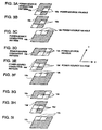
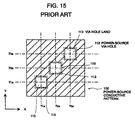
- a power-source conductive pattern 100a with power-source via holes 112 is formed on each of the 8aM layer, the 7aM layer, the 4am layer, and the 1aM.
- a power-source conductive pattern 100b is formed on each of the 6aM layer, the 3aM layer, and the 0aM layer.
- a power-source conductive pattern 100c is formed on each of the 5aM layer and the 2aM layer.
- the power-source via holes 112a to 112c are positioned in such a way that the projected positions of the power-source via holes 112a to 112c are not aligned with each other when the power-source conductive patterns 100a to 100c are piled up.
- both the power-source via hole 112b formed on the power-source conductive pattern 100b and the power-source via hole 112c formed on the power-source conductive pattern 100c are not electrically connected to the power-source via hole 112a in the power-source conductive pattern 100a because the power-source via hole 112a is arranged as shown in the above example.
- FIG. 19 is a plan view schematically and partially illustrating a conventional build-up board.
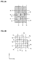
- FIG. 1A is a plan view illustrating a polyimide/ceramic multilayer wiring board according to a first embodiment of the present invention.
- FIG. 1B is a cross-sectional view schematically illustrating the polyimide/ceramic multilayer wiring board taken along the line A-A of FIG. 1A.
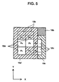
- the line segments X 1 , X 2 and X 3 and the line segments Y 1 , Y 2 and Y 3 shown in FIG. 2B correspond to those in FIG. 2A, respectively.
- P 1 to P 9 respectively represent cross points between the line segments.
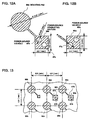
- Areas surrounded by solid lines in FIG. 2B represent power-source via holes 12a, 12a', 12b, and 12c.
- three power-source via holes 12 in FIG. 2A are formed at the positions p 1 , P 4 and p 5 shown in FIG. 2B, respectively.
- a via hole is not formed at the position P 9 .
- the present invention should not be limited to only this embodiment. If necessary, a via hole may be formed at the position P 9 .
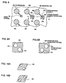
- Round mounting pads 86a and 86b are arranged at equal intervals, as shown in FIG. 8.
- the mounting pad 86a is electrically connected to two power-source via holes 87b for power supplying, which are formed on the square power-source conductive pattern 90b.
- the mounting pad 88b is electrically connected to the signal via hole 89 for signal transmission.
Landscapes
- Engineering & Computer Science (AREA)
- Microelectronics & Electronic Packaging (AREA)
- Production Of Multi-Layered Print Wiring Board (AREA)
Applications Claiming Priority (2)
| Application Number | Priority Date | Filing Date | Title |
|---|---|---|---|
| JP20375699A JP3562568B2 (ja) | 1999-07-16 | 1999-07-16 | 多層配線基板 |
| JP20375699 | 1999-07-16 |
Publications (2)
| Publication Number | Publication Date |
|---|---|
| EP1069617A2 true EP1069617A2 (fr) | 2001-01-17 |
| EP1069617A3 EP1069617A3 (fr) | 2004-11-03 |
Family
ID=16479326
Family Applications (1)
| Application Number | Title | Priority Date | Filing Date |
|---|---|---|---|
| EP00114903A Withdrawn EP1069617A3 (fr) | 1999-07-16 | 2000-07-14 | Panneau à circuit imprimé à multi-couches |
Country Status (3)
| Country | Link |
|---|---|
| US (1) | US6407343B1 (fr) |
| EP (1) | EP1069617A3 (fr) |
| JP (1) | JP3562568B2 (fr) |
Cited By (4)
| Publication number | Priority date | Publication date | Assignee | Title |
|---|---|---|---|---|
| WO2004017687A1 (fr) * | 2002-05-23 | 2004-02-26 | International Business Machines Corporation | Structure amelioree de trous d'interconnexion empiles dans des supports de dispositifs electroniques |
| US7240429B2 (en) | 2001-06-13 | 2007-07-10 | Denso Corporation | Manufacturing method for a printed circuit board |
| CN104377183A (zh) * | 2013-08-16 | 2015-02-25 | 台湾积体电路制造股份有限公司 | 用于多层金属布局的金属焊盘偏移 |
| EP4447622A4 (fr) * | 2022-04-24 | 2025-04-16 | Huawei Technologies Co., Ltd. | Dispositif électronique, et carte de circuit imprimé et son procédé de fabrication |
Families Citing this family (18)
| Publication number | Priority date | Publication date | Assignee | Title |
|---|---|---|---|---|
| US7259336B2 (en) | 2000-06-19 | 2007-08-21 | Nortel Networks Limited | Technique for improving power and ground flooding |
| US7725860B1 (en) | 2000-06-19 | 2010-05-25 | Herman Kwong | Contact mapping using channel routing |
| US7107673B2 (en) * | 2000-06-19 | 2006-09-19 | Nortel Networks Limited | Technique for accommodating electronic components on a multiplayer signal routing device |
| US7069646B2 (en) * | 2000-06-19 | 2006-07-04 | Nortel Networks Limited | Techniques for reducing the number of layers in a multilayer signal routing device |
| US7281326B1 (en) | 2000-06-19 | 2007-10-16 | Nortel Network Limited | Technique for routing conductive traces between a plurality of electronic components of a multilayer signal routing device |
| US7256354B2 (en) * | 2000-06-19 | 2007-08-14 | Wyrzykowska Aneta O | Technique for reducing the number of layers in a multilayer circuit board |
| US20040212103A1 (en) * | 2000-06-19 | 2004-10-28 | Herman Kwong | Techniques for pin arrangements in circuit chips |
| US6602078B2 (en) * | 2001-03-16 | 2003-08-05 | Cenix, Inc. | Electrical interconnect having a multi-layer circuit board structure and including a conductive spacer for impedance matching |
| JP3864093B2 (ja) * | 2002-01-10 | 2006-12-27 | シャープ株式会社 | プリント配線基板、電波受信用コンバータおよびアンテナ装置 |
| DE10205450A1 (de) * | 2002-02-08 | 2003-08-28 | Infineon Technologies Ag | Schaltungsträger und Herstellung desselben |
| US7405364B2 (en) * | 2002-12-30 | 2008-07-29 | Intel Corporation | Decoupled signal-power substrate architecture |
| US7167070B2 (en) * | 2003-09-01 | 2007-01-23 | Murata Manufacturing Co., Ltd. | Laminated coil component and method of producing the same |
| JP5201983B2 (ja) * | 2007-12-28 | 2013-06-05 | 富士通株式会社 | 電子部品 |
| TWI347810B (en) * | 2008-10-03 | 2011-08-21 | Po Ju Chou | A method for manufacturing a flexible pcb and the structure of the flexible pcb |
| KR20110113980A (ko) * | 2010-04-12 | 2011-10-19 | 삼성전자주식회사 | 필름을 포함한 다층 인쇄회로기판 및 그 제조 방법 |
| KR101218985B1 (ko) * | 2011-05-31 | 2013-01-04 | 삼성전기주식회사 | 칩형 코일 부품 |
| US9275925B2 (en) | 2013-03-12 | 2016-03-01 | Taiwan Semiconductor Manufacturing Company, Ltd. | System and method for an improved interconnect structure |
| US10244629B1 (en) * | 2017-11-03 | 2019-03-26 | Innovium, Inc. | Printed circuit board including multi-diameter vias |
Family Cites Families (14)
| Publication number | Priority date | Publication date | Assignee | Title |
|---|---|---|---|---|
| FR2512315A1 (fr) * | 1981-09-02 | 1983-03-04 | Rouge Francois | Ebauche de circuit electrique multicouche et procede de fabrication de circuits multicouches en comportant application |
| JPH023631Y2 (fr) * | 1984-12-28 | 1990-01-29 | ||
| US5288949A (en) * | 1992-02-03 | 1994-02-22 | Ncr Corporation | Connection system for integrated circuits which reduces cross-talk |
| US5410107A (en) * | 1993-03-01 | 1995-04-25 | The Board Of Trustees Of The University Of Arkansas | Multichip module |
| JPH06291216A (ja) * | 1993-04-05 | 1994-10-18 | Sony Corp | 基板及びセラミックパッケージ |
| US5378927A (en) * | 1993-05-24 | 1995-01-03 | International Business Machines Corporation | Thin-film wiring layout for a non-planar thin-film structure |
| JP3408590B2 (ja) * | 1993-09-29 | 2003-05-19 | 富士通株式会社 | 多層プリント基板の配線構造 |
| KR100194130B1 (ko) * | 1994-03-30 | 1999-06-15 | 니시무로 타이죠 | 반도체 패키지 |
| US5574630A (en) * | 1995-05-11 | 1996-11-12 | International Business Machines Corporation | Laminated electronic package including a power/ground assembly |
| JP3287181B2 (ja) * | 1995-08-15 | 2002-05-27 | ソニー株式会社 | 多層配線の接続構造 |
| JP3732927B2 (ja) * | 1997-07-31 | 2006-01-11 | 京セラ株式会社 | 多層配線基板 |
| US6175088B1 (en) * | 1998-10-05 | 2001-01-16 | Avaya Technology Corp. | Multi-layer printed-wiring boards with inner power and ground layers |
| US6201194B1 (en) * | 1998-12-02 | 2001-03-13 | International Business Machines Corporation | Multi-voltage plane, multi-signal plane circuit card with photoimageable dielectric |
| US6184477B1 (en) * | 1998-12-02 | 2001-02-06 | Kyocera Corporation | Multi-layer circuit substrate having orthogonal grid ground and power planes |
-
1999
- 1999-07-16 JP JP20375699A patent/JP3562568B2/ja not_active Expired - Fee Related
-
2000
- 2000-07-13 US US09/615,942 patent/US6407343B1/en not_active Expired - Fee Related
- 2000-07-14 EP EP00114903A patent/EP1069617A3/fr not_active Withdrawn
Cited By (6)
| Publication number | Priority date | Publication date | Assignee | Title |
|---|---|---|---|---|
| US7240429B2 (en) | 2001-06-13 | 2007-07-10 | Denso Corporation | Manufacturing method for a printed circuit board |
| WO2004017687A1 (fr) * | 2002-05-23 | 2004-02-26 | International Business Machines Corporation | Structure amelioree de trous d'interconnexion empiles dans des supports de dispositifs electroniques |
| CN104377183A (zh) * | 2013-08-16 | 2015-02-25 | 台湾积体电路制造股份有限公司 | 用于多层金属布局的金属焊盘偏移 |
| US9659859B2 (en) | 2013-08-16 | 2017-05-23 | Taiwan Semiconductor Manufacturing Company, Ltd. | Metal pad offset for multi-layer metal layout |
| CN104377183B (zh) * | 2013-08-16 | 2017-06-13 | 台湾积体电路制造股份有限公司 | 用于多层金属布局的金属焊盘偏移 |
| EP4447622A4 (fr) * | 2022-04-24 | 2025-04-16 | Huawei Technologies Co., Ltd. | Dispositif électronique, et carte de circuit imprimé et son procédé de fabrication |
Also Published As
| Publication number | Publication date |
|---|---|
| EP1069617A3 (fr) | 2004-11-03 |
| JP3562568B2 (ja) | 2004-09-08 |
| JP2001036247A (ja) | 2001-02-09 |
| US6407343B1 (en) | 2002-06-18 |
Similar Documents
| Publication | Publication Date | Title |
|---|---|---|
| EP1069617A2 (fr) | Panneau à circuit imprimé à multi-couches | |
| US6344616B1 (en) | Cable capable of connecting between integrated circuit elements in a reduced space | |
| US6000130A (en) | Process for making planar redistribution structure | |
| US6281446B1 (en) | Multi-layered circuit board and method of manufacturing the same | |
| US5432677A (en) | Multi-chip integrated circuit module | |
| KR101218011B1 (ko) | 플립 칩 인터커넥션 패드 레이아웃 반도체 패키지 및 그 생산 방법 | |
| EP0883330B1 (fr) | Plaquette à circuits imprimés avec trous traversants primaires et secondaires | |
| US5471090A (en) | Electronic structures having a joining geometry providing reduced capacitive loading | |
| US5847936A (en) | Optimized routing scheme for an integrated circuit/printed circuit board | |
| US6388200B2 (en) | Electronic interconnection medium having offset electrical mesh plane | |
| US5290971A (en) | Printed circuit board provided with a higher density of terminals for hybrid integrated circuit and method of fabricating the same | |
| JP2005515611A (ja) | インターポーザを有する高性能低コスト超小型回路パッケージ | |
| CN1203546C (zh) | 有机芯片载体的高密度设计 | |
| US7243423B2 (en) | Chip package with degassing holes | |
| EP1075026A2 (fr) | Configuration d'un panneau à circuits imprimés | |
| US6121678A (en) | Wrap-around interconnect for fine pitch ball grid array | |
| EP0414204A2 (fr) | Substrat d'interconnexion à multicouche et dispositif semi-conducteur à circuit intégré comprenant ce substrat | |
| EP0268111A2 (fr) | Procédé pour effectuer une modification technique des interconnexions entre plusieurs circuits intégrés en utilisant des pièces intermédiaires | |
| KR19990029636A (ko) | 반도체 칩 | |
| US6946727B2 (en) | Vertical routing structure | |
| JP3408590B2 (ja) | 多層プリント基板の配線構造 | |
| US7105926B2 (en) | Routing scheme for differential pairs in flip chip substrates | |
| US5489500A (en) | Flexible strip structure for a parallel processor and method of fabricating the flexible strip | |
| US7143509B2 (en) | Circuit board and processing method thereof | |
| JPH02116195A (ja) | 多層厚膜混成集積回路 |
Legal Events
| Date | Code | Title | Description |
|---|---|---|---|
| PUAI | Public reference made under article 153(3) epc to a published international application that has entered the european phase |
Free format text: ORIGINAL CODE: 0009012 |
|
| AK | Designated contracting states |
Kind code of ref document: A2 Designated state(s): AT BE CH CY DE DK ES FI FR GB GR IE IT LI LU MC NL PT SE |
|
| AX | Request for extension of the european patent |
Free format text: AL;LT;LV;MK;RO;SI |
|
| PUAL | Search report despatched |
Free format text: ORIGINAL CODE: 0009013 |
|
| AK | Designated contracting states |
Kind code of ref document: A3 Designated state(s): AT BE CH CY DE DK ES FI FR GB GR IE IT LI LU MC NL PT SE |
|
| AX | Request for extension of the european patent |
Extension state: AL LT LV MK RO SI |
|
| 17P | Request for examination filed |
Effective date: 20040924 |
|
| AKX | Designation fees paid |
Designated state(s): DE FR |
|
| STAA | Information on the status of an ep patent application or granted ep patent |
Free format text: STATUS: THE APPLICATION IS DEEMED TO BE WITHDRAWN |
|
| 18D | Application deemed to be withdrawn |
Effective date: 20060810 |