EP1071067A2 - Integrierte Treiberschaltung und elektronisches Gerät welches diese Schaltung benutzt - Google Patents
Integrierte Treiberschaltung und elektronisches Gerät welches diese Schaltung benutzt Download PDFInfo
- Publication number
- EP1071067A2 EP1071067A2 EP00115758A EP00115758A EP1071067A2 EP 1071067 A2 EP1071067 A2 EP 1071067A2 EP 00115758 A EP00115758 A EP 00115758A EP 00115758 A EP00115758 A EP 00115758A EP 1071067 A2 EP1071067 A2 EP 1071067A2
- Authority
- EP
- European Patent Office
- Prior art keywords
- data
- input
- display
- bits
- bit
- Prior art date
- Legal status (The legal status is an assumption and is not a legal conclusion. Google has not performed a legal analysis and makes no representation as to the accuracy of the status listed.)
- Ceased
Links
Images


Classifications
-
- G—PHYSICS
- G09—EDUCATION; CRYPTOGRAPHY; DISPLAY; ADVERTISING; SEALS
- G09G—ARRANGEMENTS OR CIRCUITS FOR CONTROL OF INDICATING DEVICES USING STATIC MEANS TO PRESENT VARIABLE INFORMATION
- G09G3/00—Control arrangements or circuits, of interest only in connection with visual indicators other than cathode-ray tubes
- G09G3/20—Control arrangements or circuits, of interest only in connection with visual indicators other than cathode-ray tubes for presentation of an assembly of a number of characters, e.g. a page, by composing the assembly by combination of individual elements arranged in a matrix no fixed position being assigned to or needed to be assigned to the individual characters or partial characters
- G09G3/34—Control arrangements or circuits, of interest only in connection with visual indicators other than cathode-ray tubes for presentation of an assembly of a number of characters, e.g. a page, by composing the assembly by combination of individual elements arranged in a matrix no fixed position being assigned to or needed to be assigned to the individual characters or partial characters by control of light from an independent source
- G09G3/36—Control arrangements or circuits, of interest only in connection with visual indicators other than cathode-ray tubes for presentation of an assembly of a number of characters, e.g. a page, by composing the assembly by combination of individual elements arranged in a matrix no fixed position being assigned to or needed to be assigned to the individual characters or partial characters by control of light from an independent source using liquid crystals
- G09G3/3611—Control of matrices with row and column drivers
-
- G—PHYSICS
- G06—COMPUTING OR CALCULATING; COUNTING
- G06F—ELECTRIC DIGITAL DATA PROCESSING
- G06F3/00—Input arrangements for transferring data to be processed into a form capable of being handled by the computer; Output arrangements for transferring data from processing unit to output unit, e.g. interface arrangements
- G06F3/14—Digital output to display device ; Cooperation and interconnection of the display device with other functional units
- G06F3/147—Digital output to display device ; Cooperation and interconnection of the display device with other functional units using display panels
-
- G—PHYSICS
- G09—EDUCATION; CRYPTOGRAPHY; DISPLAY; ADVERTISING; SEALS
- G09G—ARRANGEMENTS OR CIRCUITS FOR CONTROL OF INDICATING DEVICES USING STATIC MEANS TO PRESENT VARIABLE INFORMATION
- G09G2310/00—Command of the display device
- G09G2310/02—Addressing, scanning or driving the display screen or processing steps related thereto
- G09G2310/0264—Details of driving circuits
- G09G2310/0278—Details of driving circuits arranged to drive both scan and data electrodes
-
- G—PHYSICS
- G09—EDUCATION; CRYPTOGRAPHY; DISPLAY; ADVERTISING; SEALS
- G09G—ARRANGEMENTS OR CIRCUITS FOR CONTROL OF INDICATING DEVICES USING STATIC MEANS TO PRESENT VARIABLE INFORMATION
- G09G2360/00—Aspects of the architecture of display systems
- G09G2360/18—Use of a frame buffer in a display terminal, inclusive of the display panel
-
- G—PHYSICS
- G09—EDUCATION; CRYPTOGRAPHY; DISPLAY; ADVERTISING; SEALS
- G09G—ARRANGEMENTS OR CIRCUITS FOR CONTROL OF INDICATING DEVICES USING STATIC MEANS TO PRESENT VARIABLE INFORMATION
- G09G2370/00—Aspects of data communication
- G09G2370/08—Details of image data interface between the display device controller and the data line driver circuit
-
- G—PHYSICS
- G09—EDUCATION; CRYPTOGRAPHY; DISPLAY; ADVERTISING; SEALS
- G09G—ARRANGEMENTS OR CIRCUITS FOR CONTROL OF INDICATING DEVICES USING STATIC MEANS TO PRESENT VARIABLE INFORMATION
- G09G3/00—Control arrangements or circuits, of interest only in connection with visual indicators other than cathode-ray tubes
- G09G3/20—Control arrangements or circuits, of interest only in connection with visual indicators other than cathode-ray tubes for presentation of an assembly of a number of characters, e.g. a page, by composing the assembly by combination of individual elements arranged in a matrix no fixed position being assigned to or needed to be assigned to the individual characters or partial characters
- G09G3/34—Control arrangements or circuits, of interest only in connection with visual indicators other than cathode-ray tubes for presentation of an assembly of a number of characters, e.g. a page, by composing the assembly by combination of individual elements arranged in a matrix no fixed position being assigned to or needed to be assigned to the individual characters or partial characters by control of light from an independent source
- G09G3/36—Control arrangements or circuits, of interest only in connection with visual indicators other than cathode-ray tubes for presentation of an assembly of a number of characters, e.g. a page, by composing the assembly by combination of individual elements arranged in a matrix no fixed position being assigned to or needed to be assigned to the individual characters or partial characters by control of light from an independent source using liquid crystals
- G09G3/3611—Control of matrices with row and column drivers
- G09G3/3622—Control of matrices with row and column drivers using a passive matrix
-
- G—PHYSICS
- G09—EDUCATION; CRYPTOGRAPHY; DISPLAY; ADVERTISING; SEALS
- G09G—ARRANGEMENTS OR CIRCUITS FOR CONTROL OF INDICATING DEVICES USING STATIC MEANS TO PRESENT VARIABLE INFORMATION
- G09G5/00—Control arrangements or circuits for visual indicators common to cathode-ray tube indicators and other visual indicators
- G09G5/36—Control arrangements or circuits for visual indicators common to cathode-ray tube indicators and other visual indicators characterised by the display of a graphic pattern, e.g. using an all-points-addressable [APA] memory
- G09G5/39—Control of the bit-mapped memory
Definitions
- the present invention relates to a display driver IC (integrated circuit) using a serial interface and also relates to an electronic device using the display driver IC.
- I 2 C bus As a serial transmission system of this type, an I 2 C bus is known.
- This I 2 C (Inter-Integrated Circuits) bus includes only two bus lines, namely, a bidirectional serial data line (SDA) and a serial clock line (SCL) with the intention of establishing effective mutual control between ICs.
- SDA bidirectional serial data line
- SCL serial clock line
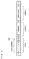
- Fig. 6 shows the original I 2 C bus protocol.
- One byte information following a start condition bit S consists of a slave address and a read/write designation bit.
- a slave address is a specific address for identifying a plurality of slave ICs connected to a bus of a single chip micro-controller which is a master.
- Command data, display data and the like are transmitted in byte units subsequent to the one byte information including a slave address, as shown in Fig. 6. Each byte must be followed by an acknowledge bit A from a slave.
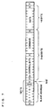
- the I 2 C bus protocol shown in Fig. 7 and Fig. 8 is developed to make it possible to send command data of one byte or more.
- a D/C bit is provided as a second high order bit of a control byte to determine which of a command or data follows.
- the I 2 C bus protocol comprises, as the multi-master-bus, all formats and procedures in a system, enabling specifications for controlling the bus by a plurality of micro-controllers as masters, for example, and hence it has high application flexibility. However, since many requirements must be fulfilled to control specific ICs, it is not always convenient to use the I 2 C bus protocol.
- the serial transmission system has the advantage that the number of terminals can be reduced to a greater extent than that of a parallel transmission system.
- this serial transmission system is inferior in speed of data transmission.
- an increase in the size of a liquid crystal screen cause liquid crystal display drivers or the like to be faced with demands for high speed data transmission.
- the outlined I 2 C bus protocol is limited in the speed-up of data transmission. This is because one byte including a slave address is required to be located at the top of each byte of a command and data, and an acknowledge bit A sent from a slave IC is always required subsequent to individual one byte information. Because the information transmitted between the master and the slave is increased in this manner, speed-up of data transmission is limited. Moreover, presence of the acknowledge bit A decreases the transfer rate of serial clock signals and restricts the speed-up of data transmission because of the following reasons.
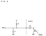
- Fig. 9 shows a signal line L of a serial data line SDA.
- a source voltage VCC is applied to the signal line L via a pull-up resistance R1 and the signal line L has its own wiring capacitance C.
- a switch SW consisting of a MOS transistor is disposed on the side of a slave IC. This switch SW is turned on to discharge the charge of the signal line L1 to thereby drop the potential to 0 V, supplying the a forementioned acknowledge bit A from the slave IC to a master micro-controller.
- a resistance R3 shown in Fig. 9 is a total resistance (such as an ITO wiring resistance and a connector resistance) from a terminal of the IC to a substrate.
- Source voltage is decreased to a lower voltage level corresponding to the miniaturization in the process.
- the on-resistance R2 of the switch SW formed by a MOS transistor for sending the acknowledge bit A of the slave IC is increased.
- the time constant for discharging the signal line L1 is thereby increased. This also hinders the speed-up of data transmission.
- the pull-up resistance R1 and the resistance (R2 + R3) divide the voltage to create a 0 level for the acknowledge bit A.
- a display driver IC which adopts a serial transmission system to reduce the number of terminal pins, transmits a command and data efficiently, and also can deal with the speed-up of data transmission and a reduction in the voltage of interface signals, and to provide an electronic device using the display driver IC.
- a display driver IC comprising:
- a serial data input signal in this case has one unit data column of (N+1) bits, which consists of one bit identification data for the identifying the command data and display data and N-bit command or display data. Accordingly, as to the number of bits of the command data and display data, N bits which are simultaneously processed by the external MPU may be allotted.
- the interface circuit may comprise:
- This structure enables data of (N+1) bits which is input serially to be subjected to serial-parallel conversion and the date to be latched onto every unit data column of (N+1) bits.
- the command decoder may generate a timing signal which is supplied for writing the display data into the storage section, on the basis of the output of the frequency dividing circuit.
- the command decoder can generate write signals on the basis of the output from the frequency dividing circuit, so that the supply of a write command from the external MPU is not required. Therefore, the load on the external MPU can be reduced and signal lines and input terminals for write signals can be omitted.
- the chip select signal may have a pulse which is non-active between continuous two unit data columns each having (N + 1) bits during an active period.
- the frequency dividing circuit and the (N +1) bit shift register may be reset by this pulse.
- Data can be latched by the (N + 1) bit latch circuit on the basis of the output from the frequency dividing circuit in this manner, thus preventing an erroneous recognition of the border between unit data columns of (N+1) bits. As a result, a data transmission error can be reduced.
- an electronic device comprising:
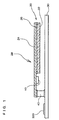
- Fig. 1 is a schematic sectional view of a display section of a portable telephone.
- the display section of the portable telephone comprises a liquid crystal module 20 with a liquid crystal display driver IC 10 mounted thereon, a print circuit board 30 with an MPU 300 mounted thereon, and a connecting section which electrically connects the liquid crystal module 20 to the print circuit board 30, specifically a rubber connecting section 40 (Zebra Rubber) which is obtained by forming a conductive section and an insulating section alternately, for example.
- the rubber connecting section has a structure in which the conductive section and the insulating section are alternately laminated, one over the other, in a direction from the rear surface to the front surface of Fig. 1.
- the terminals of the liquid crystal module 20 and the print circuit board 30 are electrically connected to each other by applying pressure uniformly in the longitudinal direction of the rubber connecting section 40.
- the liquid crystal module 20 has a liquid crystal display section 28 having a structure in which a liquid crystal 26 is sealed between two glass substrates 22 and 24.
- the liquid crystal display driver IC 10 is mounted on the extended portion of the glass substrate 24.
- the liquid crystal module 20 forms a liquid crystal display device such as a simple matrix or an active matrix.
- a segment electrode is formed on one of two glass substrates and a common electrode is formed on another glass substrate to constitute a simple matrix liquid crystal display device.
- the liquid crystal module 20 has a back light or a side light mounted thereon if it is used for a transmission type of liquid crystal display device, but requires no light source if it is a reflection type.
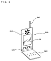
- the liquid crystal module 20 is disposed in a portable telephone 500 so that the liquid crystal display section 28 is exposed.
- the portable telephone 500 comprises a receiving section 510, a transmitting section 520, an operating section 530, an antenna 540, and the like.
- the MPU 300 sends command data or display data to the liquid crystal module 20 on the basis of the information received by the antenna 540 or the information input by the operating section 530.
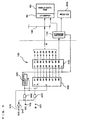
- Fig. 2 is a block diagram showing the liquid crystal display driver IC.
- the liquid crystal display driver IC 10 is provided with components for driving a liquid crystal such as a power source circuit 50, a display memory such as a display data RAM 60, a segment (SEG) driver 70 and a common (COM) driver 80 as display drivers, an oscillation circuit 90 and a display timing generation circuit 92.
- the display data RAM 60 includes memory elements equal in number (132 ⁇ 65) to pixels formed at the intersections of 132 segment electrodes SEG 0 to SEG 131 and 65 common electrodes COM 0 to COM 64.
- the liquid crystal display driver IC 10 is further provided with an MPU interface 100, a command decoder 110, and an internal bus 120.
- the MPU interface 100 has a first input terminal 101 to a fourth input terminal 104 for receiving various signals from the MPU 300.
- a serial data input signal (SI) such as command data and display data is input to the first input terminal 101
- a serial clock signal (SCL) is input to the second input terminal 102
- a chip select signal (XCS) is input to the third input terminal 103
- XRES reset signal
- command data and display data input as serial data input signals are made up of the number of bits to be processed simultaneously by the MPU 300.
- the number of bits in this embodiment is 1 byte (8 bits).
- the number of bits of command data or display data may be one word (16 bits) or one long word (32 bits).
- the MPU interface 100 receives the serial data input signal (SI) and makes a serial-parallel conversion of the serial data input signal to output the converted signal according to the serial clock signal (SCL).
- SI serial data input signal
- SCL serial clock signal
- the MPU interface 100 sends command data in parallel to the command decoder 110 if the serial data input signal (SI) is command data and sends display data in parallel to the internal bus line 120 if the serial data input signal (SI) is display data.
- the decoded command data is used as operating commands for the power source circuit 50 and the display timing generation circuit 92 and is also used in addressing by each of a page address circuit 61, a column address circuit 62, and a line address circuit 63 which are connected to the display data RAM 60.
- the parallel display data is written in memory elements according to the page and each address of the column, assigned by the command, through the internal bus 120 and an I/O buffer 64 of the display data RAM 60.
- the display data RAM 60 functions as a field or frame memory of the liquid crystal display section 28 of the liquid crystal module 20.
- the display data written in the display data RAM 60 is read out through address assignment according to a timing signal from the display timing generation circuit 92 and latched by a display data latch circuit 65.
- the display data latched by the display data latch circuit 65 is converted into data of, for instance, five potential levels V1 to V5 required for driving a liquid crystal and supplied to the segment electrodes SEG 0 to SEG 131 of the liquid crystal display section 28.
- An electric potential is supplied to the segment electrodes SEG 0 to SEG 131 based on timing signals from the display timing generation circuit 92 while switching the common electrodes COM 0 to COM 64, whereby the liquid crystal display section 28 is driven.
- Fig. 3 is a block diagram of the MPU interface 100.
- the MPU interface 100 comprises a 9 bit shift register 200, a 9 bit latch circuit 210, and a 1/9 frequency dividing circuit 220.
- the chip select signal XCS to be input through the third input terminal 103 is input to each reset terminal R of the 9 bit shift register 200 and the 1/9 frequency dividing circuit 220.
- the serial data input signal (SI) input to the first input terminal 101 is input to one input terminal of a first AND gate 240.
- the serial clock signal (SCL) input to the second input terminal 102 is input to one input terminal of a second AND gate 242.
- each logic of the serial data input signal (SI) and the serial clock signal (SCL) is output as is from the first and second AND gates 240 and 242 in the active period when the chip select signal (XCS) is LOW whereas when the chip select signal is non-active (HIGH), it is always set at LOW.
- serial data input signal SI
- serial clock signal SCL
- chip select signal XCS
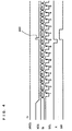
- the chip select signal (XCS) is active in LOW as shown in Fig. 4. As the chip select signal is changed from HIGH to LOW, data can be transmitted to the liquid crystal display driver IC 10.
- the chip select signal (XCS) has a pulse 400 which is changed to HIGH every 9 clock signals of the serial clock signal (SCL) in the active period.
- the serial data input signal (SI) is data using 9 bits as a unit data column.
- This unit data column is made up of a top bit D/C and data of 8 bits (1 byte).
- this identification data D/C is inserted into the top bit whereby this serial data input signal (SI) is generated.
- serial clock signal serves as a clock signal to transfer the serial data input signal (SI).
- the output X of the 1/9 frequency dividing circuit 220 is supplied to the command decoder 110.
- the output X is decoded by the command decoder 110 to thereby serve as a write signal WR for the display RAM 60 and as a clock signal which for setting a register 60A (see Fig. 3) which sets a page address in the page address circuit 61, for example.
- the reset signal XRES to be input to the fourth input terminal 104 of the MPU interface 100 is used to stop the action of the liquid crystal module 20.
- the MPU 300 makes the chip select signal (XCS) of the liquid crystal display driver IC 10 active so that an image based on the input information is displayed on the liquid crystal display section 28 and also serially sends the command data and the display data synchronously with the serial clock signal.
- XCS chip select signal
- the 1/9 frequency dividing circuit 220 of the liquid crystal display driver IC 10 divides a frequency of the serial clock signal (SCL) in 1/9 as shown in Fig. 4.
- SCL serial clock signal
- This 1/9 frequency dividing circuit 220 is reset when the chip select signal (XCS) becomes HIGH.
- the chip select signal (XCS) has a pulse 400 which is changed to HIGH after the shift register 200 takes in data D0 at a rise of the serial clock signal SCL and the latch circuit 210 latches data D0 to D9 at a rise of the output X of the 1/9 frequency dividing circuit 220.
- the 1/9 frequency dividing circuit 220 is therefore reset by the pulse 400.
- the 9 bit shift register 200 shifts sequentially the serial data input signals (SI) input to the data input terminal D at the rise of the serial clock signal (SCL) input to the clock terminal CL, and outputs these shifted signals in parallel from the output terminals Q1 to Q9.
- the output X from the 1/9 frequency dividing circuit 220 is input to the clock terminal CL of the 9 bit latch circuit 210.
- the 9 bit latch circuit 210 takes in the data from the output terminals Q1 to Q9 of the 9 bit shift register 200 at a rise (or at the ninth rise of system clock signal (SCL) shown in Fig. 4) of the pulse 400 in which the output X is changed from LOW to HIGH and latches the data until the output X becomes LOW again.
- the 8-bit data D0 to D7 is output in parallel from the terminals Q1 to Q8 of the 9 bit latch circuit 210 and the identification data D/C is output from the output terminal Q9.
- the 8-bit data D0 to D7 are input to the conunand decoder 110.
- whether or not the command decoder 110 accepts the 8-bit data D0 to D7 from the terminals Q1 to Q8 of the 9 bit latch circuit 210 is decided based on the logic of the identification data D/C. Then, the command data is decoded by the command decoder 110 and the display data is input to the I/O buffer 64.
- Command data may include high order two bits among 8-bit data assigned as the identification bits which identifies a command.
- the high order two bits are 0 and 1
- the low order 6 bits are, for example, a page address and then the address of 6 bits is set in a register.
- the output X of the 1/9 frequency dividing circuit 220 is also input to the command decoder 110 where the write signal WR shown in Fig. 4 is generated.
- the write signal WR is input to the I/O buffer 64 and used as a write timing signal for transferring the display data supplied to the I/O buffer 64 to the display data RAM 60.
- the write signal WR is also supplied to a page address register (not shown) of the page address circuit 61 and is also utilized as a clock signal for setting a page address of 6 bits in the page address register.
- the serial data input signal has a unit data column, wherein the unit is 9 bits consisting of D/C bits for the command and display data identification and one byte command or display data. Accordingly, one byte (8 bits) which is simultaneously processed by the MPU 300 may be allotted as the number of bits of the command data and display data.
- liquid crystal display driver IC 10 it is unnecessary for the liquid crystal display driver IC 10 to send the acknowledge bit A every time information of one byte is input from the MPU 300. It is therefore unnecessary to pull up a signal line connected to the first input terminal and to discharge the signal line to the LOW state every time information of one byte is input. It is hence possible to speed-up the data transmission.
- the write signal WR or the like can be generated based on the output X of the 1/9 frequency dividing circuit 220 and hence the supply of write commands from the MPU 300 is not required. Therefore, the load of MPU 300 is reduced and also signal lines and input terminals for write signals can be omitted.
- one byte (8 bits) is used for command or display data, and the number of bits of the unit data column of the serial data input signal (SI) is designed to be 9.
- the present invention is by no means limited to these bit numbers.
- the number of bits of the unit data column of the serial data input signal (SI) may be designed to be (1 + N).
- the number of bits of each of the shift register 200 and the latch circuit 210 is designed to be (1 + N)
- the frequency dividing circuit 220 is designed to divide into 1/(1 + N).
- the present invention may be applied to the case in which customers can switch from serial input to parallel input and vice versa with respect to the input of the command data, the display data and the like. This is because operations in accordance with the present invention can be implemented at least during a serial input.
- the display driver IC of the present invention is not necessarily limited to those used for liquid crystal display and may be applied to various other types of display devices.
- the electronic devices according to the present invention are not limited to portable telephones but may be applied to various other types of electronic devices which accept the input of serial data to drive liquid crystal or other display sections.
Landscapes
- Engineering & Computer Science (AREA)
- Theoretical Computer Science (AREA)
- Physics & Mathematics (AREA)
- General Physics & Mathematics (AREA)
- Human Computer Interaction (AREA)
- General Engineering & Computer Science (AREA)
- Chemical & Material Sciences (AREA)
- Crystallography & Structural Chemistry (AREA)
- Computer Hardware Design (AREA)
- Control Of Indicators Other Than Cathode Ray Tubes (AREA)
- Information Transfer Systems (AREA)
- Liquid Crystal Display Device Control (AREA)
Applications Claiming Priority (2)
| Application Number | Priority Date | Filing Date | Title |
|---|---|---|---|
| JP20896599A JP3777884B2 (ja) | 1999-07-23 | 1999-07-23 | 表示用ドライバic及びそれを用いた電子機器 |
| JP20896599 | 1999-07-23 |
Publications (2)
| Publication Number | Publication Date |
|---|---|
| EP1071067A2 true EP1071067A2 (de) | 2001-01-24 |
| EP1071067A3 EP1071067A3 (de) | 2001-10-24 |
Family
ID=16565100
Family Applications (1)
| Application Number | Title | Priority Date | Filing Date |
|---|---|---|---|
| EP00115758A Ceased EP1071067A3 (de) | 1999-07-23 | 2000-07-21 | Integrierte Treiberschaltung und elektronisches Gerät welches diese Schaltung benutzt |
Country Status (5)
| Country | Link |
|---|---|
| US (1) | US6473059B1 (de) |
| EP (1) | EP1071067A3 (de) |
| JP (1) | JP3777884B2 (de) |
| KR (1) | KR100383157B1 (de) |
| CN (1) | CN1135806C (de) |
Cited By (4)
| Publication number | Priority date | Publication date | Assignee | Title |
|---|---|---|---|---|
| EP1513059A1 (de) * | 2003-09-08 | 2005-03-09 | Barco N.V. | Pixeleinheit für Grossoberflächeanzeigevorrichtung |
| WO2006117747A1 (en) * | 2005-04-29 | 2006-11-09 | Koninklijke Philips Electronics, N.V. | 12c slave device with programmable write-transaction cycles |
| US9025454B2 (en) | 2005-12-02 | 2015-05-05 | Entegris, Inc. | I/O systems, methods and devices for interfacing a pump controller |
| CN105895005A (zh) * | 2016-06-29 | 2016-08-24 | 京东方科技集团股份有限公司 | 显示驱动芯片、显示基板、显示装置及显示驱动方法 |
Families Citing this family (10)
| Publication number | Priority date | Publication date | Assignee | Title |
|---|---|---|---|---|
| JP2002189452A (ja) * | 2000-12-19 | 2002-07-05 | Seiko Epson Corp | 半導体集積回路 |
| US7031622B2 (en) * | 2002-06-07 | 2006-04-18 | Canon Kabushiki Kaisha | Memory storing information relating to the condition of a cartridge, and image forming apparatus and cartridge having such memory |
| CN100446075C (zh) * | 2005-05-26 | 2008-12-24 | 凌阳科技股份有限公司 | 液晶面板的时序控制器与源极驱动器以及控制方法与电路 |
| CN1877995A (zh) * | 2006-01-24 | 2006-12-13 | 华为技术有限公司 | 一种芯片接口数据传送的方法和装置 |
| KR101469036B1 (ko) | 2007-02-12 | 2014-12-05 | 삼성디스플레이 주식회사 | 표시 장치 및 이를 포함하는 전자 장치 |
| TWI390405B (zh) * | 2008-12-31 | 2013-03-21 | Askey Computer Corp | 具輸出接腳擴充功能之控制裝置及輸出接腳之擴充方法 |
| JP2011133918A (ja) * | 2009-12-22 | 2011-07-07 | Meidensha Corp | リモートio子局のデータ入出力回路拡張装置 |
| KR101218543B1 (ko) * | 2010-12-30 | 2013-01-07 | 시스템베이스 주식회사 | 9-비트 시리얼 통신을 위한 제어기 |
| TWI578164B (zh) * | 2012-05-04 | 2017-04-11 | 緯創資通股份有限公司 | 資料傳輸系統、資料傳送方法以及資料接收方法 |
| KR20150057404A (ko) * | 2013-11-19 | 2015-05-28 | 삼성전자주식회사 | 디스플레이 드라이버 ic와 이를 포함하는 시스템의 동작 방법 |
Citations (2)
| Publication number | Priority date | Publication date | Assignee | Title |
|---|---|---|---|---|
| GB2271458A (en) * | 1992-07-07 | 1994-04-13 | Seiko Epson Corp | Matrix display |
| EP0740285A2 (de) | 1995-04-27 | 1996-10-30 | Canon Kabushiki Kaisha | Datenübertragungsverfahren für eine Anzeigesteuerschaltung |
Family Cites Families (7)
| Publication number | Priority date | Publication date | Assignee | Title |
|---|---|---|---|---|
| JPS60182488A (ja) * | 1984-02-29 | 1985-09-18 | 日本電気株式会社 | 駆動用電子回路 |
| DE3789743T2 (de) * | 1986-09-01 | 1994-08-18 | Nippon Electric Co | Serielles Datenübertragungssystem. |
| JP2585602B2 (ja) * | 1987-06-10 | 1997-02-26 | 株式会社日立製作所 | 半導体記憶装置 |
| US5233350A (en) * | 1991-10-21 | 1993-08-03 | Mediasonic Inc. | Apparatus and method for serial port interfacing |
| DE4230913C2 (de) * | 1992-09-16 | 1994-09-15 | Itt Ind Gmbh Deutsche | Verfahren und Schaltungsanordnung für ein serielles Bus-System mit einer Eindrahtverbindung |
| JPH0713913A (ja) | 1993-06-28 | 1995-01-17 | Sanyo Electric Co Ltd | シリアルデータ転送方法 |
| JP3661890B2 (ja) | 1995-12-15 | 2005-06-22 | ソニー株式会社 | 画像データ送信方法及び画像データ受信方法 |
-
1999
- 1999-07-23 JP JP20896599A patent/JP3777884B2/ja not_active Expired - Lifetime
-
2000
- 2000-07-19 US US09/619,471 patent/US6473059B1/en not_active Expired - Lifetime
- 2000-07-20 KR KR10-2000-0041564A patent/KR100383157B1/ko not_active Expired - Lifetime
- 2000-07-21 EP EP00115758A patent/EP1071067A3/de not_active Ceased
- 2000-07-24 CN CNB001217399A patent/CN1135806C/zh not_active Expired - Lifetime
Patent Citations (2)
| Publication number | Priority date | Publication date | Assignee | Title |
|---|---|---|---|---|
| GB2271458A (en) * | 1992-07-07 | 1994-04-13 | Seiko Epson Corp | Matrix display |
| EP0740285A2 (de) | 1995-04-27 | 1996-10-30 | Canon Kabushiki Kaisha | Datenübertragungsverfahren für eine Anzeigesteuerschaltung |
Cited By (7)
| Publication number | Priority date | Publication date | Assignee | Title |
|---|---|---|---|---|
| EP1513059A1 (de) * | 2003-09-08 | 2005-03-09 | Barco N.V. | Pixeleinheit für Grossoberflächeanzeigevorrichtung |
| US7102601B2 (en) | 2003-09-08 | 2006-09-05 | Barco, Naamloze Vennootschap | Pixel module for use in a large-area display |
| WO2006117747A1 (en) * | 2005-04-29 | 2006-11-09 | Koninklijke Philips Electronics, N.V. | 12c slave device with programmable write-transaction cycles |
| US7606956B2 (en) | 2005-04-29 | 2009-10-20 | Nxp B.V. | 12C slave device with programmable write-transaction cycles |
| US9025454B2 (en) | 2005-12-02 | 2015-05-05 | Entegris, Inc. | I/O systems, methods and devices for interfacing a pump controller |
| US9262361B2 (en) | 2005-12-02 | 2016-02-16 | Entegris, Inc. | I/O systems, methods and devices for interfacing a pump controller |
| CN105895005A (zh) * | 2016-06-29 | 2016-08-24 | 京东方科技集团股份有限公司 | 显示驱动芯片、显示基板、显示装置及显示驱动方法 |
Also Published As
| Publication number | Publication date |
|---|---|
| CN1282166A (zh) | 2001-01-31 |
| JP2001034374A (ja) | 2001-02-09 |
| EP1071067A3 (de) | 2001-10-24 |
| US6473059B1 (en) | 2002-10-29 |
| KR100383157B1 (ko) | 2003-05-12 |
| CN1135806C (zh) | 2004-01-21 |
| KR20010039730A (ko) | 2001-05-15 |
| JP3777884B2 (ja) | 2006-05-24 |
Similar Documents
| Publication | Publication Date | Title |
|---|---|---|
| US6473059B1 (en) | Display driver IC and electronic device using same | |
| EP1164570B1 (de) | Treiberschaltung mit internem ram, anzeigevorrichtung mit diesem treiber und elektronisches gerät | |
| KR101223397B1 (ko) | 데이터 처리 시스템 및 휴대 단말기 시스템 | |
| US8519926B2 (en) | Liquid crystal display device and driving method thereof | |
| US8212759B2 (en) | Control circuit and control method for LCD panel | |
| US6407730B1 (en) | Liquid crystal display device and method for transferring image data | |
| CN101354861A (zh) | 半导体集成电路设备、显示设备以及电子电路 | |
| US6130657A (en) | Liquid crystal display device | |
| CN103218985B (zh) | 传输接口与传输方法及其驱动电路与显示装置及电子装置 | |
| CN101676986A (zh) | 液晶显示器及包括液晶显示器的显示系统 | |
| CN101192397B (zh) | 用于显示控制的半导体集成电路器件 | |
| CN105679268A (zh) | 显示组件 | |
| US6232940B1 (en) | Picture data transfer control apparatus and display apparatus | |
| US11900857B2 (en) | Data transmission/reception circuit and display device including the same | |
| US7602366B2 (en) | Liquid crystal display device | |
| CN1758324A (zh) | 接口和用于显示装置的控制设备及其集成电路芯片 | |
| JP4490837B2 (ja) | 携帯端末 | |
| CN111063291A (zh) | 驱动芯片、控制板以及控制板的驱动方法 | |
| TWI745150B (zh) | 電子標籤驅動電路、多電子標籤顯示的方法以及電子標籤驅動器裝置 | |
| KR20040047442A (ko) | 액정표시장치 |
Legal Events
| Date | Code | Title | Description |
|---|---|---|---|
| PUAI | Public reference made under article 153(3) epc to a published international application that has entered the european phase |
Free format text: ORIGINAL CODE: 0009012 |
|
| AK | Designated contracting states |
Kind code of ref document: A2 Designated state(s): AT BE CH CY DE DK ES FI FR GB GR IE IT LI LU MC NL PT SE |
|
| AX | Request for extension of the european patent |
Free format text: AL;LT;LV;MK;RO;SI |
|
| PUAL | Search report despatched |
Free format text: ORIGINAL CODE: 0009013 |
|
| AK | Designated contracting states |
Kind code of ref document: A3 Designated state(s): AT BE CH CY DE DK ES FI FR GB GR IE IT LI LU MC NL PT SE |
|
| AX | Request for extension of the european patent |
Free format text: AL;LT;LV;MK;RO;SI |
|
| RIC1 | Information provided on ipc code assigned before grant |
Free format text: 7G 09G 3/20 A, 7G 09G 3/36 B, 7G 06F 3/14 B |
|
| 17P | Request for examination filed |
Effective date: 20020117 |
|
| AKX | Designation fees paid |
Free format text: AT BE CH CY DE DK ES FI FR GB GR IE IT LI LU MC NL PT SE |
|
| 17Q | First examination report despatched |
Effective date: 20080813 |
|
| STAA | Information on the status of an ep patent application or granted ep patent |
Free format text: STATUS: THE APPLICATION HAS BEEN REFUSED |
|
| 18R | Application refused |
Effective date: 20100704 |