EP1071994B1 - Dispositif memoire avec cellules memoire redondantes et procede d'acces auxdites cellules - Google Patents
Dispositif memoire avec cellules memoire redondantes et procede d'acces auxdites cellules Download PDFInfo
- Publication number
- EP1071994B1 EP1071994B1 EP99927689A EP99927689A EP1071994B1 EP 1071994 B1 EP1071994 B1 EP 1071994B1 EP 99927689 A EP99927689 A EP 99927689A EP 99927689 A EP99927689 A EP 99927689A EP 1071994 B1 EP1071994 B1 EP 1071994B1
- Authority
- EP
- European Patent Office
- Prior art keywords
- address
- block
- programmable
- column
- memory
- Prior art date
- Legal status (The legal status is an assumption and is not a legal conclusion. Google has not performed a legal analysis and makes no representation as to the accuracy of the status listed.)
- Expired - Lifetime
Links
Images

Classifications
-
- G—PHYSICS
- G06—COMPUTING OR CALCULATING; COUNTING
- G06F—ELECTRIC DIGITAL DATA PROCESSING
- G06F11/00—Error detection; Error correction; Monitoring
- G06F11/07—Responding to the occurrence of a fault, e.g. fault tolerance
- G06F11/16—Error detection or correction of the data by redundancy in hardware
- G06F11/20—Error detection or correction of the data by redundancy in hardware using active fault-masking, e.g. by switching out faulty elements or by switching in spare elements
-
- G—PHYSICS
- G11—INFORMATION STORAGE
- G11C—STATIC STORES
- G11C29/00—Checking stores for correct operation ; Subsequent repair; Testing stores during standby or offline operation
- G11C29/70—Masking faults in memories by using spares or by reconfiguring
- G11C29/78—Masking faults in memories by using spares or by reconfiguring using programmable devices
Definitions
- the invention relates to a memory arrangement with memory blocks with redundant memory cells that can be selected via addresses.
- the invention also relates to a method for accessing redundant memory cells in columns and rows in one Memory arrangement with memory blocks are arranged.
- the information to be stored is stored in individual memory cells organized into columns and rows into one Cell array are arranged, filed. Every memory cell can via column and row address lines with one assigned to them Address selected for reading or writing the cell become. For this purpose, the address lines with column and row decoders connected. These decode the address and activate the column and row address lines belonging to the address.
- the memory cells When storing larger capacity, the memory cells are in divided into several blocks. Because of the matrix-like arrangement of the memory cells, the additional cells must also be in Rows and columns are arranged. Through a programmable Element will depend on the address created selected additional lines belonging to the additional cells. These elements are programmed using so-called Fusebanks that contain laser-separable connections. When testing the memory, the addresses are found the defective memory cells are assigned. The fusebanks are then encoded in such a way that the additional addresses at these addresses (redundant) memory cells are accessed.
- EP 0 612 074 A1 describes a column redundancy circuit arrangement for a memory with several memory blocks known.
- the programmable coding elements are not assigned to the blocks there. Rather, each contains of the coding elements address decoding means and is thus one can be assigned to any memory block.
- WO 93/21578 therefore describes a memory arrangement according to the Preamble of claim 1 and a method for accessing redundant memory cells according to the preamble of claim 4 proposed, the original address of a redundancy block decoder with a pre-programmed address compared and if there is a corresponding redundancy word line decoder or redundancy bit line decoder of the corresponding memory blocks is driven to a through the redundancy word line decoder and redundancy bit line decoder access the addressed redundant memory cell, with this redundant memory cell in another Memory block as the original memory cell to be replaced can be arranged.
- the present invention has for its object a Specify memory with redundancy, where the number the defects that are rectified with redundancy lines can be increased without reducing the number of redundancy lines per block increases. This task is accomplished by a Memory arrangement with the features of claim 1 or by using a method for accessing redundant memory cells solved the features of claim 4.
- the invention has the advantage that to correct a defect the redundancy cells of a neighboring one in one memory block Memory blocks can be used. That’s it possible to fix more defects in a memory block than There are redundancy lines in this block.
- Another advantage is that both redundant for redundancy Column and redundant row lines can be used can.
- the principle according to the invention can be applied to all memory architectures (DRAM, eDRAM core, SRAM, ROM, EEPROM), which per address Write bits or more bits of information in parallel or read, be applied.
- DRAM dynamic random access memory
- eDRAM core static random access memory
- SRAM static random access memory
- ROM read-only memory
- EEPROM EEPROM
- Embodiment with the two blocks BK1 and BK2 is called that the above-mentioned defect in block BK1 with a redundant Memory cell in block BK2 can be fixed.
- a preprogrammed address is, for example, a selection address a defective memory cell of a certain block, with Redundancy memory cells of the same block cannot be fixed can, because for example all redundancy lines of this block have already been allocated for repair purposes.
- the block selection part b and the row selection part m with the preprogrammed address of the programmable Row decoder PZD2 match, so the second block BK2 activated. It is assumed that the selection address created to a defective memory cell of the first block BK1 heard.
- the line selection part m on the line decoder PZD2 is a Assigned redundancy line address part m * with which the redundancy line, which is provided for this selection address is.
- the column selection part n of the selection address is also in the Block BK2 valid.
- the defective is therefore not accessed Cell in block BK1, which is addressed with n and m, but to the redundant memory cell in block BK2, which with n and m * is addressed. So there is line redundancy.
- the row redundancy lines RZL2 of block BK2 could also be used for further any existing blocks can be used.
- the column redundancy lines SRL2 of block BK2 can be used in this Line redundancy case can only be used in the same block BK2, because otherwise more than one block would have to be activated.
- the block selection part b and the column selection part are correct e the selection address with the preprogrammed one Address of the programmable column decoder PSD2, see above the second block BK2 is activated and accordingly assigned column redundancy line SRL2 and the row selection part m a redundant memory cell in block BK2 is accessed.
- This column redundancy case is analogous to that Row redundancy case.
- With column redundancy and row redundancy in a block all redundant lines, i. H. the Row redundancy lines and the column redundancy lines, one other block provided as repair lines.
- redundancy principle can be extended to these p-blocks. Independently Any memory architecture can be implemented trace back to such a subset. Lie per block s column redundancy lines and z row redundancy lines up to p ⁇ s columns and z rows per block or s columns and p ⁇ z rows through this redundancy principle be replaced. They are usually used to fix defects the existing redundancy lines in the block itself are used. If these are not sufficient because there are several defects than can be repaired with these lines, In addition, the redundancy principle according to the invention is used.
- the existing p-blocks can be divided into two sets. For the blocks in the first set, only the column redundancy lines are used to fix defects in another Block, for the blocks of the second subset only the row redundancy lines used. It is not possible, for example the column redundancy lines of a first block to repair defects in a second block and the row redundancy lines of the first block for the repair of defects in a third block. Column redundancy lines and row redundancy lines can only be common used when both the column redundancy lines as well as the row redundancy lines both for a particular one Block can be used.
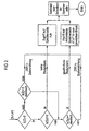
- b (Sp) 1
- a third step checks whether the column decoder for which the match was determined to the block with the block selection part b the Selection address or belongs to another block.
- the first case there is ordinary redundancy, i. H. Defective memory cells of the block BKi are made by redundancy lines of the same block BKi fixed. The block selection takes place here also via the block selection part b the selection address. It gets redundant Memory cell of the selected block accessed. Using a column redundancy line in this block takes place Access with the row selection part m and the redundancy column address part n *.
- n * specifies the column address of the one to be selected Column redundancy line.
- the defect is remedied via the line redundancy line, access to the redundant memory cell in block BKi via the column selection part n and the redundancy line address part m *.
- the query takes place as in the third step.
- Inter-block redundancy in the column direction exists if b and n with the preprogrammed address of the column decoder match and this column decoder does not match the block belongs to the block selection part b. Access to the redundant In this case, the memory cell takes place via the row selection part m and the redundancy column address part n * in the block that was previously has been assigned to the column decoder.
- the procedure for accessing the redundant memory cells can be done in parallel or sequentially.
- the method becomes the block selection part b of the selection address both to the programmable column decoders and to the programmable line decoder. Will none of the Decoder found a match, so there is no block Redundancy still inter-block redundancy. Will match one in the column decoder or row decoder Blocks, this block is used for inter-block redundancy used.
- the block selection part b is first only to either the column decoder or the row decoder directed. It is further assumed that the comparison of b and m only with the row decoders. Will not If a match is found, then b is the selection address the column decoder directed. A final selection of one Blocks is only possible if the column selection part n compared with the preprogrammed address of the column decoder becomes.
Landscapes
- Engineering & Computer Science (AREA)
- Theoretical Computer Science (AREA)
- Quality & Reliability (AREA)
- Physics & Mathematics (AREA)
- General Engineering & Computer Science (AREA)
- General Physics & Mathematics (AREA)
- For Increasing The Reliability Of Semiconductor Memories (AREA)
- Read Only Memory (AREA)
- Techniques For Improving Reliability Of Storages (AREA)
Claims (7)
- Dispositif mémoire,
avec des blocs de mémoire (BK) comportant chacun des cellules de mémoire et des cellules de mémoire redondantes qui peuvent être sélectionnées par l'intermédiaire d'adresses de sélection et qui sont disposées en colonnes et en lignes,
dans lequel il est associé aux blocs de mémoire (BK) à chaque fois au moins un décodeur de colonne programmable (PSD) et au moins un décodeur de ligne programmable (PZD) pour la sélection de l'une des cellules de mémoire redondantes dans l'un des blocs de mémoire (BK), et
dans lequel, pour au moins un bloc de mémoire (BK) déterminé, le décodeur de colonne programmable (PSD) correspondant ou le décodeur de ligne programmable (PZD) correspondant est programmé de telle sorte que le bloc de mémoire (BK) déterminé peut être sélectionné avec l'adresse de sélection pour un autre bloc de mémoire en vue d'accès à ses cellules de mémoire redondantes,
caractérisé par le fait que
le décodeur de colonne programmable (PSD) et le décodeur de ligne programmable (PZD) qui sont associés au bloc de mémoire (BK) déterminé comportent à chaque fois des moyens de comparaison pour comparer une partie fixée de l'adresse de sélection à une adresse préprogrammée, et
le décodeur de colonne programmable (PSD) et le décodeur de ligne programmable (PZD) qui sont associés au bloc de mémoire (BK) déterminé sont conçus de telle sorte que le décodeur de colonne programmable (PSD) n'effectue la comparaison entre l'adresse de sélection et l'adresse préprogrammée correspondante que si le décodeur de ligne (PZD) n'a pas trouvé de coïncidence entre l'adresse de sélection et l'adresse préprogrammée correspondante. - Dispositif mémoire selon la revendication 1,
caractérisé par le fait que
les moyens de comparaison du décodeur de colonne programmable (PSD) et du décodeur de ligne programmable (PZD) qui sont associés au bloc de mémoire (BK) déterminé sont conçus de telle sorte que, en cas de coïncidence lors de la comparaison entre l'adresse de sélection et l'adresse préprogrammée correspondante, à l'exception du bloc de mémoire (BK) déterminé, ils bloquent les autres blocs de mémoire pour des accès à des cellules de mémoire. - Dispositif mémoire selon la revendication 2,
caractérisé par le fait que
les moyens de comparaison du décodeur de colonne programmable (PSD) associé au bloc de mémoire (BK) déterminé comparent une première partie, servant à la sélection du bloc de mémoire, de l'adresse de sélection et une deuxième partie, servant à la sélection de la colonne, de l'adresse de sélection à l'adresse préprogrammée correspondante tandis que les moyens de comparaison du décodeur de ligne programmable (PZD) associé au bloc de mémoire (BK) déterminé comparent la première partie et une troisième partie, servant à la sélection de la ligne, de l'adresse de sélection à l'adresse préprogrammée correspondante. - Procédé pour l'accès à des cellules de mémoire redondantes,
dans lequel des cellules de mémoire sont disposées en colonnes et en lignes dans un dispositif mémoire comportant des blocs de mémoire (BK) auxquels sont associés à chaque fois au moins un décodeur de colonne programmable (PSD) et au moins un décodeur de ligne programmable (PZD),
dans lequel au moins une cellule de mémoire déterminée d'un bloc de mémoire (BK) déterminé est remplacée par une cellule de mémoire redondante d'un autre bloc de mémoire,
caractérisé par le fait que
la cellule de mémoire déterminée du bloc de mémoire (BK) déterminé est remplacée par la cellule de mémoire redondante de l'autre bloc de mémoire du fait qu'une adresse de sélection de la cellule de mémoire déterminée est comparée à une adresse respectivement préprogrammée de chaque décodeur de colonne programmable (PSD) et à une adresse respectivement préprogrammée de chaque décodeur de ligne programmable (PZD), et
la comparaison avec les adresses préprogrammées du décodeur de colonne (PSD) ne s'effectue que si on n'a constaté aucune coïncidence lors de la comparaison avec les adresses préprogrammées des décodeurs de ligne (PZD). - Procédé pour l'accès à des cellules de mémoire redondantes selon la revendication 4,
caractérisé par le fait que
avec une première partie de l'adresse de sélection on effectue la sélection du bloc de mémoire, avec une deuxième partie de l'adresse de sélection on effectue la sélection de la colonne et avec une troisième partie de l'adresse de sélection on effectue la sélection de la ligne de la cellule de mémoire redondante, et
on compare la première partie et la deuxième partie de l'adresse de sélection à l'adresse préprogrammée correspondante de chaque décodeur de colonne programmable (PSD) et on compare la première partie et la troisième partie de l'adresse de sélection à l'adresse préprogrammée correspondante de chaque décodeur de ligne programmable (PZD). - Procédé pour l'accès à des cellules de mémoire redondantes selon la revendication 5,
caractérisé par le fait que,
s'il y a coïncidence entre la partie correspondante de l'adresse de sélection et l'une des adresses préprogrammées, on libère l'accès aux cellules de mémoire redondantes du bloc de mémoire dont le décodeur de colonne ou de ligne associé (PSD ; PZD) donne la coïncidence. - Procédé pour l'accès à des cellules de mémoire redondantes selon la revendication 6,
caractérisé par le fait que
on associe une nouvelle adresse à la deuxième partie ou à la troisième partie ou à la deuxième partie et à la troisième partie de l'adresse de sélection en vue de l'accès à la cellule de mémoire redondante.
Applications Claiming Priority (3)
| Application Number | Priority Date | Filing Date | Title |
|---|---|---|---|
| DE19817159 | 1998-04-17 | ||
| DE19817159 | 1998-04-17 | ||
| PCT/DE1999/001181 WO1999054819A1 (fr) | 1998-04-17 | 1999-04-16 | Dispositif memoire avec cellules memoire redondantes et procede d'acces auxdites cellules |
Publications (2)
| Publication Number | Publication Date |
|---|---|
| EP1071994A1 EP1071994A1 (fr) | 2001-01-31 |
| EP1071994B1 true EP1071994B1 (fr) | 2002-10-30 |
Family
ID=7864902
Family Applications (1)
| Application Number | Title | Priority Date | Filing Date |
|---|---|---|---|
| EP99927689A Expired - Lifetime EP1071994B1 (fr) | 1998-04-17 | 1999-04-16 | Dispositif memoire avec cellules memoire redondantes et procede d'acces auxdites cellules |
Country Status (7)
| Country | Link |
|---|---|
| US (1) | US6466493B1 (fr) |
| EP (1) | EP1071994B1 (fr) |
| JP (1) | JP2002512416A (fr) |
| KR (1) | KR100621265B1 (fr) |
| DE (1) | DE59903253D1 (fr) |
| TW (1) | TW582041B (fr) |
| WO (1) | WO1999054819A1 (fr) |
Families Citing this family (6)
| Publication number | Priority date | Publication date | Assignee | Title |
|---|---|---|---|---|
| US6144593A (en) * | 1999-09-01 | 2000-11-07 | Micron Technology, Inc. | Circuit and method for a multiplexed redundancy scheme in a memory device |
| KR100351902B1 (ko) * | 2000-09-28 | 2002-09-12 | 주식회사 하이닉스반도체 | 칼럼 리던던시 리페어 회로 |
| DE10155449A1 (de) * | 2001-11-12 | 2003-05-28 | Infineon Technologies Ag | Verfahren zur Rekonfiguration eines Speichers |
| US6868019B2 (en) * | 2003-07-02 | 2005-03-15 | Micron Technology, Inc. | Reduced power redundancy address decoder and comparison circuit |
| JP4607685B2 (ja) | 2005-06-30 | 2011-01-05 | 富士通セミコンダクター株式会社 | 半導体メモリ |
| US20080266990A1 (en) * | 2007-04-30 | 2008-10-30 | Infineon Technologies North America Corp. | Flexible redundancy replacement scheme for semiconductor device |
Family Cites Families (13)
| Publication number | Priority date | Publication date | Assignee | Title |
|---|---|---|---|---|
| US4051354A (en) * | 1975-07-03 | 1977-09-27 | Texas Instruments Incorporated | Fault-tolerant cell addressable array |
| US4937790A (en) * | 1987-08-31 | 1990-06-26 | Hitachi, Ltd. | Semiconductor memory device |
| US4807191A (en) * | 1988-01-04 | 1989-02-21 | Motorola, Inc. | Redundancy for a block-architecture memory |
| US5270975A (en) * | 1990-03-29 | 1993-12-14 | Texas Instruments Incorporated | Memory device having a non-uniform redundancy decoder arrangement |
| US5257229A (en) * | 1992-01-31 | 1993-10-26 | Sgs-Thomson Microelectronics, Inc. | Column redundancy architecture for a read/write memory |
| JP3040625B2 (ja) * | 1992-02-07 | 2000-05-15 | 松下電器産業株式会社 | 半導体記憶装置 |
| DE59205881D1 (de) * | 1992-04-16 | 1996-05-02 | Siemens Ag | Integrierter halbleiterspeicher mit redundanzeinrichtung |
| EP0612074B1 (fr) | 1993-02-19 | 2001-05-02 | Infineon Technologies AG | Dispositif de colonnes redondantes pour une mémoire |
| US5404331A (en) * | 1993-07-30 | 1995-04-04 | Sgs-Thomson Microelectronics, Inc. | Redundancy element check in IC memory without programming substitution of redundant elements |
| JPH08180698A (ja) * | 1994-12-22 | 1996-07-12 | Toshiba Corp | 半導体記憶装置 |
| KR0145222B1 (ko) * | 1995-05-20 | 1998-08-17 | 김광호 | 반도체 메모리장치의 메모리 셀 테스트 제어회로 및 방법 |
| KR0170271B1 (ko) * | 1995-12-30 | 1999-03-30 | 김광호 | 리던던트셀 테스트 제어회로를 구비하는 반도체 메모리장치 |
| US5970000A (en) * | 1998-02-02 | 1999-10-19 | International Business Machines Corporation | Repairable semiconductor integrated circuit memory by selective assignment of groups of redundancy elements to domains |
-
1999
- 1999-04-16 EP EP99927689A patent/EP1071994B1/fr not_active Expired - Lifetime
- 1999-04-16 TW TW088106115A patent/TW582041B/zh not_active IP Right Cessation
- 1999-04-16 JP JP2000545099A patent/JP2002512416A/ja active Pending
- 1999-04-16 KR KR1020007011482A patent/KR100621265B1/ko not_active Expired - Fee Related
- 1999-04-16 WO PCT/DE1999/001181 patent/WO1999054819A1/fr not_active Ceased
- 1999-04-16 DE DE59903253T patent/DE59903253D1/de not_active Expired - Fee Related
-
2000
- 2000-10-17 US US09/690,298 patent/US6466493B1/en not_active Expired - Lifetime
Also Published As
| Publication number | Publication date |
|---|---|
| TW582041B (en) | 2004-04-01 |
| JP2002512416A (ja) | 2002-04-23 |
| KR20010042751A (ko) | 2001-05-25 |
| DE59903253D1 (de) | 2002-12-05 |
| KR100621265B1 (ko) | 2006-09-13 |
| US6466493B1 (en) | 2002-10-15 |
| WO1999054819A1 (fr) | 1999-10-28 |
| EP1071994A1 (fr) | 2001-01-31 |
Similar Documents
| Publication | Publication Date | Title |
|---|---|---|
| DE69019697T2 (de) | Reparierbare Speicherschaltung. | |
| DE3032630C2 (de) | Halbleiterspeicher aus Speicherbausteinen mit redundanten Speicherbereichen und Verfahren zu dessen Betrieb | |
| DE60110297T2 (de) | Speichervorrichtung mit elektrisch programmierbaren Sicherungen | |
| EP1046993B1 (fr) | Circuit de mémoire à auto-test incorporé | |
| DE69411532T2 (de) | Verfahren zur Programmierung von Redundanzregistern in einer Zeilenredundanzschaltung für einen Halbleiterspeicherbaustein | |
| DE10110469A1 (de) | Integrierter Speicher und Verfahren zum Testen und Reparieren desselben | |
| DE69907997T2 (de) | Halbleiterspeicherschaltung mit Redundanz | |
| EP1444699A1 (fr) | Procede de reconfiguration d'une memoire | |
| EP1008993B1 (fr) | Mémoire avec dispositif de auto-test et sa mèthode | |
| DE69911364T2 (de) | Verfahren und Vorrichtung zur Parallelredundanz bei Halbleiterspeichern | |
| DE69906406T2 (de) | Reparierbare integrierte Halbleiterspeicherschaltung mit selektiver Zuweisung von Redundanzgruppen zu Domänen | |
| DE60011035T2 (de) | Verfahren zur logischen Aufteilung einer nichtflüchtigen Speichermatrix | |
| DE19963689A1 (de) | Schaltungsanordnung eines integrierten Halbleiterspeichers zum Speichern von Adressen fehlerhafter Speicherzellen | |
| DE10229802B3 (de) | Testschaltung und Verfahren zum Testen einer integrierten Speicherschaltung | |
| EP1055238B1 (fr) | Circuit et procede pour controler un circuit numerique a semi-conducteur | |
| DE69100796T2 (de) | Integrierte Speicherschaltung mit Redundanz und verbesserter Adressierung in Testbetriebsart. | |
| DE69323076T2 (de) | Verfahren zur Erkennung fehlerhafter Elemente eines redundanten Halbleiterspeichers | |
| DE19830362A1 (de) | Halbleiterspeichervorrichtung | |
| DE4201847C2 (de) | Halbleiterspeicherbauelement mit einem redundanten Zellenfeld | |
| EP1071994A1 (fr) | Dispositif memoire avec cellules memoire redondantes et procede d'acces auxdites cellules | |
| DE10331068A1 (de) | Verfahren zum Auslesen von Fehlerinformationen aus einem integrierten Baustein und integrierter Speicherbaustein | |
| DE19924153B4 (de) | Schaltungsanordnung zur Reparatur eines Halbleiterspeichers | |
| DE10229164A1 (de) | Speicherbaustein mit einem Datengenerator und einer Testlogik und Verfahren zum Testen von Speicherzellen eines Speicherbausteins | |
| DE102007013316A1 (de) | Mehrbanklesen und Datenkomprimierung für Ausgangstests | |
| DE10139724A1 (de) | Integrierter Speicher mit Speicherzellen in mehreren Speicherzellenblöcken und Verfahren zum Betrieb eines solchen Speichers |
Legal Events
| Date | Code | Title | Description |
|---|---|---|---|
| PUAI | Public reference made under article 153(3) epc to a published international application that has entered the european phase |
Free format text: ORIGINAL CODE: 0009012 |
|
| 17P | Request for examination filed |
Effective date: 20001009 |
|
| AK | Designated contracting states |
Kind code of ref document: A1 Designated state(s): DE FR GB IE IT |
|
| GRAG | Despatch of communication of intention to grant |
Free format text: ORIGINAL CODE: EPIDOS AGRA |
|
| GRAG | Despatch of communication of intention to grant |
Free format text: ORIGINAL CODE: EPIDOS AGRA |
|
| 17Q | First examination report despatched |
Effective date: 20011009 |
|
| GRAG | Despatch of communication of intention to grant |
Free format text: ORIGINAL CODE: EPIDOS AGRA |
|
| GRAG | Despatch of communication of intention to grant |
Free format text: ORIGINAL CODE: EPIDOS AGRA |
|
| GRAH | Despatch of communication of intention to grant a patent |
Free format text: ORIGINAL CODE: EPIDOS IGRA |
|
| GRAH | Despatch of communication of intention to grant a patent |
Free format text: ORIGINAL CODE: EPIDOS IGRA |
|
| GRAA | (expected) grant |
Free format text: ORIGINAL CODE: 0009210 |
|
| AK | Designated contracting states |
Kind code of ref document: B1 Designated state(s): DE FR GB IE IT |
|
| REG | Reference to a national code |
Ref country code: GB Ref legal event code: FG4D Free format text: NOT ENGLISH |
|
| REG | Reference to a national code |
Ref country code: IE Ref legal event code: FG4D Free format text: GERMAN |
|
| REF | Corresponds to: |
Ref document number: 59903253 Country of ref document: DE Date of ref document: 20021205 |
|
| GBT | Gb: translation of ep patent filed (gb section 77(6)(a)/1977) |
Effective date: 20030127 |
|
| ET | Fr: translation filed | ||
| PLBE | No opposition filed within time limit |
Free format text: ORIGINAL CODE: 0009261 |
|
| STAA | Information on the status of an ep patent application or granted ep patent |
Free format text: STATUS: NO OPPOSITION FILED WITHIN TIME LIMIT |
|
| 26N | No opposition filed |
Effective date: 20030731 |
|
| PGFP | Annual fee paid to national office [announced via postgrant information from national office to epo] |
Ref country code: GB Payment date: 20070426 Year of fee payment: 9 |
|
| PGFP | Annual fee paid to national office [announced via postgrant information from national office to epo] |
Ref country code: DE Payment date: 20080613 Year of fee payment: 10 |
|
| PGFP | Annual fee paid to national office [announced via postgrant information from national office to epo] |
Ref country code: IT Payment date: 20080424 Year of fee payment: 10 |
|
| PGFP | Annual fee paid to national office [announced via postgrant information from national office to epo] |
Ref country code: IE Payment date: 20080424 Year of fee payment: 10 |
|
| PGFP | Annual fee paid to national office [announced via postgrant information from national office to epo] |
Ref country code: FR Payment date: 20080412 Year of fee payment: 10 |
|
| GBPC | Gb: european patent ceased through non-payment of renewal fee |
Effective date: 20080416 |
|
| PG25 | Lapsed in a contracting state [announced via postgrant information from national office to epo] |
Ref country code: GB Free format text: LAPSE BECAUSE OF NON-PAYMENT OF DUE FEES Effective date: 20080416 |
|
| REG | Reference to a national code |
Ref country code: FR Ref legal event code: ST Effective date: 20091231 |
|
| PG25 | Lapsed in a contracting state [announced via postgrant information from national office to epo] |
Ref country code: DE Free format text: LAPSE BECAUSE OF NON-PAYMENT OF DUE FEES Effective date: 20091103 |
|
| REG | Reference to a national code |
Ref country code: IE Ref legal event code: MM4A |
|
| PG25 | Lapsed in a contracting state [announced via postgrant information from national office to epo] |
Ref country code: IE Free format text: LAPSE BECAUSE OF NON-PAYMENT OF DUE FEES Effective date: 20090416 Ref country code: FR Free format text: LAPSE BECAUSE OF NON-PAYMENT OF DUE FEES Effective date: 20091222 |
|
| PG25 | Lapsed in a contracting state [announced via postgrant information from national office to epo] |
Ref country code: IT Free format text: LAPSE BECAUSE OF NON-PAYMENT OF DUE FEES Effective date: 20090416 |