EP1073192A2 - Dispositif de contrôle d'une charge à courant alternatif , en particulier d'un moteur à courant alternatif avec contrôle de vitesse - Google Patents
Dispositif de contrôle d'une charge à courant alternatif , en particulier d'un moteur à courant alternatif avec contrôle de vitesse Download PDFInfo
- Publication number
- EP1073192A2 EP1073192A2 EP00114987A EP00114987A EP1073192A2 EP 1073192 A2 EP1073192 A2 EP 1073192A2 EP 00114987 A EP00114987 A EP 00114987A EP 00114987 A EP00114987 A EP 00114987A EP 1073192 A2 EP1073192 A2 EP 1073192A2
- Authority
- EP
- European Patent Office
- Prior art keywords
- voltage
- load
- current
- input
- switching elements
- Prior art date
- Legal status (The legal status is an assumption and is not a legal conclusion. Google has not performed a legal analysis and makes no representation as to the accuracy of the status listed.)
- Granted
Links
Images




Classifications
-
- H—ELECTRICITY
- H02—GENERATION; CONVERSION OR DISTRIBUTION OF ELECTRIC POWER
- H02M—APPARATUS FOR CONVERSION BETWEEN AC AND AC, BETWEEN AC AND DC, OR BETWEEN DC AND DC, AND FOR USE WITH MAINS OR SIMILAR POWER SUPPLY SYSTEMS; CONVERSION OF DC OR AC INPUT POWER INTO SURGE OUTPUT POWER; CONTROL OR REGULATION THEREOF
- H02M7/00—Conversion of AC power input into DC power output; Conversion of DC power input into AC power output
- H02M7/42—Conversion of DC power input into AC power output without possibility of reversal
- H02M7/44—Conversion of DC power input into AC power output without possibility of reversal by static converters
- H02M7/48—Conversion of DC power input into AC power output without possibility of reversal by static converters using discharge tubes with control electrode or semiconductor devices with control electrode
- H02M7/53—Conversion of DC power input into AC power output without possibility of reversal by static converters using discharge tubes with control electrode or semiconductor devices with control electrode using devices of a triode or transistor type requiring continuous application of a control signal
- H02M7/537—Conversion of DC power input into AC power output without possibility of reversal by static converters using discharge tubes with control electrode or semiconductor devices with control electrode using devices of a triode or transistor type requiring continuous application of a control signal using semiconductor devices only, e.g. single switched pulse inverters
- H02M7/5387—Conversion of DC power input into AC power output without possibility of reversal by static converters using discharge tubes with control electrode or semiconductor devices with control electrode using devices of a triode or transistor type requiring continuous application of a control signal using semiconductor devices only, e.g. single switched pulse inverters in a bridge configuration
-
- H—ELECTRICITY
- H02—GENERATION; CONVERSION OR DISTRIBUTION OF ELECTRIC POWER
- H02P—CONTROL OR REGULATION OF ELECTRIC MOTORS, ELECTRIC GENERATORS OR DYNAMO-ELECTRIC CONVERTERS; CONTROLLING TRANSFORMERS, REACTORS OR CHOKE COILS
- H02P27/00—Arrangements or methods for the control of AC motors characterised by the kind of supply voltage
- H02P27/04—Arrangements or methods for the control of AC motors characterised by the kind of supply voltage using variable-frequency supply voltage, e.g. inverter or converter supply voltage
- H02P27/06—Arrangements or methods for the control of AC motors characterised by the kind of supply voltage using variable-frequency supply voltage, e.g. inverter or converter supply voltage using DC to AC converters or inverters
- H02P27/08—Arrangements or methods for the control of AC motors characterised by the kind of supply voltage using variable-frequency supply voltage, e.g. inverter or converter supply voltage using DC to AC converters or inverters with pulse width modulation
Definitions
- the present invention relates to a system for operation an AC load, especially an AC motor, whereby an input AC voltage to a pulsating, input DC voltage consisting of sine half-waves rectified and from this DC input voltage via a power amplifier with controlled, in one Bridge circuit arranged electronic switching elements a clocked, pulse-width-modulated load AC voltage is generated by in the range of Zero crossings of the AC input voltage the switching elements the commutation stage.
- the invention is therefore based on the object a system of the generic type from the described prior art Way of creating the operating behavior is further improved.
- reduced noise can be achieved.
- this is achieved in that one from the Load AC voltage resulting load current for determination a possible phase shift relative to the voltage is monitored, and that in the event of a detected Phase shift each time the input AC voltage and the load current of different polarities have, the output stage is controlled in such a way that a timing of the AC load and a sinusoidal curve of the Load current result.
- the invention is thus based on the knowledge that the problems described at the outset occur in the prior art when there is a phase shift between the load voltage and the load current. This is the case with a motor in most operating points because of the motor winding acting as an inductive load; the load current then lags the load voltage. If the voltage has its zero crossing and consequently the switching elements are commutated, the load current is not yet zero.
- monitoring is therefore initially carried out automatically on possible phase shift, and if the phase shift is detected, the critical times with different polarities of voltage and electricity a special novel control of the Switching elements of the output stage in such a way that then also in these Areas a continuous clocking of the load AC voltage is achieved.
- This advantageously results at least with an inductive or capacitive load an optimal sinusoidal curve of the load current. From the The sine curve of the current then results in every working point an optimally low operating noise.
- a generic - and in principle also a system according to the invention - has an output stage 2 with four semiconductor switching elements (transistors) T3, T4, T5 and T6 connected in a full bridge, preferably by FETs (MOSFET) or IGBT's are formed.
- a load L to be operated is located in the middle transverse bridge branch of the full bridge, ie at circuit points A and B.
- an intermediate circuit capacitor C Z In parallel with the bridge circuit is an intermediate circuit capacitor C Z , the capacitance of which is so small that the voltage form of the rectified sine half-waves is not significantly changed.
- this capacitor C Z It is the task of this capacitor C Z to absorb the energy supplied by the motor in the phases of different voltage and current polarities, since it is not possible for the rectifier to feed back into the network.
- this capacitor can be designed as a robust film capacitor instead of an electrolytic capacitor.
- each switching element T3 to T6 Parallel to the switching path (drain-source) of each switching element T3 to T6 is a free-wheeling diode D3 to D6.
- the output stage 2 is preceded by a (bridge) rectifier circuit 4, which rectifies an input AC voltage U N (for example mains voltage) to a pulsating, unsmoothed input DC voltage U E, which thus consists of half-sine waves.
- the switching elements T3 to T6 of the output stage are then controlled in pairs by a control unit 6 (cf. also FIGS. 5, 20 and 21) in such a way that a load alternating voltage U L by reversing the polarity essentially from the to supply the load L.
- Half waves of the input DC voltage U E is composed.
- this load alternating voltage U L for setting the power is clocked in a pulse-width-modulated manner by one (T3 or T5) of the two electronic switching elements of each pair T3, T6 or T4, T5 can be pulse-width-modulated with a constant clock frequency, in particular above human hearing, while the other switching element (T6 or T4) of the respective pair is switched through completely.
- Another type of control whereby T6 or T4 are clocked and T3 or T5 are controlled, is equivalent.
- the load alternating voltage U L is clocked at a constant frequency but with a variable pulse width. 2 was recorded with a reduced clock frequency for reasons of illustration. In practice, however, as already mentioned, the clock frequency is above the audible range, that is above about 16 kHz and in particular about 20 kHz.
- the amplitude of the resulting load current i L can be changed by means of a variable pulse / pause ratio (so-called PWM modulation). In the event that the load L is a motor, this results in a change in the speed (slip control). In times when the load alternating voltage u L is zero due to the clock, it is ensured that the load current i L can still flow in the same direction. This is done by the freewheeling diode D4 and the controlled transistor T6 or by D6 and T4.
- the present invention comes in, according to which the load current i L is first automatically monitored for a phase shift relative to the load AC voltage u L or to the relevant phase position of the input AC voltage U N. If a phase shift is determined as a result, the output stage 2 is controlled by the control unit 6 in a new, special way in the areas of unequal polarity of voltage and current in such a way that a clocking of the voltage and an optimally sinusoidal load current is achieved in this area become.
- the areas 1 and 3 are the normal operating times t B , in which the output stage 2 is actuated unchanged in a known manner - as already briefly described above.
- the areas 2 and 4 are so-called commutation times t KOM , in which a special new control according to the invention is provided.
- the control according to the invention of the individual switching elements of the output stage 2 in the different areas of a period is shown in the following table: transistor 1. Same polarity positive half wave 2. different polarity pos. Half wave 3. Same polarity negative half wave 4. Different polarity neg.
- Half wave T3 clocked blocked blocked blocked blocked T4 blocked blocked controlled clocked T5 blocked blocked blocked clocked blocked T6 controlled clocked blocked blocked blocked
- T6 is constant in area 1.
- T6 is controlled while T3 with a variable pulse / pause ratio is clocked.
- area 3 T4 controlled and T5 clocked accordingly.
- the load current is now in the 2nd and 4th ranges the times when the voltage is zero for clocking should be redirected to a free-running branch. This happens, by only one switching element T4 or T6 is clocked while all other switching elements are locked are.
- the respective clocked Switching element T4 or T6 with a - compared to the "normal" Impulse / pause ratio in the areas 1. and 3. - inverted pulse / pause ratio controlled.
- Areas 1 and 3 each have the input voltage the load when the clocked switching element switches through, and when it locks, the voltage is zero. In the fields of 2. and 4. this is exactly the opposite according to the invention.
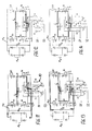
- 11 and 12 illustrate the first area of the period with T6 controlled and T3 clocked (T4, T5 blocked).
- the clocked T3 is just conductive.
- the clocked T3 is currently locked.
- the current then continues to flow via a voltage-free freewheeling branch via the load L, the conductive T6 and the freewheeling diode D4 of the blocked T4.
- the voltage is zero.
- 13 and 14 show the second area of the period with the control according to the invention of only T6 clocked in an inverted manner (T3, T4, T5 blocked).
- T3, T4, T5 blocked the current flows from C Z via D4, L, D5 to C z , so that the voltage corresponds to the curve U N (t) (circuit via C Z ).
- the voltage becomes zero, the current continuing to flow in accordance with its sine curve via the freewheeling branch L, T6, D4.
- the third area of the period is illustrated in FIGS. 15 and 16, T5 being clocked and T4 being controlled (T3, T6 blocked). 15, the clocked T5 is just conductive, so that the current flows through T5, L and T4 and the voltage is U N (t). 16, when the clocked T5 is blocked, the current flows again via a freewheeling circuit L, T4 and D6, so that the voltage is zero.
- FIGS. 17 and 18 wherein according to the invention only T4 is clocked inverted (T3, T5, T6 blocked). 17, when T4 is currently blocked, the current flows back through a circuit from C Z via D6, L and D3 to C Z ; the voltage corresponds to U N (t). According to FIG. 18, the voltage becomes zero in that T4 is switched through in a clocked manner and the current flows via the freewheeling circuit L, T4, D6.
- FIG. 10 a possible circuit is shown in FIG. 10.
- two diodes D1 and D2 are connected in series to a supply voltage U V , the connection point Q of which is connected to the AC input voltage U N via a high-resistance resistor R.
- the supply voltage U V is, for example, + 5V.
- the diodes D1 and D2 cut off everything from the sinusoidal AC input voltage U N that is ⁇ 5.7V and ⁇ -0.7V. In times when the voltage value of the input AC voltage is - 0.7V ⁇ U N ⁇ 5.7V, the same potential is present at point Q corresponding to the voltage U N.
- point Q is either constant -0.7V or constant 5.7V.
- approximately a square wave signal is generated, which has the value 5.7V during the positive half-wave of the input AC voltage and -0.7V during the negative half-wave.
- the diode circuit 12 preferably consists of four diodes D11, D21, D31 and D41, in pairs (D11, D41; D21, D31) are connected antiparallel, the point between the is grounded (minus the rectifier circuit 4).
- the respective forward voltages are preferably two transistors Controlled T1 and / or T2, the control signals S1 and S2 generate over the current state. These control signals S1 and S2 are also fed to the control unit 6.
- the (NPN) transistor T1 is connected with its emitter at point C, its base via resistor R1 at point D. Accordingly, the (NPN) transistor T2 is connected with its emitter at point D, its base via resistor R2 am Point C.
- the collectors are each connected via a resistor R3 or R4 to a supply voltage U B of, for example, 5V.
- the positive Half wave of the load current are considered (Fig. 11 to 14).
- the current flows on his already described above 11 also via D21.
- D21 and D41 are in series in the current path.
- the current also flows in series via D21 and D41.
- T6 is locked (Fig. 13)
- D41 is in the current path.
- the load current lags behind the load voltage.
- the zero crossing of the load current then takes place at the end of the positive half-wave in the "different polarity" range.
- the current flow through the corresponding diodes D21 and / or D41 also stops.
- the potential difference between point C and D decreases, which blocks T1, since its base is no longer at least 0.7V more positive than the emitter.
- the control signal S1 now jumps to high (approx. + U B ) due to the blocking transistor T1.
- 11 to 14 show all possible current paths during the positive half wave of the current. Regardless of the operating state in which the zero crossing of the load current occurs, the control signal S1 always jumps immediately from low to high.
- a signal S1 is thus generated by this circuit, which at the end of the positive half wave at the zero crossing the load current jumps from low to high. During the For the entire negative half-wave, this signal S1 is high. Only jumps after the beginning of the next positive half wave it back to low.
- the transistor T2 with the diodes D11 and / or D31 cooperates and the control signal S2 generated, which during the negative halves low and is high during the positive half wave.
- This preferred circuit can advantageously be used the zero crossing of the load current is then reliably recognized if the load L behaves capacitively (current rushes voltage), because at least one of the diodes is always on is flowed through by the current.
- control unit 6 can clearly delimit the four working areas described per period from one another and control the above table.
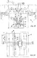
- a capacitor C34 and C29 is provided here in parallel with each half of the bridge circuit (T3, T4 and T5, T6). Since the line inductances prevent the motor current from being immediately taken over by C Z , without these capacitors C29 and C34, overvoltage would occur during commutation due to excessive di / dt, which could destroy electronic components.
- the capacitors C29 and C34 are arranged directly on the respective transistor half bridge in order to keep the line inductances small.
- the associated control unit 6 has a microcontroller ⁇ C, the inputs of which usually contain a protective circuit comprising two diodes. They can possibly be used as part of the voltage detection 8 according to FIG. 10, so that externally only the resistor R (here, for example, as a series connection of two resistors R51 and R52) has to be provided for connection to the AC input voltage U N.
- a microcontroller ⁇ C the inputs of which usually contain a protective circuit comprising two diodes. They can possibly be used as part of the voltage detection 8 according to FIG. 10, so that externally only the resistor R (here, for example, as a series connection of two resistors R51 and R52) has to be provided for connection to the AC input voltage U N.
- control unit 6 is here made up of logic gates.
- the one from these gates built circuit can also be in monolithic or hybrid integrated form (e.g. ASIC; FPGA; PAL etc).
- control unit is 6 5 with a device 14 for setting connected to the engine speed.
- This speed controller 14 can for example have the structure according to FIG. 20 or FIG. 21.
- the invention is not based on the illustrated and described Embodiments limited, but also includes all designs having the same effect in the sense of the invention. Furthermore, the invention is not yet based on the Claim 1 defined combination of features limited, but can also be by any other combination of certain characteristics of all of the individual characteristics disclosed be defined. This means that basically practically every single feature of claim 1 omitted or by at least one elsewhere in the registration disclosed individual feature can be replaced. To that extent claim 1 only as a first attempt at formulation to understand for an invention.
Landscapes
- Engineering & Computer Science (AREA)
- Power Engineering (AREA)
- Inverter Devices (AREA)
- Control Of Ac Motors In General (AREA)
Applications Claiming Priority (2)
| Application Number | Priority Date | Filing Date | Title |
|---|---|---|---|
| DE19935048A DE19935048A1 (de) | 1999-07-26 | 1999-07-26 | System zum Betreiben einer Wechselstromlast, insbesondere eines Wechselstrom-Motors mit Drehzahleinstellung |
| DE19935048 | 1999-07-26 |
Publications (3)
| Publication Number | Publication Date |
|---|---|
| EP1073192A2 true EP1073192A2 (fr) | 2001-01-31 |
| EP1073192A3 EP1073192A3 (fr) | 2003-05-02 |
| EP1073192B1 EP1073192B1 (fr) | 2005-01-12 |
Family
ID=7916103
Family Applications (1)
| Application Number | Title | Priority Date | Filing Date |
|---|---|---|---|
| EP00114987A Expired - Lifetime EP1073192B1 (fr) | 1999-07-26 | 2000-07-20 | Procédé et dispositif de contrôle d'une charge à courant alternatif , en particulier d'un moteur à courant alternatif avec contrôle de vitesse |
Country Status (3)
| Country | Link |
|---|---|
| EP (1) | EP1073192B1 (fr) |
| AT (1) | ATE287138T1 (fr) |
| DE (2) | DE19935048A1 (fr) |
Cited By (15)
| Publication number | Priority date | Publication date | Assignee | Title |
|---|---|---|---|---|
| US7190597B2 (en) | 2004-06-17 | 2007-03-13 | Vacon Oyj | Control of an inverter pulse-width modulator |
| US9645584B2 (en) | 2014-09-17 | 2017-05-09 | Honeywell International Inc. | Gas valve with electronic health monitoring |
| US9657946B2 (en) | 2012-09-15 | 2017-05-23 | Honeywell International Inc. | Burner control system |
| US9683674B2 (en) | 2013-10-29 | 2017-06-20 | Honeywell Technologies Sarl | Regulating device |
| US9835265B2 (en) | 2011-12-15 | 2017-12-05 | Honeywell International Inc. | Valve with actuator diagnostics |
| US9841122B2 (en) | 2014-09-09 | 2017-12-12 | Honeywell International Inc. | Gas valve with electronic valve proving system |
| US9846440B2 (en) | 2011-12-15 | 2017-12-19 | Honeywell International Inc. | Valve controller configured to estimate fuel comsumption |
| US9851103B2 (en) | 2011-12-15 | 2017-12-26 | Honeywell International Inc. | Gas valve with overpressure diagnostics |
| US10422531B2 (en) | 2012-09-15 | 2019-09-24 | Honeywell International Inc. | System and approach for controlling a combustion chamber |
| US10503181B2 (en) | 2016-01-13 | 2019-12-10 | Honeywell International Inc. | Pressure regulator |
| US10564062B2 (en) | 2016-10-19 | 2020-02-18 | Honeywell International Inc. | Human-machine interface for gas valve |
| US10697632B2 (en) | 2011-12-15 | 2020-06-30 | Honeywell International Inc. | Gas valve with communication link |
| US10697815B2 (en) | 2018-06-09 | 2020-06-30 | Honeywell International Inc. | System and methods for mitigating condensation in a sensor module |
| US11073281B2 (en) | 2017-12-29 | 2021-07-27 | Honeywell International Inc. | Closed-loop programming and control of a combustion appliance |
| CN115360939A (zh) * | 2022-09-26 | 2022-11-18 | 浙江特康电子科技有限公司 | 一种电机控制装置及其方法 |
Families Citing this family (10)
| Publication number | Priority date | Publication date | Assignee | Title |
|---|---|---|---|---|
| DE102004062580B4 (de) * | 2004-08-23 | 2008-07-24 | Diehl Ako Stiftung & Co. Kg | Verfahren und Vorrichtung zur Regelung eines mehrphasigen, elektronisch kommutierten Motors |
| EP1816739B1 (fr) | 2006-02-04 | 2008-04-09 | Diehl AKO Stiftung & Co. KG | Procédé et dispositif de contrôle d'un moteur polyphasée et à commutation électronique |
| DE102009005702A1 (de) | 2008-01-29 | 2009-07-30 | Ebm-Papst St. Georgen Gmbh & Co. Kg | Elektronisch kommutierter Motor |
| US8899264B2 (en) | 2011-12-15 | 2014-12-02 | Honeywell International Inc. | Gas valve with electronic proof of closure system |
| US9074770B2 (en) | 2011-12-15 | 2015-07-07 | Honeywell International Inc. | Gas valve with electronic valve proving system |
| US8947242B2 (en) | 2011-12-15 | 2015-02-03 | Honeywell International Inc. | Gas valve with valve leakage test |
| US8839815B2 (en) | 2011-12-15 | 2014-09-23 | Honeywell International Inc. | Gas valve with electronic cycle counter |
| US8905063B2 (en) | 2011-12-15 | 2014-12-09 | Honeywell International Inc. | Gas valve with fuel rate monitor |
| US9995486B2 (en) | 2011-12-15 | 2018-06-12 | Honeywell International Inc. | Gas valve with high/low gas pressure detection |
| US10024439B2 (en) | 2013-12-16 | 2018-07-17 | Honeywell International Inc. | Valve over-travel mechanism |
Family Cites Families (6)
| Publication number | Priority date | Publication date | Assignee | Title |
|---|---|---|---|---|
| DE3539647C2 (de) * | 1985-11-08 | 1994-05-26 | Asea Brown Boveri | Schaltungsanordnung für einen pulsgesteuerten Wechselstromsteller |
| DE3841147A1 (de) * | 1988-12-07 | 1990-06-13 | Mulfingen Elektrobau Ebm | Verfahren zum ansteuern eines wechselstrom-motors sowie nach diesem verfahren ansteuerbarer wechselstrom-motor |
| DE4428682C2 (de) * | 1994-08-12 | 1997-01-23 | Robert Seuffer Gmbh & Co | Verfahren zur Versorgung einer induktiven Last mit sinusförmigem Wechselstrom und Wechselstromsteller hierfür |
| US5627447A (en) * | 1995-09-29 | 1997-05-06 | Allen-Bradley Company, Inc. | Method and apparatus for detecting current delay angle from motor terminal voltage |
| DE19612117A1 (de) * | 1996-03-27 | 1997-10-02 | Telefunken Microelectron | Vorrichtung zum Erzeugen einer netzsynchronen Versorgungsspannung für Wechselstromverbraucher |
| DE19831159B4 (de) * | 1998-07-11 | 2004-06-03 | Carl Freudenberg Kg | Drehzahladaptiver Schwingungstilger |
-
1999
- 1999-07-26 DE DE19935048A patent/DE19935048A1/de not_active Withdrawn
-
2000
- 2000-07-20 AT AT00114987T patent/ATE287138T1/de not_active IP Right Cessation
- 2000-07-20 DE DE50009194T patent/DE50009194D1/de not_active Expired - Lifetime
- 2000-07-20 EP EP00114987A patent/EP1073192B1/fr not_active Expired - Lifetime
Cited By (18)
| Publication number | Priority date | Publication date | Assignee | Title |
|---|---|---|---|---|
| US7190597B2 (en) | 2004-06-17 | 2007-03-13 | Vacon Oyj | Control of an inverter pulse-width modulator |
| US10697632B2 (en) | 2011-12-15 | 2020-06-30 | Honeywell International Inc. | Gas valve with communication link |
| US10851993B2 (en) | 2011-12-15 | 2020-12-01 | Honeywell International Inc. | Gas valve with overpressure diagnostics |
| US9851103B2 (en) | 2011-12-15 | 2017-12-26 | Honeywell International Inc. | Gas valve with overpressure diagnostics |
| US9835265B2 (en) | 2011-12-15 | 2017-12-05 | Honeywell International Inc. | Valve with actuator diagnostics |
| US9846440B2 (en) | 2011-12-15 | 2017-12-19 | Honeywell International Inc. | Valve controller configured to estimate fuel comsumption |
| US9657946B2 (en) | 2012-09-15 | 2017-05-23 | Honeywell International Inc. | Burner control system |
| US10422531B2 (en) | 2012-09-15 | 2019-09-24 | Honeywell International Inc. | System and approach for controlling a combustion chamber |
| US11421875B2 (en) | 2012-09-15 | 2022-08-23 | Honeywell International Inc. | Burner control system |
| US9683674B2 (en) | 2013-10-29 | 2017-06-20 | Honeywell Technologies Sarl | Regulating device |
| US9841122B2 (en) | 2014-09-09 | 2017-12-12 | Honeywell International Inc. | Gas valve with electronic valve proving system |
| US10203049B2 (en) | 2014-09-17 | 2019-02-12 | Honeywell International Inc. | Gas valve with electronic health monitoring |
| US9645584B2 (en) | 2014-09-17 | 2017-05-09 | Honeywell International Inc. | Gas valve with electronic health monitoring |
| US10503181B2 (en) | 2016-01-13 | 2019-12-10 | Honeywell International Inc. | Pressure regulator |
| US10564062B2 (en) | 2016-10-19 | 2020-02-18 | Honeywell International Inc. | Human-machine interface for gas valve |
| US11073281B2 (en) | 2017-12-29 | 2021-07-27 | Honeywell International Inc. | Closed-loop programming and control of a combustion appliance |
| US10697815B2 (en) | 2018-06-09 | 2020-06-30 | Honeywell International Inc. | System and methods for mitigating condensation in a sensor module |
| CN115360939A (zh) * | 2022-09-26 | 2022-11-18 | 浙江特康电子科技有限公司 | 一种电机控制装置及其方法 |
Also Published As
| Publication number | Publication date |
|---|---|
| ATE287138T1 (de) | 2005-01-15 |
| EP1073192A3 (fr) | 2003-05-02 |
| DE19935048A1 (de) | 2001-02-08 |
| EP1073192B1 (fr) | 2005-01-12 |
| DE50009194D1 (de) | 2005-02-17 |
Similar Documents
| Publication | Publication Date | Title |
|---|---|---|
| EP1073192B1 (fr) | Procédé et dispositif de contrôle d'une charge à courant alternatif , en particulier d'un moteur à courant alternatif avec contrôle de vitesse | |
| DE69506612T2 (de) | Steuerschaltung für induktive Belastung | |
| EP2297842B1 (fr) | Procédé, agencement de commutation et circuit en pont | |
| EP1520331B1 (fr) | Procede et ensemble circuit pour limiter une surtension | |
| DE69937203T2 (de) | Stromwandlervorrichtung | |
| EP2193597B1 (fr) | Hacheur multi-canaux fonctionnant à la limite de la discontinuité indépendamment de la puissance de sortie | |
| DE102014103454A1 (de) | System und Verfahren für einen Schaltleistungswandler | |
| DE19741655A1 (de) | Schaltung zur stufenlosen direkten oder indirekten Variation des durch einen von einer Netz-Gleich- oder -Wechselspannung oder einer beliebigen Kombination derselben betriebenen Verbraucher fließenden Gleich- und/oder Wechselstroms | |
| DE102007040550A1 (de) | Steuerungsschema für einen Gleichstrom/Wechselstrom-Direktumrichter | |
| EP2116857A1 (fr) | Procédé et dispositif de détermination d'une polarité de courant à l'intérieur d'une branche de pont cadençée | |
| DE3841147C2 (fr) | ||
| DE102020201810B4 (de) | Stromrichter-Schaltung | |
| DE10156939A1 (de) | Schaltungsanordnung zum Betreiben einer elektrischenMaschine | |
| EP0024300A1 (fr) | Procédé pour le contrôle de la durée d'impulsion d'un régulateur inverseur à courant continu et circuit pour la mise en oeuvre dudit procédé | |
| DE69206503T2 (de) | Hochgeschwindigkeits-gleichstrommotor. | |
| DE69838358T2 (de) | Elektronisch kommutierter Motor | |
| DE2930907A1 (de) | Verfahren zur pulsbreitensteuerung eines gleichstrom-umkehrstellers und schaltungsanordnung zur durchfuehrung des verfahrens | |
| DE2900338C2 (fr) | ||
| DE19910327C2 (de) | Verfahren zum Betrieb eines Drehstromumrichters für Drehstrommotoren | |
| DE19711768B4 (de) | Elektromagnetischer Stellantrieb | |
| AT390532B (de) | Pulsbreiten moduliertes wechselstrom-leistungsstellglied | |
| WO2016012465A1 (fr) | Circuit pour onduleur multipoints npc comprenant un réseau de décharge | |
| DE102006060828A1 (de) | Umrichter mit einer Verzögerungsschaltung für PWM-Signale | |
| DE3539647C2 (de) | Schaltungsanordnung für einen pulsgesteuerten Wechselstromsteller | |
| DE102005045552B4 (de) | Schaltungsanordnung |
Legal Events
| Date | Code | Title | Description |
|---|---|---|---|
| PUAI | Public reference made under article 153(3) epc to a published international application that has entered the european phase |
Free format text: ORIGINAL CODE: 0009012 |
|
| AK | Designated contracting states |
Kind code of ref document: A2 Designated state(s): AT BE CH CY DE DK ES FI FR GB GR IE IT LI LU MC NL PT SE |
|
| AX | Request for extension of the european patent |
Free format text: AL;LT;LV;MK;RO;SI |
|
| PUAL | Search report despatched |
Free format text: ORIGINAL CODE: 0009013 |
|
| AK | Designated contracting states |
Designated state(s): AT BE CH CY DE DK ES FI FR GB GR IE IT LI LU MC NL PT SE |
|
| AX | Request for extension of the european patent |
Extension state: AL LT LV MK RO SI |
|
| 17P | Request for examination filed |
Effective date: 20030503 |
|
| 17Q | First examination report despatched |
Effective date: 20031111 |
|
| AKX | Designation fees paid |
Designated state(s): AT BE CH CY DE DK ES FI FR GB GR IE IT LI LU MC NL PT SE |
|
| RAP1 | Party data changed (applicant data changed or rights of an application transferred) |
Owner name: EBM-PAPST MULFINGEN GMBH & CO.KG |
|
| GRAP | Despatch of communication of intention to grant a patent |
Free format text: ORIGINAL CODE: EPIDOSNIGR1 |
|
| RTI1 | Title (correction) |
Free format text: METHOD AND DEVICE FOR DRIVING AN AC LOAD, ESPECIALLY AN AC MOTOR WITH SPEED CONTROL |
|
| GRAS | Grant fee paid |
Free format text: ORIGINAL CODE: EPIDOSNIGR3 |
|
| GRAA | (expected) grant |
Free format text: ORIGINAL CODE: 0009210 |
|
| AK | Designated contracting states |
Kind code of ref document: B1 Designated state(s): AT BE CH CY DE DK ES FI FR GB GR IE IT LI LU MC NL PT SE |
|
| PG25 | Lapsed in a contracting state [announced via postgrant information from national office to epo] |
Ref country code: FI Free format text: LAPSE BECAUSE OF FAILURE TO SUBMIT A TRANSLATION OF THE DESCRIPTION OR TO PAY THE FEE WITHIN THE PRESCRIBED TIME-LIMIT Effective date: 20050112 Ref country code: IE Free format text: LAPSE BECAUSE OF FAILURE TO SUBMIT A TRANSLATION OF THE DESCRIPTION OR TO PAY THE FEE WITHIN THE PRESCRIBED TIME-LIMIT Effective date: 20050112 Ref country code: NL Free format text: LAPSE BECAUSE OF FAILURE TO SUBMIT A TRANSLATION OF THE DESCRIPTION OR TO PAY THE FEE WITHIN THE PRESCRIBED TIME-LIMIT Effective date: 20050112 |
|
| REG | Reference to a national code |
Ref country code: GB Ref legal event code: FG4D Free format text: NOT ENGLISH |
|
| REG | Reference to a national code |
Ref country code: CH Ref legal event code: EP Ref country code: CH Ref legal event code: NV Representative=s name: TROESCH SCHEIDEGGER WERNER AG |
|
| REF | Corresponds to: |
Ref document number: 50009194 Country of ref document: DE Date of ref document: 20050217 Kind code of ref document: P |
|
| REG | Reference to a national code |
Ref country code: IE Ref legal event code: FG4D Free format text: GERMAN |
|
| GBT | Gb: translation of ep patent filed (gb section 77(6)(a)/1977) |
Effective date: 20050222 |
|
| PG25 | Lapsed in a contracting state [announced via postgrant information from national office to epo] |
Ref country code: DK Free format text: LAPSE BECAUSE OF FAILURE TO SUBMIT A TRANSLATION OF THE DESCRIPTION OR TO PAY THE FEE WITHIN THE PRESCRIBED TIME-LIMIT Effective date: 20050412 |
|
| REG | Reference to a national code |
Ref country code: SE Ref legal event code: TRGR |
|
| PG25 | Lapsed in a contracting state [announced via postgrant information from national office to epo] |
Ref country code: ES Free format text: LAPSE BECAUSE OF FAILURE TO SUBMIT A TRANSLATION OF THE DESCRIPTION OR TO PAY THE FEE WITHIN THE PRESCRIBED TIME-LIMIT Effective date: 20050423 |
|
| NLV1 | Nl: lapsed or annulled due to failure to fulfill the requirements of art. 29p and 29m of the patents act | ||
| PG25 | Lapsed in a contracting state [announced via postgrant information from national office to epo] |
Ref country code: LU Free format text: LAPSE BECAUSE OF NON-PAYMENT OF DUE FEES Effective date: 20050720 Ref country code: AT Free format text: LAPSE BECAUSE OF NON-PAYMENT OF DUE FEES Effective date: 20050720 Ref country code: CY Free format text: LAPSE BECAUSE OF FAILURE TO SUBMIT A TRANSLATION OF THE DESCRIPTION OR TO PAY THE FEE WITHIN THE PRESCRIBED TIME-LIMIT Effective date: 20050720 |
|
| PG25 | Lapsed in a contracting state [announced via postgrant information from national office to epo] |
Ref country code: MC Free format text: LAPSE BECAUSE OF NON-PAYMENT OF DUE FEES Effective date: 20050731 Ref country code: BE Free format text: LAPSE BECAUSE OF NON-PAYMENT OF DUE FEES Effective date: 20050731 |
|
| REG | Reference to a national code |
Ref country code: IE Ref legal event code: FD4D |
|
| ET | Fr: translation filed | ||
| PLBE | No opposition filed within time limit |
Free format text: ORIGINAL CODE: 0009261 |
|
| STAA | Information on the status of an ep patent application or granted ep patent |
Free format text: STATUS: NO OPPOSITION FILED WITHIN TIME LIMIT |
|
| 26N | No opposition filed |
Effective date: 20051013 |
|
| BERE | Be: lapsed |
Owner name: EBM-PAPST MULFINGEN G.M.B.H. & CO.KG Effective date: 20050731 |
|
| PG25 | Lapsed in a contracting state [announced via postgrant information from national office to epo] |
Ref country code: PT Free format text: LAPSE BECAUSE OF NON-PAYMENT OF DUE FEES Effective date: 20050612 |
|
| PG25 | Lapsed in a contracting state [announced via postgrant information from national office to epo] |
Ref country code: GR Free format text: LAPSE BECAUSE OF NON-PAYMENT OF DUE FEES Effective date: 20050112 |
|
| PGFP | Annual fee paid to national office [announced via postgrant information from national office to epo] |
Ref country code: CH Payment date: 20100824 Year of fee payment: 11 |
|
| PGFP | Annual fee paid to national office [announced via postgrant information from national office to epo] |
Ref country code: SE Payment date: 20100719 Year of fee payment: 11 Ref country code: DE Payment date: 20100923 Year of fee payment: 11 Ref country code: FR Payment date: 20100722 Year of fee payment: 11 |
|
| PGFP | Annual fee paid to national office [announced via postgrant information from national office to epo] |
Ref country code: GB Payment date: 20100714 Year of fee payment: 11 |
|
| PG25 | Lapsed in a contracting state [announced via postgrant information from national office to epo] |
Ref country code: IT Free format text: LAPSE BECAUSE OF NON-PAYMENT OF DUE FEES Effective date: 20100720 |
|
| PGFP | Annual fee paid to national office [announced via postgrant information from national office to epo] |
Ref country code: IT Payment date: 20100722 Year of fee payment: 11 |
|
| PGRI | Patent reinstated in contracting state [announced from national office to epo] |
Ref country code: IT Effective date: 20110616 |
|
| REG | Reference to a national code |
Ref country code: CH Ref legal event code: PL |
|
| REG | Reference to a national code |
Ref country code: SE Ref legal event code: EUG |
|
| GBPC | Gb: european patent ceased through non-payment of renewal fee |
Effective date: 20110720 |
|
| REG | Reference to a national code |
Ref country code: FR Ref legal event code: ST Effective date: 20120330 |
|
| PG25 | Lapsed in a contracting state [announced via postgrant information from national office to epo] |
Ref country code: LI Free format text: LAPSE BECAUSE OF NON-PAYMENT OF DUE FEES Effective date: 20110731 Ref country code: CH Free format text: LAPSE BECAUSE OF NON-PAYMENT OF DUE FEES Effective date: 20110731 Ref country code: FR Free format text: LAPSE BECAUSE OF NON-PAYMENT OF DUE FEES Effective date: 20110801 Ref country code: DE Free format text: LAPSE BECAUSE OF NON-PAYMENT OF DUE FEES Effective date: 20120201 |
|
| REG | Reference to a national code |
Ref country code: DE Ref legal event code: R119 Ref document number: 50009194 Country of ref document: DE Effective date: 20120201 |
|
| PG25 | Lapsed in a contracting state [announced via postgrant information from national office to epo] |
Ref country code: IT Free format text: LAPSE BECAUSE OF NON-PAYMENT OF DUE FEES Effective date: 20110720 |
|
| PG25 | Lapsed in a contracting state [announced via postgrant information from national office to epo] |
Ref country code: GB Free format text: LAPSE BECAUSE OF NON-PAYMENT OF DUE FEES Effective date: 20110720 |
|
| PG25 | Lapsed in a contracting state [announced via postgrant information from national office to epo] |
Ref country code: SE Free format text: LAPSE BECAUSE OF NON-PAYMENT OF DUE FEES Effective date: 20110721 |