EP1073203B1 - Steuerschaltung für einen Pegelumsetzer-Hochspannungsschalter - Google Patents
Steuerschaltung für einen Pegelumsetzer-Hochspannungsschalter Download PDFInfo
- Publication number
- EP1073203B1 EP1073203B1 EP00402167A EP00402167A EP1073203B1 EP 1073203 B1 EP1073203 B1 EP 1073203B1 EP 00402167 A EP00402167 A EP 00402167A EP 00402167 A EP00402167 A EP 00402167A EP 1073203 B1 EP1073203 B1 EP 1073203B1
- Authority
- EP
- European Patent Office
- Prior art keywords
- transistor
- transistors
- circuit
- voltage input
- voltage
- Prior art date
- Legal status (The legal status is an assumption and is not a legal conclusion. Google has not performed a legal analysis and makes no representation as to the accuracy of the status listed.)
- Expired - Lifetime
Links
- 230000015654 memory Effects 0.000 claims description 17
- 230000010287 polarization Effects 0.000 description 8
- 230000006870 function Effects 0.000 description 4
- 235000021183 entrée Nutrition 0.000 description 3
- 239000002784 hot electron Substances 0.000 description 3
- 230000000694 effects Effects 0.000 description 2
- 238000005516 engineering process Methods 0.000 description 2
- 238000000034 method Methods 0.000 description 2
- 230000001419 dependent effect Effects 0.000 description 1
- 238000001514 detection method Methods 0.000 description 1
- 238000012905 input function Methods 0.000 description 1
- 238000012163 sequencing technique Methods 0.000 description 1
- 230000001052 transient effect Effects 0.000 description 1
Images


Classifications
-
- H—ELECTRICITY
- H03—ELECTRONIC CIRCUITRY
- H03K—PULSE TECHNIQUE
- H03K17/00—Electronic switching or gating, i.e. not by contact-making and –breaking
- H03K17/10—Modifications for increasing the maximum permissible switched voltage
- H03K17/102—Modifications for increasing the maximum permissible switched voltage in field-effect transistor switches
-
- H—ELECTRICITY
- H03—ELECTRONIC CIRCUITRY
- H03K—PULSE TECHNIQUE
- H03K3/00—Circuits for generating electric pulses; Monostable, bistable or multistable circuits
- H03K3/02—Generators characterised by the type of circuit or by the means used for producing pulses
- H03K3/353—Generators characterised by the type of circuit or by the means used for producing pulses by the use, as active elements, of field-effect transistors with internal or external positive feedback
- H03K3/356—Bistable circuits
- H03K3/356104—Bistable circuits using complementary field-effect transistors
- H03K3/356113—Bistable circuits using complementary field-effect transistors using additional transistors in the input circuit
Definitions
- the present invention relates to a device for control of a high voltage switch type translator.
- An application example concerns circuits integrated with volatile none memories electrically programmable.
- a high voltage switch also called levels.
- This switch receives, as inputs, a logic signal and a high voltage input.
- Vcc or 0 of the logic control signal which in the case of a memory will come from a signal of write command, we get at the output of switch, either ground or input level high tension.
- CMOS switches In the invention, we are more interested particularly CMOS switches. They understand usually two branches, with in each branch two transistors in series between the high voltage input and mass. The bottom transistors are of type N and have their sources connected to ground. They are also called switching transistors, because these are them who receive one the switching signal, and the other the reverse switching signal. These signals switching signals are logic signals whose level is 0 or Vcc.
- the top transistors are P type and have their sources connected to a node receiving the high input voltage. They each have their grid connected to the drain from the top transistor of the other branch. They are also called charge transistors.
- the operating principle is as follows: depending on the levels of the switching signals there are always a switching transistor N which is blocked, the switching N transistor of the other branch being passing. This passing transistor N draws its drain towards 0 volt (the potential of its source), and the transistor P of the other branch which has its grid connected to this drain becomes a passer-by: it therefore brings its own drain to the voltage from its source, namely at the input high tension.
- These switches usually include a intermediate stage, between the stage of the transistors of the top and the bottom of the transistors.
- This floor intermediate comprises one or more cascode stages. It allows to limit voltage levels intermediary the internal nodes of the switch, so that no switch transistor sees a too high voltage across its terminals.
- all MOS transistors (N or P) of the cascode stage are polarized on their grid by the voltage Vcc logic supply. This polarization limits the switch operating range. The tilt the switch to get the level of the high voltage input can only be done when the entry level is high enough, in practice higher than the supply voltage Vcc logic.
- the gates of these cascode transistors are then usually biased at a reference voltage V REF not greater than a reference voltage V REF p which polarizes the gate of the P type transistors of the cascode stage. This lowers the lower switch limit of the switch.
- FIG. 1 An example of a cascode stage switch of this type is shown in figure 1.
- the upper stage comprises in the first branch, a P type transistor M, M1, and in the second branch, a P type transistor M, M2. These transistors receive at their source, the high voltage input E HV .
- the bottom stage comprises an N-type Mos transistor, M3, and in the second branch, an N-type Mos transistor, M4. These transistors have their source connected to ground G ND .
- the cascode stage comprises four Mos transistors: two P-type Mos transistors, M5 and M6, one in each branch, under each top transistor and two N-type Mos transistors, M7 and M8, one in each branch, above of each bottom transistor.
- the MOS P M5 and M6 transistors receive the reference voltage V REF p on their grid.
- the MOS N transistors M7 and M8 receive the reference voltage V REF not on their grid.
- the VOUT output of the switch is taken between the N and P cascode transistors of a branch, with drains transistors M6 and M8 in the example.
- the gate of the bottom transistor M3 of the first branch of the switch receives a switching logic signal denoted IN, and the gate of the bottom transistor M4 of the second branch of the switch receives the reverse signal, denoted / I N.
- the REF circuit for generating reference voltages V REF not and V REF p comprises three Mos transistors M9, M10, M11 in series between the high voltage V PP and the ground. These three transistors operate in resistance since they each have their gate connected to their drain. In the example, they are of type P.
- the reference voltages V REF not and V REF p are obtained by taking the voltage on either side of the middle transistor and M10.
- the role of the cascode stage is to limit to intermediate levels the tensions seen by transistors.
- Each P-type cascode transistor is polarized so as to always remain on. Thus its source, and therefore, the drain of the charge transistor P to which it is connected, cannot drop below V REF p - Vt p , where Vt p is the threshold voltage of the type P cascode transistor.
- each N-type cascode transistor is polarized so as to always remain on. Thus its source, and therefore, the drain of the switching transistor N to which it is connected, cannot rise above V REF not - Vt n , where Vt n is the threshold voltage of the type N cascode transistor.
- the two curves 2 and 3 represent the evolution of the reference voltage, V REF not , V REF p .
- An object of the invention is to solve this problem technical.
- the idea behind the invention is to make switch the switch to low values of the high voltage input. Once the transistors have switched, the high voltage input level may mount, without risk for these transistors.
- This switching in the low values of the high voltage input is carried out by means of a control circuit controlled by a binary control signal.
- this control circuit makes it possible to impose as bias voltages of the gates of the cascode transistors, either the logic supply voltage Vcc and the ground, or the reference voltages V REF not , V REF p state of the art.
- the levels of the logic supply voltages Vcc and G ND ) can be forced as bias voltages of the cascode transistors, to make the switch switch to low voltage.
- the switch can still switch in the high values of the high voltage input.
- the invention therefore makes it possible to widen the range of operation of the switch to low values high voltage input, improve its reliability and to simplify its drawing rules.
- the invention therefore relates to a device for controlling a switch of a high voltage input, with MOS transistors and comprising at least one cascode stage, the device comprising a circuit for generating reference voltages from the high voltage input. and outputting one or more bias voltages of the transistors Mos of the cascode stage, characterized in that it further comprises a control circuit of the reference generation circuit, controlled by a binary signal, for either forcing the voltages of polarization at the level of the logic supply voltages Vcc and G ND , allowing the switching of the switch even in low values of the high voltage input, ie allowing the establishment of the polarization voltages by the reference generation circuit.
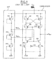
- FIG. 3 represents a device for controlling a switch of a high voltage input E HV according to the invention.
- the control device comprises a REF circuit for generating the reference voltages and a COM control circuit.
- the REF circuit includes, as in the state of the art, three P-type Mos transistors M12, M13 and M14, connected in series between the node N, receiving the high voltage input E HV , and the ground G ND . But only the first and the third transistors M12 and M14 each have their gate connected to their drain.
- the second transistor M13 is controlled by a control circuit COM according to the invention. Its drain and its source respectively provide a first bias voltage V POL 1 and a second bias voltage V POL 2 . These are the gate bias voltages of the transistors of the cascode stage (s).
- the COM control circuit makes it possible to control the grid, drain and source voltage of the second transistor M13, depending on the level of a control signal / WR.
- An integrated circuit CI in this example comprises a electrically programmable non-volatile memory plan, noted MEM.
- Access to memory is controlled by a decoder DEC based on address and control signals (not shown).
- the decoder output signals are signals logical.
- a circuit 10 of high voltage switches 11 is placed for this purpose between the decoder and the memory.
- the IN command input of each switch is provided by one of the decoder output signals.
- These switches receive a high voltage input E HV supplied by a high voltage multiplexer circuit 20. They receive the bias voltages of the cascode transistors of the control device 30 according to the invention.
- the multiplexer circuit 20 receives as inputs the logic supply voltage Vcc and a high voltage V PP , in the example supplied by a high voltage generator HVGEN (charge pump).
- HVGEN charge pump
- This write signal / WR is also applied to the control device 30 which supplies the voltages of polarization of the cascode transistors to the switches.
- the signals IN, E HV , V OUT are represented in figure 4 and the signals / WR, V POL 1 V POL 2 and E HV are shown in Figure 5.
- the multiplexer 20 applies Vcc to the high voltage input E HV and the decoder is activated to output as selection signals function of address signals (ADR) applied as input.
- this input IN flip-flop When this input IN flip-flop from 0 to 1, for switching on the output node V OUT of the switch, the level of the high voltage HV E input, this input E HV is still at a level less than or equal to Vcc.
- V POL 1 and V POL 2 are then forced by the control device 30 to the levels of the logic supply voltages, that is to say respectively Vcc (2 volts in the example) and G ND .
- the multiplexer 20 applies the programming voltage to the high voltage input E HV in the form of a pulse, with a ramp up in voltage from the previous level Vcc, to V PP .
- the polarization voltages V POL 1 and V POL 2 then follow the rise of the high voltage input E HV , as shown in FIG. 5.
- the output signal V OUT also follows the high voltage input E HV .
- the switch well ensures its functionality of keeping the output information during the rise of the high voltage input E HV .
- V REF signals not and V REF p visible in FIG. 5 are linked to the switching of the switch (capacitive effect of the MOS transistors M5 to M8).
- the control device according to the invention therefore makes it possible to widen the operating range of the switch by enabling it to switch not only in the high values, as in the prior art, but also in the low values (E HV ⁇ VDC).
- the invention applies to programming elements as well of a memory plan, only to the programming of elements discrete memories, distributed in different circuits internal of an integrated circuit. This may include electrically programmable fuses used in redundancy or other circuits.
- Figure 3 shows an exemplary embodiment detailed view of a control circuit according to the invention.
- This control circuit mainly comprises four Mos transistors M15, M16, M17 and M18.
- the P-type transistor M15 is connected between the logic supply voltage Vcc and the first intermediate node A of the reference circuit REF, connected to the source of transistor M13.
- the N-type transistor M16 is connected between the second intermediate node B of the reference circuit, connected to the drain of the transistor M13, and the ground G ND .
- the P-type Mos transistor M17 is connected between the logic supply voltage Vcc and the gate of the transistor M13.
- the transistor M18 is connected between the gate of the second transistor and the second intermediate node B, connected to the drain of transistor M13.
- the transistors M16 and M18 are controlled on their gate by the control signal / WR of the control circuit and the transistor M15 is controlled by a signal VNP referenced at the high voltage input E HV and coming from the signal / WR and of reverse logic .
- the transistor M17 is connected on its gate to the second intermediate node B.
- the transistor M18 is blocked. Also, the transistor M17, which is on, brings the voltage Vcc on the gate of transistor M13, which is thus forced in the blocked state.
- the transistor M15 is also passing, since the signal VNP is of reverse logic to signal / WR. he therefore brings the voltage Vcc to the first node intermediate A.
- the intermediate nodes A and B are reinforced in their respective levels Vcc and G ND , whatever the voltage level on l 'high voltage input.
- the transistors M15 and M16 go to the blocked state, and consequently the transistor M17 also goes into the off state.
- the transistor M18 turns on and actively connects the gate of the transistor M13 to the second intermediate node B, that is to say to its drain.
- the transistor M13 is then found connected as a diode like the other transistors M12 and M14 of the reference circuit. We find the normal operation of the reference circuit: the voltages at nodes A and B follow the rise in voltage of the high voltage input E HV .
- the transistor M15 of the control circuit is connected between the logic supply voltage Vcc and the node A and that the transistor M12 of the reference circuit is connected between the high voltage input E HV and the node A, when this input high voltage E HV reaches the high values, it must be certain that the transistor M15 is properly blocked, so as not to send high voltage to the logic supply voltage Vcc.
- the transistor M15 must receive on its gate not the high level corresponding to the logic supply voltage Vcc, but that from the high voltage input E HV .
- V PP the nominal value
- a first P-type Mos transistor, M19, a second N-type Mos transistor, M20 and a third N-type Mos transistor M21 are connected in series between the node N the high voltage input E HV and the ground G ND .
- the transistor M21 is controlled on its gate by the control signal / WR.
- Transistors M20 and M19 have their gates linked together at the first intermediate node A.
- the reverse logic signal V NP and referenced to E HV by the inverter is supplied by the serial connection point between the two transistors M19 and M20. It is the signal applied to the gate of transistor M15.
- the sizes of the MOS transistors 19, 20 and 21 are dimensioned so that, even if the high voltage input E HV takes a value greater than Vcc, V NP remains less than Vcc - V tp , so that the switch operates even in the high values of the high voltage input (i.e. it can switch).
- V NP V PP , M15 blocked and V REF not less than V PP -V tp .
- the bulks of the transistors M15, M17, M19 and M12 are polarized by the high voltage input E HV .
- the bulks of the transistors M18 and M12 are polarized by the voltage at the first intermediate node A, for better voltage withstand.
- the invention which has just been described allows improve operating range and reliability high voltage switches, allowing its switching at low values of the high input voltage. Its practical realization is a little expensive, since it includes, in the exemplary embodiment described, seven additional transistors.
- the input E HV does not necessarily have the form with two bearings Vcc, V PP shown in FIG. 4.
- the invention is not limited to the examples of embodiment and application described. It extends to control devices comprising a control circuit capable of forcing the voltage levels Vcc and G ND as bias voltages of the cascode transistors of the switch into low voltage values of the signal E HV .
- the invention applies in general to MOS switches with one or more cascade stages using one or both bias voltages, depending on whether these cascade stages are with N and P MOS transistors, with transistors MOS N or MOS P transistors.
Landscapes
- Logic Circuits (AREA)
- Read Only Memory (AREA)
Claims (10)
- Steuerschaltung für einen Wandler eines Hochspannungseingangs (EHV) mit MOS-Transistoren und wenigstens einer Kaskadenstufe, wobei die Schaltung einen Generatorschaltkreis (REF) für das Erzeugen von Referenzspannungen (VREFN, VREFP) aus dem Hochspannungseingang (EHV) und das Erzeugen am Ausgang einer oder mehrerer Vorspannungen (VPOL1, VPOL2) für MOS-Transistoren der Kaskadenstufe umfasst, dadurch gekennzeichnet, dass sie außerdem einen Steuerschaltkreis (COM) für den Referenzgeneratorschaltkreis (REF) umfasst, der gesteuert wird durch ein Binärsignal (/WR), um entweder die Vorspannungen auf den Pegel von den logischen Versorgungsspannungen VCC und GND (VPOL1 = VCC, VPOL2 = GND) zu zwingen, wodurch der Wandler selbst bei niedrigen Werten an dem Hochspannungseingang (EHV) wandelt, oder um das Aufbauen von Vorspannungen durch den Referenzgeneratorschaltkreis zu ermöglichen (VPOL1 = VREFn, VPOL2 = VREFp).
- Steuerschaltung nach Anspruch 1, wobei der Referenzgeneratorschaltkreis (REF) einen PMOS-Transistor (M12), der zwischen einen Knoten (N), der mit dem Hochspannungseingang (EHV) verbunden ist, und einen ersten Zwischenknoten (A) geschaltet ist und dessen Gate mit seinem Drain verbunden ist, einen zweiten PMOS-Transistor (M13), der zwischen den ersten Zwischenknoten (A) und einen zweiten Zwischenknoten (B) geschaltet ist, und einen dritten PMOS-Transistor (M14) umfasst, der zwischen den zweiten Knoten und Masse geschaltet ist und dessen Gate mit seinem Drain verbunden ist, wobei sich eine Vorspannung (VPOL1, VPOL2) an dem einen oder anderen der Zwischenknoten ergibt, dadurch gekennzeichnet, dass der Steuerschaltkreis Steuervorrichtungen für den zweiten Transistor (M13) umfasst, um entweder den ersten und den zweiten Zwischenknoten (A, B) auf die Pegel der logischen Versorgungsspannungen (VCC, GND) zu zwingen, oder aktiv das Gate und den Drain des zweiten Transistors (M13) zu verbinden, wodurch das Aufbauen von Spannungspegeln an dem ersten und dem zweiten Zwischenknoten durch den Referenzgeneratorschaltkreis (REF) ermöglicht wird.
- Steuerschaltung nach Anspruch 2, dadurch gekennzeichnet, dass die Steuervorrichtungen einen ersten MOS-Transistor (M15), der zwischen die logische Versorgungsspannung (VCC) und den ersten Zwischenknoten (A) geschaltet ist, einen zweiten MOS-Transistor (M16), der zwischen den zweiten Zwischenknoten (B) und Masse geschaltet ist, einen dritten MOS-Transistor (M17), der zwischen die logische Versorgungsspannung (VCC) und das Gate des zweiten Transistors (M13) des Referenzgeneratorschaltkreises geschaltet ist, und einen vierten MOS-Transistor (M18) umfasst, der zwischen dieses Gate und den zweiten Zwischenknoten (B) geschaltet ist, wobei der erste, zweite und vierte Transistor durch das binäre Steuersignal (/WR) gesteuert wird, wobei der dritte Transistor durch den zweiten Zwischenknoten (B) gesteuert wird.
- Steuerschaltung nach Anspruch 3, dadurch gekennzeichnet, dass der erste, dritte und vierte Transistor des Steuerschaltkreises PMOS-Transistoren sind und der zweite Transistor ein NMOS-Transistor ist, wobei der zweite und vierte Transistor mit dem binären Steuersignal über ihr Gate angesteuert werden und der erste Transistor ein logisch inverses Signal (VNP) erhält.
- Schaltung nach Anspruch 4, dadurch gekennzeichnet, dass sich das inverse logische Signal (VNP) auf den Hochspannungseingang (EHV) bezieht.
- Schaltung nach Anspruch 4 oder 5, dadurch gekennzeichnet, dass das inverse logische Signal durch einen Inverterschaltkreis erzeugt wird, der einen ersten PMOS-Transistor (M19), einen zweiten NMOS-Transistor (M20) und einen dritten NMOS-Transistor (M21) umfasst, die in Reihe zwischen den Hochspannungseingang (EHV) und Masse (GND) geschaltet sind, wobei der serielle Verbindungspunkt zwischen dem ersten und dem zweiten Transistor das inverse logische Signal erzeugt und der erste und zweite Transistor über ihre Gates gemeinsam mit dem ersten Zwischenknoten A verbunden sind und der dritte Transistor über sein Gate durch das binäre Signal (/WR) gesteuert wird.
- Integrierter Schaltkreis mit elektrisch programmierbaren nicht flüchtigen Speicherelementen, dadurch gekennzeichnet, dass er wenigstens eine Steuerschaltung nach einem der vorangehenden Ansprüche umfasst, die für wenigstens einen Wandler eines Hochspannungseingangs für die Programmierung von Speicherelementen verwendet wird.
- Integrierter Schaltkreis nach Anspruch 7, dadurch gekennzeichnet, dass er eine Steuerschaltung für einen oder mehrere Wandler umfasst.
- Integrierter Schaltkreis nach Anspruch 7 oder 8, dadurch gekennzeichnet, dass er Vorrichtungen (20) zum Anlegen entweder der logischen Versorgungsspannung (VCC) oder einer Programmierspannung (VPP) in Form einer Rampe an den Hochspannungseingang (EHV) umfasst, dadurch gekennzeichnet, dass die Vorrichtung (20) und der Steuerschaltkreis durch das gleiche binäre Signal gesteuert werden.
- Integrierter Schaltkreis nach Anspruch 7 oder 8, dadurch gekennzeichnet, dass er einen Spannungsdetektor (50) umfasst für das Erzeugen des binären Signals (/WR) des Steuerschaltkreises durch Vergleich des Pegels des Hochspannungseingangs (EHV) mit einer vorgegebenen Schwelle.
Applications Claiming Priority (2)
| Application Number | Priority Date | Filing Date | Title |
|---|---|---|---|
| FR9909970A FR2797119B1 (fr) | 1999-07-30 | 1999-07-30 | Dispositif de commande d'un commutateur haute tension de type translateur |
| FR9909970 | 1999-07-30 |
Publications (2)
| Publication Number | Publication Date |
|---|---|
| EP1073203A1 EP1073203A1 (de) | 2001-01-31 |
| EP1073203B1 true EP1073203B1 (de) | 2002-10-09 |
Family
ID=9548749
Family Applications (1)
| Application Number | Title | Priority Date | Filing Date |
|---|---|---|---|
| EP00402167A Expired - Lifetime EP1073203B1 (de) | 1999-07-30 | 2000-07-27 | Steuerschaltung für einen Pegelumsetzer-Hochspannungsschalter |
Country Status (4)
| Country | Link |
|---|---|
| US (1) | US6366505B1 (de) |
| EP (1) | EP1073203B1 (de) |
| DE (1) | DE60000559D1 (de) |
| FR (1) | FR2797119B1 (de) |
Families Citing this family (11)
| Publication number | Priority date | Publication date | Assignee | Title |
|---|---|---|---|---|
| FR2797118B1 (fr) * | 1999-07-30 | 2001-09-14 | St Microelectronics Sa | Dispositif de commande d'un commutateur haute tension de type translateur |
| FR2811131A1 (fr) * | 2000-06-30 | 2002-01-04 | St Microelectronics Sa | Dispositif de controle d'alimentation dans un circuit integre comprenant des elements de memoire non volatile electriquement programmable |
| US6457524B1 (en) | 2000-09-15 | 2002-10-01 | Halliburton Energy Services, Inc. | Well cementing compositions and methods |
| US6747905B1 (en) * | 2003-05-15 | 2004-06-08 | Ememory Technology Inc. | Voltage recovery switch |
| CN101399525B (zh) * | 2007-09-25 | 2010-07-07 | 奕力科技股份有限公司 | 电压电平箝制电路与比较器模块 |
| CN101557210B (zh) * | 2009-03-05 | 2011-01-05 | 西安民展微电子有限公司 | 一种锯齿波和时钟信号生成电路 |
| US8524450B2 (en) | 2009-10-30 | 2013-09-03 | Illumina, Inc. | Microvessels, microparticles, and methods of manufacturing and using the same |
| US8120984B2 (en) * | 2010-03-23 | 2012-02-21 | Ememory Technology Inc. | High-voltage selecting circuit which can generate an output voltage without a voltage drop |
| TWI410048B (zh) * | 2010-06-03 | 2013-09-21 | Orise Technology Co Ltd | 轉壓器 |
| TWI502870B (zh) * | 2013-04-11 | 2015-10-01 | Ili Technology Corp | Voltage conversion device |
| CN119561533A (zh) * | 2025-01-26 | 2025-03-04 | 上海安其威微电子科技有限公司 | 宽电压开关和集成电路芯片 |
Family Cites Families (6)
| Publication number | Priority date | Publication date | Assignee | Title |
|---|---|---|---|---|
| GB2201059B (en) * | 1987-02-07 | 1991-01-23 | Motorola Inc | A protection circuit |
| JPH0729386A (ja) * | 1993-07-13 | 1995-01-31 | Hitachi Ltd | フラッシュメモリ及びマイクロコンピュータ |
| GB9423038D0 (en) * | 1994-11-15 | 1995-01-04 | Sgs Thomson Microelectronics | An integrated circuit memory device with voltage boost |
| EP0774838B1 (de) * | 1995-11-16 | 2000-05-03 | STMicroelectronics S.r.l. | CMOS-Schnittstellenschaltung zum Ankoppeln einer integrierten Schaltung mit niedriger Versorgungsspannung an Vorrichtungen mit einer höheren Versorgungsspannung |
| US5952875A (en) * | 1997-09-09 | 1999-09-14 | Motorola Inc. | Circuit with hot electron protection and method |
| KR100290283B1 (ko) * | 1998-10-30 | 2001-05-15 | 윤종용 | 불휘발성 반도체 메모리 장치 및 그의 워드 라인 구동 방법 |
-
1999
- 1999-07-30 FR FR9909970A patent/FR2797119B1/fr not_active Expired - Fee Related
-
2000
- 2000-07-27 DE DE60000559T patent/DE60000559D1/de not_active Expired - Lifetime
- 2000-07-27 EP EP00402167A patent/EP1073203B1/de not_active Expired - Lifetime
- 2000-07-28 US US09/628,149 patent/US6366505B1/en not_active Expired - Lifetime
Also Published As
| Publication number | Publication date |
|---|---|
| EP1073203A1 (de) | 2001-01-31 |
| US6366505B1 (en) | 2002-04-02 |
| FR2797119B1 (fr) | 2001-08-31 |
| FR2797119A1 (fr) | 2001-02-02 |
| DE60000559D1 (de) | 2002-11-14 |
Similar Documents
| Publication | Publication Date | Title |
|---|---|---|
| EP0578526B1 (de) | Hochspannungsschaltkreis | |
| EP0080394B1 (de) | Bistabile Kippschaltung mit energieunabhängiger Haltbarkeit und statischer Rücksetzung | |
| EP0604270B1 (de) | Einschalt-Rücksetzschaltung mit Schutz gegen Stromunterbrechungen für eine integrierte Schaltung | |
| EP0788047B1 (de) | Vorrichtung zur Erzeugung von Referenzstrom in einer integrierten Schaltung | |
| EP1073203A1 (de) | Steuerschaltung für einen Pegelumsetzer-Hochspannungsschalter | |
| EP1073202B1 (de) | Steuerschaltung für einen Pegelumsetzer-Hochspannungsschalter | |
| FR2753829A1 (fr) | Circuit de lecture pour memoire non volatile fonctionnant avec une basse tension d'alimentation | |
| FR2609831A1 (fr) | Circuit de lecture pour memoire | |
| EP0750244B1 (de) | Ladungspumpe-Generator-Schaltkreis für negative Spannung | |
| EP0875903B1 (de) | Steuerverfahren für eine Speicherzelle mit nur einmal programmierbarem nicht flüchtigen CMOS-Speicher | |
| FR2517143A1 (fr) | Bascule bistable a stockage non volatil et a repositionnement dynamique | |
| FR2757712A1 (fr) | Dispositif de controle de mise sous tension ou hors tension d'un circuit integre | |
| EP0678868B1 (de) | Spannungsvervielfacherschaltung | |
| EP0915562A2 (de) | MOS-Transistor-Differentialverstärker | |
| FR2611330A1 (fr) | Amplificateur de lecture pour memoire | |
| FR2793064A1 (fr) | Memoire a courant de fuite reduit | |
| EP1354255A1 (de) | Steuerungsvorrichtung für eine referenzspannungserzeugsschaltung | |
| EP1168364A1 (de) | Versorgungssteuervorrichtung in einer integrierten Schaltung mit elektrisch programmierbaren nichtflüchtigen Speicherelementen | |
| WO2002041292A1 (fr) | Circuit de commande d'un ecran a plasma | |
| EP0669622B1 (de) | Vorspannungsschaltung für einen Transistor in einer Speicherzelle | |
| FR2677771A1 (fr) | Circuit de detection de niveau de polarisation inverse dans un dispositif de memoire a semiconducteurs. | |
| FR2759507A1 (fr) | Pompe de charge dans une technologie a double caisson | |
| EP0187584A1 (de) | Logisches Koinzidenztor und dieses verwendende logische sequentielle Schaltungen | |
| FR2787911A1 (fr) | Structure differentielle de cellules memoire a programmation unique en technologie cmos | |
| FR2803456A1 (fr) | Commutateur de haute tension du type a translation de niveau en technologie mos |
Legal Events
| Date | Code | Title | Description |
|---|---|---|---|
| PUAI | Public reference made under article 153(3) epc to a published international application that has entered the european phase |
Free format text: ORIGINAL CODE: 0009012 |
|
| AK | Designated contracting states |
Kind code of ref document: A1 Designated state(s): DE FR GB IT |
|
| AX | Request for extension of the european patent |
Free format text: AL;LT;LV;MK;RO;SI |
|
| 17P | Request for examination filed |
Effective date: 20010305 |
|
| AKX | Designation fees paid |
Free format text: DE FR GB IT |
|
| GRAG | Despatch of communication of intention to grant |
Free format text: ORIGINAL CODE: EPIDOS AGRA |
|
| RAP1 | Party data changed (applicant data changed or rights of an application transferred) |
Owner name: STMICROELECTRONICS S.A. |
|
| 17Q | First examination report despatched |
Effective date: 20011116 |
|
| GRAG | Despatch of communication of intention to grant |
Free format text: ORIGINAL CODE: EPIDOS AGRA |
|
| GRAH | Despatch of communication of intention to grant a patent |
Free format text: ORIGINAL CODE: EPIDOS IGRA |
|
| GRAH | Despatch of communication of intention to grant a patent |
Free format text: ORIGINAL CODE: EPIDOS IGRA |
|
| GRAA | (expected) grant |
Free format text: ORIGINAL CODE: 0009210 |
|
| AK | Designated contracting states |
Kind code of ref document: B1 Designated state(s): DE FR GB IT |
|
| PG25 | Lapsed in a contracting state [announced via postgrant information from national office to epo] |
Ref country code: IT Free format text: LAPSE BECAUSE OF FAILURE TO SUBMIT A TRANSLATION OF THE DESCRIPTION OR TO PAY THE FEE WITHIN THE PRESCRIBED TIME-LIMIT;WARNING: LAPSES OF ITALIAN PATENTS WITH EFFECTIVE DATE BEFORE 2007 MAY HAVE OCCURRED AT ANY TIME BEFORE 2007. THE CORRECT EFFECTIVE DATE MAY BE DIFFERENT FROM THE ONE RECORDED. Effective date: 20021009 |
|
| REG | Reference to a national code |
Ref country code: GB Ref legal event code: FG4D Free format text: NOT ENGLISH |
|
| GBT | Gb: translation of ep patent filed (gb section 77(6)(a)/1977) |
Effective date: 20021009 |
|
| REF | Corresponds to: |
Ref document number: 60000559 Country of ref document: DE Date of ref document: 20021114 |
|
| PG25 | Lapsed in a contracting state [announced via postgrant information from national office to epo] |
Ref country code: DE Free format text: LAPSE BECAUSE OF FAILURE TO SUBMIT A TRANSLATION OF THE DESCRIPTION OR TO PAY THE FEE WITHIN THE PRESCRIBED TIME-LIMIT Effective date: 20030110 |
|
| PLBE | No opposition filed within time limit |
Free format text: ORIGINAL CODE: 0009261 |
|
| STAA | Information on the status of an ep patent application or granted ep patent |
Free format text: STATUS: NO OPPOSITION FILED WITHIN TIME LIMIT |
|
| 26N | No opposition filed |
Effective date: 20030710 |
|
| REG | Reference to a national code |
Ref country code: FR Ref legal event code: PLFP Year of fee payment: 17 |
|
| REG | Reference to a national code |
Ref country code: FR Ref legal event code: PLFP Year of fee payment: 18 |
|
| REG | Reference to a national code |
Ref country code: FR Ref legal event code: PLFP Year of fee payment: 19 |
|
| PGFP | Annual fee paid to national office [announced via postgrant information from national office to epo] |
Ref country code: FR Payment date: 20190621 Year of fee payment: 20 |
|
| PGFP | Annual fee paid to national office [announced via postgrant information from national office to epo] |
Ref country code: GB Payment date: 20190624 Year of fee payment: 20 |
|
| REG | Reference to a national code |
Ref country code: GB Ref legal event code: PE20 Expiry date: 20200726 |
|
| PG25 | Lapsed in a contracting state [announced via postgrant information from national office to epo] |
Ref country code: GB Free format text: LAPSE BECAUSE OF EXPIRATION OF PROTECTION Effective date: 20200726 |