EP1073267B1 - Strahlungsbildaufnahmeapparatus - Google Patents
Strahlungsbildaufnahmeapparatus Download PDFInfo
- Publication number
- EP1073267B1 EP1073267B1 EP00306411A EP00306411A EP1073267B1 EP 1073267 B1 EP1073267 B1 EP 1073267B1 EP 00306411 A EP00306411 A EP 00306411A EP 00306411 A EP00306411 A EP 00306411A EP 1073267 B1 EP1073267 B1 EP 1073267B1
- Authority
- EP
- European Patent Office
- Prior art keywords
- electric charge
- image pickup
- pickup device
- potential
- radiation image
- Prior art date
- Legal status (The legal status is an assumption and is not a legal conclusion. Google has not performed a legal analysis and makes no representation as to the accuracy of the status listed.)
- Expired - Lifetime
Links
Images


Classifications
-
- H—ELECTRICITY
- H10—SEMICONDUCTOR DEVICES; ELECTRIC SOLID-STATE DEVICES NOT OTHERWISE PROVIDED FOR
- H10F—INORGANIC SEMICONDUCTOR DEVICES SENSITIVE TO INFRARED RADIATION, LIGHT, ELECTROMAGNETIC RADIATION OF SHORTER WAVELENGTH OR CORPUSCULAR RADIATION
- H10F39/00—Integrated devices, or assemblies of multiple devices, comprising at least one element covered by group H10F30/00, e.g. radiation detectors comprising photodiode arrays
- H10F39/10—Integrated devices
- H10F39/12—Image sensors
- H10F39/191—Photoconductor image sensors
- H10F39/195—X-ray, gamma-ray or corpuscular radiation imagers
-
- H—ELECTRICITY
- H04—ELECTRIC COMMUNICATION TECHNIQUE
- H04N—PICTORIAL COMMUNICATION, e.g. TELEVISION
- H04N25/00—Circuitry of solid-state image sensors [SSIS]; Control thereof
- H04N25/60—Noise processing, e.g. detecting, correcting, reducing or removing noise
- H04N25/62—Detection or reduction of noise due to excess charges produced by the exposure, e.g. smear, blooming, ghost image, crosstalk or leakage between pixels
- H04N25/621—Detection or reduction of noise due to excess charges produced by the exposure, e.g. smear, blooming, ghost image, crosstalk or leakage between pixels for the control of blooming
- H04N25/623—Detection or reduction of noise due to excess charges produced by the exposure, e.g. smear, blooming, ghost image, crosstalk or leakage between pixels for the control of blooming by evacuation via the output or reset lines
-
- H—ELECTRICITY
- H04—ELECTRIC COMMUNICATION TECHNIQUE
- H04N—PICTORIAL COMMUNICATION, e.g. TELEVISION
- H04N25/00—Circuitry of solid-state image sensors [SSIS]; Control thereof
- H04N25/60—Noise processing, e.g. detecting, correcting, reducing or removing noise
- H04N25/62—Detection or reduction of noise due to excess charges produced by the exposure, e.g. smear, blooming, ghost image, crosstalk or leakage between pixels
- H04N25/626—Reduction of noise due to residual charges remaining after image readout, e.g. to remove ghost images or afterimages
-
- H—ELECTRICITY
- H04—ELECTRIC COMMUNICATION TECHNIQUE
- H04N—PICTORIAL COMMUNICATION, e.g. TELEVISION
- H04N25/00—Circuitry of solid-state image sensors [SSIS]; Control thereof
- H04N25/70—SSIS architectures; Circuits associated therewith
- H04N25/76—Addressed sensors, e.g. MOS or CMOS sensors
-
- H—ELECTRICITY
- H10—SEMICONDUCTOR DEVICES; ELECTRIC SOLID-STATE DEVICES NOT OTHERWISE PROVIDED FOR
- H10F—INORGANIC SEMICONDUCTOR DEVICES SENSITIVE TO INFRARED RADIATION, LIGHT, ELECTROMAGNETIC RADIATION OF SHORTER WAVELENGTH OR CORPUSCULAR RADIATION
- H10F39/00—Integrated devices, or assemblies of multiple devices, comprising at least one element covered by group H10F30/00, e.g. radiation detectors comprising photodiode arrays
- H10F39/80—Constructional details of image sensors
- H10F39/809—Constructional details of image sensors of hybrid image sensors
Definitions
- the present invention relates to a radiation image pickup device, and more particularly to a radiation image pickup device which can be preferably applied for converting a radiation image such as an x-ray image which penetrates an object to be examined such as a human body into an electric image.
- an x-ray image pickup device that converts an x-ray which is one of the radiations into an electric signal
- an image intensifier I.I.
- the system is designed such that the x-ray input face size of the image intensifier is of the photographable size.
- the input face size is about 16-inch view field at maximum.
- the x-ray image converted into a light is imaged on an image intensifier output portion once.
- the output image is picked up by the television camera through an optical system and then outputted as an electric image.
- the x-ray image can be observed in a real-time manner.
- the system is insufficient in resolution and needs to be improved. Also, because a photographing device is large in size as compared with a film, the system must be improved in such handling that a place at which the photographing device is located is limited, the movement of the system is limited, and so on.
- US-A-5 541 654 discloses a focal plane array imaging device with random access architecture.
- the imaging device includes an array of plural imaging elements each of which is responsive to incident light flux to provide an output signal.
- Each of the imaging elements includes provision for conducting a variable time integration of incident light flux, and alternatively, also for selecting a time interval during which each of the imaging elements simultaneously conducts such a time integration of incident light flux (i.e., takes a snap shot of an image scene).
- the imaging device includes provision for random access of each image element or group of image elements in the array so that output signals indicative of all or of only selected parts of an imaged scene can be processed for their image information, if desired.
- the present invention has been made in view of the above circumstances, and therefore an object of the present invention is to provide a radiation image pickup device which is capable of preferably employing the x-ray image pickup device.
- Another object of the present invention is to provide a radiation image pickup device excellent in the sensitive characteristic to incident radiations.
- Still another object of the present invention is to provide a radiation image pickup device which is capable of preventing carrier over-flow through a switch even if an excessive input is made.
- Still another object of the present invention is to provide a radiation image pickup device which is capable of reducing a residual image and conducting an electrical conversion of stable image information.
- Yet still another object of the present invention is to provide a radiation image pickup device which is capable of making the sensitivity higher.
- the radiations are not limited to the x-rays, but may include electromagnetic waves such as ⁇ -rays, ⁇ -rays or ⁇ -rays.
- the radiations are generally the x-rays.
- Fig. 1 is a schematic cross-sectional view showing an x-ray sensor in accordance with the present invention.
- reference numeral 100 denotes a sensing portion which produces electrons and positive holes by irradiation of x-rays. One of the produced carriers are stored and then read out as a signal having image information.
- Reference numeral 200 denotes an electric carrier reading portion where a transistor 2 and so on are formed on an insulating substrate 1.
- the x-ray sensing portion 100 is formed of a p + layer 10, an n - (or i) layer 20 and an n + layer 30 made of semiconductor such as GaAs, GaP, Ge or Si, and a depletion layer is formed of a pin diode extending from an interface of the p + layer 10 and the n - layer 20, metal layers 31 and 32 formed on the n + layer 30, and metal layers 11 and 12 formed under the p + layer 10.
- the metal layer 12 is made of a barrier metal.
- reference numerals 40 and 50 denote protective films.
- the x-ray sensing portion 100 can be formed on the above-described single crystal substrate made of semiconductor.
- the reading portion 200 has a transistor 2 that constitutes a circuit on the insulating substrate 1.
- the transistor 2 is made up of a gate 101, a source, a drain 102, an active layer 103 and a metal wiring 110 connected with the source and the drain.
- the transistor 2 is covered with the protective film 113.
- the preferred semiconductor material of the thin film transistor may be non-single crystal material such as amorphous silicon, polysilicon or microcrystal silicon. Because these can be fabricated on a large-area glass substrate at a low temperature of 400°C or less, this is optimum to the radiation image pickup device having a large-scaled sensor face using a large-area substrate.
- Reference numeral 111 denotes an Al layer and reference numeral 112 is a metal layer.
- the reading portion 200 also includes a capacitance.
- the metal layer 112 of the reading portion 200 and the metal layer 11 of the x-ray sensing portion 100 are connected to each other by a bump metal 13.
- the transistor 2 corresponds to a transistor 124 in Fig. 2 showing the schematically equivalent circuit diagram.
- Fig. 23A is a schematically plan view showing another example of the reading portion 200
- Fig. 23B is a schematically cross-sectional view taken along a line 23B-23B of Fig. 23A .
- the reference numerals of the members shown in Fig. 23A will be described with reference to Fig. 2 .
- Fig. 2 is a schematically equivalent circuit diagram for explanation of an example of an x-ray image pickup device in accordance with the present invention.
- a unit cell which is an input pixel includes an x-ray sensor cell 121 that functions as electric charge converting means, a storage capacity 122 that functions as electric charge storing means, a first transistor 123 that transfers a signal from the x-ray sensor cell 121 to the storage capacity 122 which functions as control means for controlling an electric field, and a second transistor 124 that reads out a signal from the storage capacity 122 which functions as reading means.
- the unit cells thus structured are arranged at given intervals longitudinally and laterally, that is, arranged in a matrix.
- the first transistor 123 functions as control means for controlling an electric field applied to the x-ray sensor cell 121.
- the other end of the x-ray sensor cell 121 which is not connected with the first transistor is connected with sensor potential fixing means for giving a desired potential to the other end of the x-ray sensor cell 121, and the other end of the storage capacity 122 which is not connected with the first and second transistors 123 and 124 is connected with storage potential fixing means for fixing the potential on the other end of the storage capacity 122.
- the second transistor 124 in each of the unit cells is selected every row by a horizontal scanning circuit (scanning means such as a shift register) 120, and a signal is read to an output line 125 from the storage capacity 122 in each of the unit cells.
- the signal is inputted to an output circuit 130 through an amplifier 140 which is connected to the output line 125 and then sequentially outputted for each of columns by the output circuit 130.
- Each of the output lines 125 is set to a potential Vv by each of output line reset transistors 150.
- the output circuit 130 is made up of, for example, a storage capacity (not shown) disposed for each of the output lines, and a transistor (not shown) which connects the storage capacity and a common output line. ⁇ H1, ⁇ H2, Vietnamese are sequentially inputted to the output circuit 130 from a scanning circuit not shown, to thereby turn on the transistor, and the signal is read to the common output line from the storage capacity for each of the columns and then outputted.
- a lower electrode 231, an insulating film (silicon nitride film) 232, a high-resistive amorphous silicon 233, an n + amorphous silicon 234 and an upper electrode 235 are formed as layers on the insulating substrate 1 such as a glass substrate in the stated order.
- the thin film transistors 123 and 124 and the storage capacity 122 are fabricated with the same laminate film structure as shown in the figures. Because of the same laminate film structure, the fabricating processes can be shortened, the manufacturing costs are inexpensive and the manufacturing yield is also improved.
- the metal layer 112 constitutes one of main electrodes of the transistor 123.
- the metal layer 112 is electrically connected with the x-ray sensing portion 100 on an upper surface thereof.
- This embodiment shows an example in which the sensing portions are separated for each of pixels.
- the thin film transistor circuit portion made of the non-single crystal material and formed on the insulating substrate 1 is formed of a thin film, it is easy to form the thin film transistor circuit portion on the large-scaled insulating substrate. That the circuit portion is formed of the thin film transistor is preferable for the following reasons. That is, because the active layer of the thin film transistor is thin (normally 0.5 ⁇ m or less), the probability of absorbing the radiation by the active layer is low, and there hardly occurs such a problem that the material is damaged by a part of radiation which has passed through the x-ray sensing portion 100 which functions as the radiation detecting portion. Also, since the radiation is hardly absorbed in the reading circuit, it is difficult that the noises occur, and the noise characteristic is excellent.
- the x-ray sensing portion 100 for the radiation and the reading circuit portion has the opening ratio of 100%. Also, with the formation of only the reading circuit on the insulating substrate, because it is unnecessary to spare an area for the x-ray incident portion region, the gate width of the thin film transistor can be sufficiently ensured, and the high-speed operation of the thin film transistor can be achieved. Although depending on the characteristic of the formed semiconductor and the number of pixels, the reading of information of 30 FPS (image reading of 30 times per one second: frame/second) to 60 FPS can be sufficiently achieved.
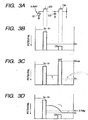
- Fig. 3A is an equivalent circuit showing the unit cell
- Figs. 3B to 3D are schematic potential diagrams for explanation of an example of the operation of the unit cell of the above x-ray image pickup device.
- the axis of abscissa represents locations on the unit cell
- the axis of ordinate represents potentials on the respective locations.
- Fig. 3B shows a potential diagram showing a sensor reset state.
- the potential of the storage capacity 122 becomes a reset voltage VV as shown in Fig. 3B .
- VA-VT symbol VT is a threshold voltage of the transistor 123.
- Fig. 3C is a potential diagram showing a signal storing state.
- Fig. 3D is a potential diagram showing a reading state.
- the transistor 124 turns on in a state where the output line reset transistor 150 is off, charges stored in the storage capacity 122 is read by the output line 125.
- Fig. 4 is a timing chart for explanation of an example of the driving operation of the x-ray image pickup device.
- a voltage given to the gate of the transistor 123 is a given voltage (voltage VA).
- Vv reset potential
- a pulse is added to ⁇ V1 by the horizontal scanning circuit 120, the signals stored in the storage capacity 122 are read to the respective output lines 125, and the respective horizontal scanning operations are conducted as ⁇ H1, ⁇ H2, ..., to thereby sequentially output signals from the output circuit 130 (Vout).
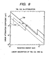
- Fig. 1 The absorption of x-rays by the semiconductor material of the x-ray sensor shown in Fig. 1 is determined by three mechanisms consisting of the photoelectric effect, Compton and electron pair creation.
- Fig. 5 shows examples of Si and Ge.
- the absorption is mainly determined by the photoelectric effect.
- the absorption coefficient of the x-rays becomes larger as the atomic number of the material is larger.
- the countermeasure to such a problem becomes necessary.
- a material 1 eV or more in band gap, small in dark current and large in x-ray absorption is desirable.
- GaAs, GaP and so on are preferable as the radiation detecting material since they are larger in band gap than Si.
- the x-ray absorption coefficient of Si is relatively small.
- Si may be used as a material for low energy.
- Fig. 6 shows an energy necessary for producing carriers due to the radiation of a semiconductor material.
- the axis of abscissa represents semiconductor energy gap, and the axis of ordinate represents energy necessary for the production. The smaller energy necessary for producing carriers is more desirable because a large number of carriers can be produced.
- the band gaps of GaAs and CdTe are about 5 Ev, respectively. Therefore, for example, 10000 pairs of carriers may be produced from an x-ray of 50 key.
- GaAs and CdTe are large in band gap, small in ⁇ (Ev), and large in x-ray absorption so that they are preferable as the radiation detecting material.
- GaAS is desirable as the applied material since the perfectivity of crystal is high and the dark current is small.
- GaAs has the x-ray absorbing characteristic considerably close to that of Ge. In view of the above characteristic, GaAs can be preferably employed for the medical application where the amount of irradiated x-rays is limited. The mass-productivity of GaAs is currently excellent similarly to Si and also very preferable economically.
- n + layer 30 and p + layer 10 on a portion that detects the x-rays become insensitive bands of the radiation (x-rays in this example).
- the conversion of the x-rays into carriers is effectively conducted in the depletion layer.
- Fig. 7 shows the applied voltage and the thickness of the depletion layer with n + or p resistivity of Si as a parameter. It is preferable that the resistivity is 100 ⁇ cm or more and the applied voltage is 10 V or higher, preferably 100 V or higher. The applied voltage of 1000 V or higher is demanded to provide the depletion layer close to 1 mm in thickness.
- a wafer of 107 ⁇ cm or more in resistance can be made of GaAs, a thicker depletion layer is obtained with a lower voltage as compared with Si, thereby being capable of making the sensitivity high.
- GaAs has the same x-ray absorbing characteristic as that of Ge, it is preferable directly as the x-ray material.
- a voltage of 1000 V or higher is applied to a terminal 1000 in case of Si. The voltage becomes lower in case of GaAs.
- the given voltage VA is always applied to the transistor (thin film transistor: TFT) 123, another electrode of the sensor cell 121 always becomes VA-VT. For that reason, a given voltage is always applied to the sensor cell 121 without any change of the depletion layer in thickness, thereby being capable of conducting stable operation.
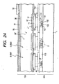
- Fig. 24 shows an example in which single crystal semiconductor is used as the high-resistive x-ray detecting portion.
- the material of the single crystal high resistant portion 20' is particularly preferably GaAs since the resistance is high (> 10 7 ⁇ cm), the dark current (band gap is 1.5 Ev) is small and a large-diameter wafer (6 inches ⁇ ) can be produced.
- Reference numeral 10' denotes an n + layer.
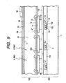
- Fig. 9 is a cross-sectional view showing an x-ray sensor in accordance with another embodiment of the present invention.
- a p region 500 (which forms a guard region) lower in density than p + of a p + layer 10 is disposed in the periphery of the p + layer 10.
- Fig. 10 is a cross-sectional view showing an x-ray sensor in accordance with still another embodiment of the present invention.
- Reference numeral 33 denotes an insulating film that separates the n + region 30.
- Fig. 11 is a schematically cross-sectional view showing an x-ray sensor in accordance with yet still another embodiment of the present invention.
- Fig. 11 shows an example such that a single crystal substrate is employed as the lower substrate.
- a single crystal substrate 114 is employed so as to dispose peripheral circuits on the lower substrate, thereby exhibiting the more effects of making the function higher and high-speed reading operation.
- the source and drain 102 which are n-type regions are formed within the single crystal substrate 114 which is a semiconductor substrate, and a gate electrode is formed on the p region 116 through the insulating layer, to thereby form a transistor 115.
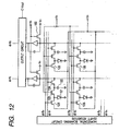
- Fig. 12 shows an equivalent circuit of an x-ray image pickup device in accordance with another embodiment of the present invention.
- a reset transistor 126 is connected to the sensor cell 121.
- the provision of the reset transistor (reset thin film transistor) 126 enables the residual image of the sensor to be improved.
- the voltage VRS is so set as to be slightly larger than VA-VT, to thereby provide an x-ray sensor improved in the residual image.
- the reset transistor 126 functions as potential fixing means for fixing the potential of the sensor cell 121 for a given period of time.
- Fig. 22 is a timing chart of the operation of the above x-ray image pickup device.
- the excessive voltage is, for example, a voltage larger than Vmax of the transistor 124 shown in Fig. 3C , and when the voltage of Vmax or higher is stored in the storage capacity C (122), the carriers flow to the output side of the transistor 124, to thereby have great influence on an image. An influence on the image which is called "blooming" by CCD can be eliminated.
- Fig. 13 is a diagram showing an example in which the reset switch 127 that resets the storage capacity is disposed in each of the storage capacities.
- the storage capacity 122 (capacitance C1) can be prevented from becoming a voltage of VB - VTH or higher.
- the overflow of the carriers in the storage capacity 122 from the read transistor 124 is prevented, thereby being capable of improving the characteristic of a longitudinal image.
- the voltage in the off-state may be a complete off-state potential.
- the above function can bring a protective function when the excessive x-rays are inputted to the device.
- the switching transistor 127 can provide two functions of the reset switch and the protecting circuit for preventing the carrier overflow.
- Fig. 14 is a diagram for explanation of an embodiment in which the transistors 126 and 127 are disposed together.
- Q max can be readily changed with a change in V A , V B and V R . Also, if V B is set by a smaller one of the source-gate withstand voltage (V S - G max ) of the switching transistor 124 and the withstand voltage (V S -D max ) between the source and the drain thereof, the voltage breakdown of the switching transistor can be protected.
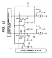
- a source follower is provided for each of cells, that is, an amplifier is provided for each of cells, a signal can be amplified so that the sensitivity can be improved.
- Each of the cells has a transistor 128 for selection and a transistor 129 for amplification to constitute the source follower.
- Figs. 16 and 18 show the unit cells structured as shown in Figs. 12 and 14 , with the source follower shown in Fig. 15 .
- the reset transistor 126 is disposed, respectively, to thereby improve a residual image.
- Fig. 19 shows an embodiment in which two output systems are disposed in order to remove a fixed pattern.
- noises after the sensor has been reset are read from each cell and then stored in the storage capacity C N through a transistor 131.
- a signal including the noise component is read from the cell through the transistor 132 and then stored in the storage capacity C s .
- the noises and the signal including the noise component are read from both of the storage capacities C N and C S , and the noise component is subtracted from the signal including the noise component and then outputted by a subtracting amplifier 137 (Vout).
- Reference numeral 133 and 134 denote transistors that reset the storage capacities C N and C S .
- Fig. 25 is a schematically cross-sectional view showing an x-ray sensor in accordance with the present invention.
- the same reference numerals as those in Fig. 1 are identical with those described with reference to Fig. 1 , and therefore, their details will be omitted.
- the x-ray sensor shown in Fig. 25 produces pairs of electrons and positive holes from x-rays irradiated onto the sensing portion 100, stores either of the carriers of the electrons and the positive holes, and reads the carriers as an electric signal representative of image information, as described with reference to Fig. 1 .
- the x-ray sensing portion 100 is made of semiconductor such as GaAs, GaP or Si as described above, and includes an n + layer 310, a p - layer (i layer) 320 and p + layer 330. Those layers form a p-i-n diode where a depletion layer extends from an interface of the n + layer 310 and the p - layer (i layer) 320.
- Metal layers 31 and 32 are formed on the p + layer 330, that is, the x-ray incident side, and metal layers 11 and 12 are formed under the n + layer 310, that is, on an opposite side of the x-ray incident side, in this example, on the reading portion 200 side.
- the metal layer 12 is made of a barrier metal as described above.
- the x-ray sensing portion 100 may be formed by using the single crystal semiconductor substrate. As shown in the figure, this example is different from the example shown in Figs. 1 and 2 in the connecting direction of the diode in the x-ray sensing portion 100.
- the reading portion 200 includes an n-type thin film transistor 220 that constitutes a circuit on the insulating substrate 1, and the n-type thin film transistor 220 includes a gate 221, an n + source, an n + drain 222, a semiconductor active layer 223 of the low impurity density, and a metal wiring 230 connected with its source and its drain.
- the thin film transistor 220 is covered with the protective film 113.
- the preferred semiconductor material of the thin film transistor may be non-single crystal material such as amorphous silicon, polysilicon or microcrystal silicon.
- the reading portion 200 is formed with a capacitance that forms a storage capacity.
- Fig. 26 is a schematically equivalent circuit diagram showing an x-ray image pickup device having the x-ray sensor shown in Fig. 25 .
- the unit cell includes an x-ray sensor cell 121, a storage capacity 122, a first n-type thin film transistor (TFT) 123 that transfers a signal from the x-ray sensor cell 121 to the storage capacity 122, and a second n-type thin film transistor 124 that reads a signal from the storage capacity 122.
- TFT thin film transistor
- the polarity of the x-ray sensor cell 121 shown as a diode in the figure is different from the polarity of the equivalent circuit diagram shown in Fig. 2 .
- the second thin film transistor 124 in each of the unit cells is selected every row by a horizontal scanning circuit (a shift register, or the like) 120, and a signal is read from the storage capacity 122 in each of the unit cells to an output line 125.
- the signal is inputted to an output circuit 130 through an amplifier 140 which is connected to the output line 125 and then sequentially outputted for each of columns by the output circuit 130.
- the connection of the amplifier 140 to each of the signal lines is effective for the following reasons.
- the parasitic capacitance consisting of the capacitance between the wiring cross portion of the output line and the gate of the thin film transistor and the source connected to the output line, etc.
- the ratio of the signal to the noise is sufficiently large.
- the respective storage capacities 122 and the respective output lines 125 are set to a potential Vv through the transistor 124 by the output line reset transistor 150.
- the output circuit 130 includes, for example, a sampling storage capacity 160 and a transistor 170 that connects the sampling storage capacity and the common output line, which are disposed for each of the output lines (refer to the schematic circuit diagram shown in Fig. 35 ).
- the electric signals from the output line are sequentially stored in the sampling storage capacity 160 in response to a transfer pulse ⁇ T, and timing pulses of ⁇ H1, ⁇ H2, Vietnamese are sequentially inputted to the transistors 180 in the circuit from a scanning circuit 195 such as a shift register, to thereby sequentially turn on the transistors 180, and the signals are read to the buffer amplifier 190 connected to the common output line from the sampling storage capacity 160 for each of the columns and then outputted (V OUT ).
- a scanning circuit 195 such as a shift register
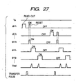
- Fig. 27 shows an example of a timing chart for driving the x-ray image pickup device shown in Fig. 26 .
- a voltage given to the gate of the transistor 123 is a given voltage (voltage VA).
- the output line reset transistor 150 connected to the reset potential V V turns on with ⁇ V R as V R , and ⁇ V 1 turns on at the same time (reset mode).
- ⁇ V R and ⁇ V 1 turn off, and the x-ray sensor cell 121 comes to a storage mode.
- a pulse is added to ⁇ V 1 by the horizontal scanning circuit 120, and the signals stored in the storage capacity 122 are read to the respective output lines 125 (read mode).
- the above cycle is conducted with respect to the respective horizontal lines in the same manner to sequentially read the information.
- other operation may be conducted in the same manner as that in Fig. 27 .
- the above operation can prevent a phenomenon (phenomenon called "blooming" by CCD or the like) in which the electric charges are leaked to the output lines from the storage capacities through the switches 124 and adversely affect other cell reading operation when intense radiations are made incident to a part of the image pickup region of the image pickup device.
- the p + layer 330 and n + layer 310 on a portion that detects the x-rays become insensitive bands of the radiation.
- the conversion of the x-rays into carriers is effectively conducted in the depletion layer.
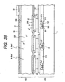
- Fig. 28 is a schematically cross-sectional view showing another example of an x-ray sensor in accordance with the present invention.
- this embodiment shows an example in which the x-ray sensing portion 100 of the x-ray sensor shown in Fig. 24 is different in polarity, and shows an example in which a p - type or i-type single crystal semiconductor is used as the high-resistive x-ray detecting portion.
- the material of the single crystal high resistant portion (p - region in this example) 320 is preferably GaAs since the resistance is high (> 10 7 ⁇ cm), the dark current (band gap is 1.5 Ev) is small, and a large-diameter wafer (6 inches ⁇ ) can be produced.
- Reference numeral 310 denotes an n + layer, and 330 is a p + region.
- Fig. 29 is a schematically cross-sectional view showing another example of an x-ray sensor in accordance with the present invention.
- This embodiment shows an example in which the x-ray sensing portion 100 of the x-ray sensor shown in Fig. 29 is different in polarity, and shows an example in which a p - type or i-type single crystal semiconductor (p - region is the figure) is used as the high-resistive x-ray detecting portion.
- a p - type or i-type single crystal semiconductor p - region is the figure
- an n region 3500 (which forms a guard region) lower in density than n + of an n + layer 310 is disposed in the periphery of the n + layer 310.
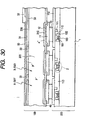
- Fig. 30 is a schematically cross-sectional view showing another example of an x-ray sensor in accordance with the present invention.
- This embodiment shows an example in which the x-ray sensing portion 100 of the x-ray sensor shown in Fig. 29 is different in polarity, and shows an example in which a p - type or i-type single crystal semiconductor (the p - region 320 in the figure) is used as the high-resistive x-ray detecting portion.
- a p + region 330 is separated with the effect of improving the resolution.
- Reference numeral 33 denotes an insulating film that separates the p + region 30.
- n - region 320 is made reverse electrically conductive type n - , because the depletion layer extends from the surface side and a depletion layer is disposed on a portion to which the x-rays are surely frequently made incident, the sensitivity and the resolution are stabilized. However, there is required that the depletion layer extends over the entire thickness of the n - region between p + and n + .
- Fig. 31 is a schematically cross-sectional view showing an x-ray sensor in accordance with another embodiment of the present invention.
- Fig. 31 shows an example in which the lower substrate of the x-ray sensor shown in Fig. 28 is formed of a single crystal substrate, and shows an example in which the x-ray sensor shown in Fig. 11 is different in polarity of the x-ray sensing portion 100.
- the peripheral circuits can be disposed on the lower substrate, thus further exhibiting the effects of making the function high and reading at a high speed.
- the transistor 115 is formed by forming a gate electrode on the p region 116.
- Fig. 32 is a schematically cross-sectional view showing another example of an x-ray sensor in accordance with the present invention.
- an n-type region 311 lower in the density of impurities than the n + region 310 is disposed in the entire periphery of the n + region 310.
- the electric field in the periphery of the n + region 310 at the p-n junction is reduced, thereby being capable of improving the withstand voltage of the p-n junction and reducing the dark current in the depletion layer region.
- Fig. 33 is a schematically equivalent circuit diagram for explanation of another example of an x-ray image pickup device in accordance with the present invention.
- This embodiment shows an example in which the sensor cell 121 in the schematically equivalent circuit diagram shown in Fig. 12 is reversed in polarity.
- Fig. 34 is a timing chart for explanation of an example of the driving operation of the above x-ray image pickup device.
- the excessive voltage is, for example, a voltage larger than V max of the thin film transistor 124 shown in Fig. 3C , and when the voltage of V max or higher is stored in the storage capacity (C) 122, the carriers flow out to the output side of the transistor 124, to thereby have great influence on an image.
- An influence on the image which is called "blooming" by CCD can be eliminated by thus controlling the driving operation of the transistor 126.
- Fig. 20 is a schematically perspective view showing one example in which a plurality of x-ray sensing portions 100 are combined together on a substrate 200 on which a reading circuit and so on formed on an insulating substrate are formed, to thereby fabricate a large-screen radiation image pickup device.
- reference numerals 1500 and 1600 denote a driver circuit and an output circuit, respectively, which are located on the reading portion 200 which functions as a circuit substrate portion.
- a glass substrate is used as the substrate 1 of the reading portion 200, thereby being capable of making the size of the image pickup device large.
- Fig. 21 is a schematic diagram showing an example of a medical diagnosing device using an image pickup device of the present invention.
- reference numeral 1001 denotes an x-ray tube as an x-ray generation source
- 1002 is an x-ray shutter that controls the open/close of the x-ray penetration
- 1003 is an irradiation cylinder or a movable diaphragm
- 1004 is an object to be photographed
- 1005 is a radiation detector according to the present invention
- 1006 is a data processing unit that data-processes a signal from the radiation detector 1005.
- Reference numeral 1007 denotes a computer that displays an x-ray image, etc.
- a display 1009 such as CRT on the basis of a signal from the data processing unit 1006, and controls the x-ray tube 1001 through a camera controller 1010, an x-ray controller 1011 and a capacitor-type high-voltage generator 1012 to control the amount of generated x-rays.
- the present invention provides the following advantages.
Landscapes
- Engineering & Computer Science (AREA)
- Multimedia (AREA)
- Signal Processing (AREA)
- Solid State Image Pick-Up Elements (AREA)
- Measurement Of Radiation (AREA)
- Transforming Light Signals Into Electric Signals (AREA)
Claims (14)
- Strahlungsbildaufnahmevorrichtung mit:einer Vielzahl von Eingabebildpunkten, die eine Elektrische-Ladung-Umwandlungseinrichtung (121) zum Umwandeln einer einfallenden Strahlung in elektrische Ladungen, eine Elektrische-Ladung-Speichereinrichtung (122) zum Speichern der durch die Elektrische-Ladung-Umwandlungseinrichtung umgewandelten elektrischen Ladungen, eine zwischen der Elektrische-Ladung-Umwandlungseinrichtung und der Elektrische-Ladung-Speichereinrichtung bereitgestellte Steuereinrichtung (123) zum Steuern eines an die Elektrische-Ladung-Umwandlungseinrichtung angelegten elektrischen Feldes, und eine Leseeinrichtung (124, 129) zum Lesen eines Signals basierend auf den in der Elektrische-Ladung-Speichereinrichtung gespeicherten elektrischen Ladungen aufweisen;einer an die Vielzahl von Eingabebildpunkten angeschlossenen Ausgabeleitung (125) zum Ausgeben des von der Vielzahl von Eingabebildpunkten gelesenen Signals; undeiner Schalteinrichtung (124, 150; 127; 124, 126, 127; 123, 126; 123, 126, 127; 123, 124, 126, 150) zum Zurücksetzen der Elektrische-Ladung-Speichereinrichtung;dadurch gekennzeichnet, dasszumindest die Steuereinrichtung, die Elektrische-Ladung-Speichereinrichtung und die Leseeinrichtung auf demselben isolierenden Substrat ausgebildet sind, die Elektrische-Ladung-Umwandlungseinrichtung auf der Steuereinrichtung, der Elektrische-Ladung-Speichereinrichtung und der Leseeinrichtung laminiert ist, und zumindest die Steuereinrichtung und die Leseeinrichtung Dünnfilmtransistoren aufweisen.
- Strahlungsbildaufnahmevorrichtung nach Anspruch 1, wobei das auf den elektrischen Ladungen basierende Signal ein auf einem Potential basierendes Signal ist.
- Strahlungsbildaufnahmevorrichtung nach Anspruch 1 oder 2, ferner mit einer Sensorpotentialfixierungseinrichtung (126) zum Einstellen des Potentials eines Anschlusses der Elektrische-Ladung-Umwandlungseinrichtung (121) auf ein gewünschtes Potential.
- Strahlungsbildaufnahmevorrichtung nach einem der Ansprüche 1 bis 3, wobei die Schalteinrichtung an eine Gespeichertes-Potential-Fixierungseinrichtung angeschlossen ist, um das Potential von einem Anschluss der Elektrische-Ladung-Speichereinrichtung auf ein gewünschtes Potential einzustellen.
- Strahlungsbildaufnahmevorrichtung nach einem der Ansprüche 1 bis 4, wobei ein Ende der Schalteinrichtung an die Ausgabeleitungsseite angeschlossen ist, und das andere Ende der Schalteinrichtung an eine Gespeichertes-Potential-Fixierungseinrichtung angeschlossen ist, um das Potential eines Anschlusses der Elektrische-Ladung-Speichereinrichtung (122) auf ein gewünschtes Potential einzustellen.
- Strahlungsbildaufnahmevorrichtung nach einem der Ansprüche 1 bis 5, wobei die Elektrische-Ladung-Umwandlungseinrichtung (121) eine p-n-Struktur aufweist, zumindest die Steuereinrichtung (123) und die Leseeinrichtung (124, 129) n-Typ-Dünnfilmtransistoren aufweisen, ein Anschluss des n-Bereichs der p-n-Übergangszone an Source oder Drain des n-Typ-Dünnfilmtransistors der Steuereinrichtung elektrisch angeschlossen ist, ein Anschluss des p-Bereichs der p-n-Übergangszone an eine Vorspannungseinrichtung angeschlossen ist, und die p-n-Übergangszone in Sperrrichtung vorgespannt ist, so dass eine zum Erfassen der Strahlung ausreichende Sperrschicht in dem Halbleitersubstrat ausgebildet wird.
- Strahlungsbildaufnahmevorrichtung nach einem der Ansprüche 1 bis 6, wobei die Eingabebildpunkte in einer zweidimensionalen Matrix angeordnet sind.
- Strahlungsbildaufnahmevorrichtung nach einem der Ansprüche 1 bis 7, ferner mit einer Einrichtung zum Speichern eines Signals einschließlich einer Bildinformationskomponente und einer Rauschkomponente, einer Einrichtung zum Speichern der Rauschkomponente, und einer Einrichtung zum Subtrahieren der Rauschkomponente von dem Signal einschließlich der Bildinformationskomponente und der Rauschkomponente.
- Strahlungsbildaufnahmevorrichtung nach einem der Ansprüche 1 bis 8, wobei die Elektrische-Ladung-Umwandlungseinrichtung (121) auf einem Halbleiter-Einkristall-Substrat gefertigt ist, und das Halbleitersubstrat eine Energiebandlücke von 1 Ev oder mehr in einer Bandlücke aufweist.
- Strahlungsbildaufnahmevorrichtung nach Anspruch 1, ferner mit einer Sensorpotentialfixierungseinrichtung (126) zum Einstellen des Potentials eines Anschlusses der Elektrische-Ladung-Umwandlungseinrichtung (121) und/oder des Potentials eines Anschlusses der Elektrische-Ladung-Speichereinrichtung (122) auf ein gewünschtes Potential;
wobei die Sensorpotentialfixierungseinrichtung ein konstantes Potential liefert, wenn die Sensorpotentialfixierungseinrichtung ausgeschaltet ist, und, wenn das Potential der Elektrische-Ladung-Speichereinrichtung ein überschüssiges Potential ist, die Potentialfixierungseinrichtung als Ablenkeinrichtung zum Ablenken der überschüssigen elektrischen Ladungen dient. - Strahlungsbildaufnahmevorrichtung nach einem der Ansprüche 1 bis 10, wobei
die Elektrische-Ladung-Speichereinrichtung (122) zurückgesetzt wird, wenn zumindest die Schalteinrichtung und die Leseeinrichtung (124, 129) zur selben Zeit eingeschaltet sind;
die aufgrund der einfallenden Strahlung durch die Elektrische-Ladung-Umwandlungseinrichtung (121) erzeugten elektrischen Ladungen in der Elektrische-Ladung-Speichereinrichtung gespeichert werden, wenn die Schalteinrichtung und die Leseeinrichtung ausgeschaltet sind; und
ein elektrisches Ladungssignal von der Speichereinrichtung an die Ausgabeleitungen ausgegeben wird, wenn die Leseeinrichtung eingeschaltet ist und die Schalteinrichtung ausgeschaltet ist. - Strahlungsbildaufnahmevorrichtung nach Anspruch 11, wobei die Ausgabeleitungen zwischen der Lese- und der Ausgabeoperation zurückgesetzt werden, wenn die Schalteinrichtung eingeschaltet ist und die Leseeinrichtung (124, 129) ausgeschaltet ist.
- Strahlungsbildaufnahmevorrichtung nach einem der Ansprüche 1 bis 12, wobei die Dünnfilmtransistoren Nicht-Einkristallhalbleiter aufweisen.
- Strahlungsbildaufnahmevorrichtung nach einem der Ansprüche 1 bis 13, wobei zumindest die Steuereinrichtung (123), die Speichereinrichtung (122) und die Leseeinrichtung (124, 129) auf einer Seite des isolierenden Substrats dieselbe Schichtstruktur aufweisen wie eine untere Elektrode, ein isolierender Film, ein hochohmiger Halbleiterfilm, ein niederohmiger Halbleiterfilm und eine obere Elektrode.
Applications Claiming Priority (2)
| Application Number | Priority Date | Filing Date | Title |
|---|---|---|---|
| JP21741099 | 1999-07-30 | ||
| JP21741099 | 1999-07-30 |
Publications (3)
| Publication Number | Publication Date |
|---|---|
| EP1073267A2 EP1073267A2 (de) | 2001-01-31 |
| EP1073267A3 EP1073267A3 (de) | 2009-04-22 |
| EP1073267B1 true EP1073267B1 (de) | 2010-12-22 |
Family
ID=16703775
Family Applications (1)
| Application Number | Title | Priority Date | Filing Date |
|---|---|---|---|
| EP00306411A Expired - Lifetime EP1073267B1 (de) | 1999-07-30 | 2000-07-27 | Strahlungsbildaufnahmeapparatus |
Country Status (3)
| Country | Link |
|---|---|
| US (1) | US6489618B1 (de) |
| EP (1) | EP1073267B1 (de) |
| DE (1) | DE60045404D1 (de) |
Families Citing this family (11)
| Publication number | Priority date | Publication date | Assignee | Title |
|---|---|---|---|---|
| JP3631114B2 (ja) * | 2000-08-01 | 2005-03-23 | キヤノン株式会社 | 撮像装置 |
| JP3840050B2 (ja) * | 2000-11-01 | 2006-11-01 | キヤノン株式会社 | 電磁波変換装置 |
| JP2002148342A (ja) * | 2000-11-07 | 2002-05-22 | Canon Inc | 放射線撮像装置 |
| US6765187B2 (en) * | 2001-06-27 | 2004-07-20 | Canon Kabushiki Kaisha | Imaging apparatus |
| JP2003240861A (ja) * | 2002-02-20 | 2003-08-27 | Canon Inc | 放射線検出素子、放射線撮像装置及び放射線検出方法 |
| US7214945B2 (en) * | 2002-06-11 | 2007-05-08 | Canon Kabushiki Kaisha | Radiation detecting apparatus, manufacturing method therefor, and radiation image pickup system |
| DE60336291D1 (de) * | 2002-11-13 | 2011-04-21 | Canon Kk | Bildaufnahmevorrichtung, Strahlungsbildaufnahmevorrichtung und Strahlungsbildaufnahmesystem |
| CN100502021C (zh) * | 2005-06-13 | 2009-06-17 | 佳能株式会社 | 电磁辐射检测设备、辐射检测设备和系统及激光处理方法 |
| JP5013754B2 (ja) * | 2005-06-13 | 2012-08-29 | キヤノン株式会社 | 電磁波検出装置、放射線検出装置、放射線検出システム及びレーザ加工方法 |
| JP5196739B2 (ja) * | 2006-06-09 | 2013-05-15 | キヤノン株式会社 | 放射線撮像装置及び放射線撮像システム |
| JP6247918B2 (ja) * | 2013-12-09 | 2017-12-13 | 浜松ホトニクス株式会社 | 放射線イメージセンサ |
Family Cites Families (9)
| Publication number | Priority date | Publication date | Assignee | Title |
|---|---|---|---|---|
| US5401952A (en) | 1991-10-25 | 1995-03-28 | Canon Kabushiki Kaisha | Signal processor having avalanche photodiodes |
| JPH05211321A (ja) | 1991-10-25 | 1993-08-20 | Canon Inc | アバランシェフォトダイオード、及びそれを具備する信号処理装置 |
| US5452004A (en) | 1993-06-17 | 1995-09-19 | Litton Systems, Inc. | Focal plane array imaging device with random access architecture |
| US5442176A (en) * | 1993-10-06 | 1995-08-15 | Raytheon Company | Infrared detector array |
| JP3066944B2 (ja) * | 1993-12-27 | 2000-07-17 | キヤノン株式会社 | 光電変換装置、その駆動方法及びそれを有するシステム |
| JP3897389B2 (ja) * | 1996-02-22 | 2007-03-22 | キヤノン株式会社 | 光電変換装置の駆動方法及び光電変換装置 |
| JP3559640B2 (ja) * | 1996-02-27 | 2004-09-02 | キヤノン株式会社 | 光電変換装置 |
| US5986297A (en) * | 1996-05-22 | 1999-11-16 | Eastman Kodak Company | Color active pixel sensor with electronic shuttering, anti-blooming and low cross-talk |
| TW421962B (en) * | 1997-09-29 | 2001-02-11 | Canon Kk | Image sensing device using mos type image sensing elements |
-
2000
- 2000-07-27 US US09/627,446 patent/US6489618B1/en not_active Expired - Lifetime
- 2000-07-27 EP EP00306411A patent/EP1073267B1/de not_active Expired - Lifetime
- 2000-07-27 DE DE60045404T patent/DE60045404D1/de not_active Expired - Lifetime
Also Published As
| Publication number | Publication date |
|---|---|
| DE60045404D1 (de) | 2011-02-03 |
| EP1073267A3 (de) | 2009-04-22 |
| EP1073267A2 (de) | 2001-01-31 |
| US6489618B1 (en) | 2002-12-03 |
Similar Documents
| Publication | Publication Date | Title |
|---|---|---|
| EP0660421B9 (de) | Photoelektrischer Umwandler, sein Steuerverfahren und System mit diesem photoelektrischen Umwandler | |
| US6730914B2 (en) | Photoconductor-on-active-pixel (POAP) sensor utilizing equal-potential pixel electrodes | |
| US6707066B2 (en) | Radiation image pick-up device | |
| JP2594992B2 (ja) | 固体撮像装置 | |
| EP1009038B1 (de) | Strahlungsermittlungsvorrichtung | |
| US8039809B2 (en) | Sensor panel and image detecting device | |
| EP1583150A1 (de) | Bildsensor mit grossflächigen, hochgeschwindigen, hochempfindlichen Pixeln | |
| JP2001345440A (ja) | 電磁波検出装置 | |
| EP1073267B1 (de) | Strahlungsbildaufnahmeapparatus | |
| US6399950B1 (en) | Two-dimensional radiation detector | |
| KR20010067103A (ko) | 방사선 검출장치 | |
| US8779377B2 (en) | Image pickup unit and image pickup display system | |
| JP2003168794A (ja) | 放射線検出素子、放射線撮像装置、放射線検出方法、及び放射線撮像方法 | |
| US20030155517A1 (en) | Radiation detecting element, radiation image pickup apparatus and radiation detecting method | |
| EP4332638A1 (de) | Lichtempfangselement, röntgenbildgebungselement und elektronische vorrichtung | |
| JP3689619B2 (ja) | 放射線撮像装置 | |
| KR100642655B1 (ko) | 방사선 검출장치 | |
| JP2000111653A (ja) | 放射線2次元検出器 | |
| JPH0430577A (ja) | 固体撮像素子 | |
| JP2002246577A (ja) | X線画像検出器 | |
| JPS617662A (ja) | 固体撮像素子 |
Legal Events
| Date | Code | Title | Description |
|---|---|---|---|
| PUAI | Public reference made under article 153(3) epc to a published international application that has entered the european phase |
Free format text: ORIGINAL CODE: 0009012 |
|
| AK | Designated contracting states |
Kind code of ref document: A2 Designated state(s): AT BE CH CY DE DK ES FI FR GB GR IE IT LI LU MC NL PT SE |
|
| AX | Request for extension of the european patent |
Free format text: AL;LT;LV;MK;RO;SI |
|
| PUAL | Search report despatched |
Free format text: ORIGINAL CODE: 0009013 |
|
| AK | Designated contracting states |
Kind code of ref document: A3 Designated state(s): AT BE CH CY DE DK ES FI FR GB GR IE IT LI LU MC NL PT SE |
|
| AX | Request for extension of the european patent |
Extension state: AL LT LV MK RO SI |
|
| 17P | Request for examination filed |
Effective date: 20091022 |
|
| AKX | Designation fees paid |
Designated state(s): DE FR GB IT NL |
|
| 17Q | First examination report despatched |
Effective date: 20091218 |
|
| GRAP | Despatch of communication of intention to grant a patent |
Free format text: ORIGINAL CODE: EPIDOSNIGR1 |
|
| GRAS | Grant fee paid |
Free format text: ORIGINAL CODE: EPIDOSNIGR3 |
|
| GRAA | (expected) grant |
Free format text: ORIGINAL CODE: 0009210 |
|
| AK | Designated contracting states |
Kind code of ref document: B1 Designated state(s): DE FR GB IT NL |
|
| REG | Reference to a national code |
Ref country code: GB Ref legal event code: FG4D |
|
| REF | Corresponds to: |
Ref document number: 60045404 Country of ref document: DE Date of ref document: 20110203 Kind code of ref document: P |
|
| REG | Reference to a national code |
Ref country code: DE Ref legal event code: R096 Ref document number: 60045404 Country of ref document: DE Effective date: 20110203 |
|
| REG | Reference to a national code |
Ref country code: NL Ref legal event code: VDEP Effective date: 20101222 |
|
| PG25 | Lapsed in a contracting state [announced via postgrant information from national office to epo] |
Ref country code: NL Free format text: LAPSE BECAUSE OF FAILURE TO SUBMIT A TRANSLATION OF THE DESCRIPTION OR TO PAY THE FEE WITHIN THE PRESCRIBED TIME-LIMIT Effective date: 20101222 |
|
| PLBE | No opposition filed within time limit |
Free format text: ORIGINAL CODE: 0009261 |
|
| STAA | Information on the status of an ep patent application or granted ep patent |
Free format text: STATUS: NO OPPOSITION FILED WITHIN TIME LIMIT |
|
| 26N | No opposition filed |
Effective date: 20110923 |
|
| PG25 | Lapsed in a contracting state [announced via postgrant information from national office to epo] |
Ref country code: IT Free format text: LAPSE BECAUSE OF FAILURE TO SUBMIT A TRANSLATION OF THE DESCRIPTION OR TO PAY THE FEE WITHIN THE PRESCRIBED TIME-LIMIT Effective date: 20101222 |
|
| REG | Reference to a national code |
Ref country code: DE Ref legal event code: R097 Ref document number: 60045404 Country of ref document: DE Effective date: 20110923 |
|
| REG | Reference to a national code |
Ref country code: FR Ref legal event code: ST Effective date: 20120330 |
|
| PG25 | Lapsed in a contracting state [announced via postgrant information from national office to epo] |
Ref country code: FR Free format text: LAPSE BECAUSE OF NON-PAYMENT OF DUE FEES Effective date: 20110801 |
|
| PGFP | Annual fee paid to national office [announced via postgrant information from national office to epo] |
Ref country code: DE Payment date: 20130731 Year of fee payment: 14 |
|
| PGFP | Annual fee paid to national office [announced via postgrant information from national office to epo] |
Ref country code: GB Payment date: 20130712 Year of fee payment: 14 |
|
| REG | Reference to a national code |
Ref country code: DE Ref legal event code: R119 Ref document number: 60045404 Country of ref document: DE |
|
| GBPC | Gb: european patent ceased through non-payment of renewal fee |
Effective date: 20140727 |
|
| PG25 | Lapsed in a contracting state [announced via postgrant information from national office to epo] |
Ref country code: DE Free format text: LAPSE BECAUSE OF NON-PAYMENT OF DUE FEES Effective date: 20150203 |
|
| REG | Reference to a national code |
Ref country code: DE Ref legal event code: R119 Ref document number: 60045404 Country of ref document: DE Effective date: 20150203 |
|
| PG25 | Lapsed in a contracting state [announced via postgrant information from national office to epo] |
Ref country code: GB Free format text: LAPSE BECAUSE OF NON-PAYMENT OF DUE FEES Effective date: 20140727 |