EP1076362A2 - Halbleiterschaltung - Google Patents
Halbleiterschaltung Download PDFInfo
- Publication number
- EP1076362A2 EP1076362A2 EP00117082A EP00117082A EP1076362A2 EP 1076362 A2 EP1076362 A2 EP 1076362A2 EP 00117082 A EP00117082 A EP 00117082A EP 00117082 A EP00117082 A EP 00117082A EP 1076362 A2 EP1076362 A2 EP 1076362A2
- Authority
- EP
- European Patent Office
- Prior art keywords
- transistor
- operating voltage
- circuit according
- ground
- source
- Prior art date
- Legal status (The legal status is an assumption and is not a legal conclusion. Google has not performed a legal analysis and makes no representation as to the accuracy of the status listed.)
- Withdrawn
Links
Images

Classifications
-
- H—ELECTRICITY
- H10—SEMICONDUCTOR DEVICES; ELECTRIC SOLID-STATE DEVICES NOT OTHERWISE PROVIDED FOR
- H10D—INORGANIC ELECTRIC SEMICONDUCTOR DEVICES
- H10D89/00—Aspects of integrated devices not covered by groups H10D84/00 - H10D88/00
- H10D89/60—Integrated devices comprising arrangements for electrical or thermal protection, e.g. protection circuits against electrostatic discharge [ESD]
- H10D89/601—Integrated devices comprising arrangements for electrical or thermal protection, e.g. protection circuits against electrostatic discharge [ESD] for devices having insulated gate electrodes, e.g. for IGFETs or IGBTs
- H10D89/811—Integrated devices comprising arrangements for electrical or thermal protection, e.g. protection circuits against electrostatic discharge [ESD] for devices having insulated gate electrodes, e.g. for IGFETs or IGBTs using FETs as protective elements
Definitions
- the invention relates to a circuit according to the preamble of claim 1.
- Such a circuit is provided, for example, in integrated circuits as they are used as sensors in the automotive industry, for example own patent application EP 0 648 019 A2 (internal file number: C-1463EP).
- the On-board voltages are usually in the motor vehicle sector due to the 12 volt battery voltage given. In real operation, however, there may be significant deviations result at the top and bottom of this value. The operating voltages to be observed between 5 volts to 24 volts or even outside these limits.
- external and / or internal protective measures e.g. internal voltage stabilization devices and an increased dielectric strength of the circuit due to an adapted Circuit design and use of internal surge protective devices, these high operating voltages can be permitted.
- the circuit can be operated without further protective measures destroyed or damaged, for example due to a thermal Overload due to excessive currents in the event of breakdown or damage to transistors due to excessive stress voltages.
- the circuit known from EP 0 648 019 A2 has some protection against such reverse polarity by the reverse current is limited by an internal or external resistor.
- the invention has for its object to further develop the protective device of the type mentioned in such a way that protection against reverse polarity is also possible in those circuits in which the use of the known protective device above is not possible; Furthermore, the further development should be monolithically integrable with the actual circuit so that external polarity reversal protection devices are eliminated and overvoltages in the event of polarity reversal are harmless for the entire circuit arrangement.
- the invention proposes that the circuit according to the preamble of claim 1 is designed in accordance with the characterizing part of this claim 1.
- the basic idea of the invention is between the inner ground connection (This means the usual ground connection on the chip of the monolithically integrated Circuit) and the connection for the external ground a transistor on the chip in addition insert.
- This should be conductive in normal operation and in the event of polarity reversal, namely in the event of concerns the operating voltage on the ground connection line and the ground on the operating voltage line, not be a leader.
- the incorrectly applied operating voltage not on the actual circuit so that it is now protected and not destroyed becomes. So that the reverse polarity does not destroy the transistor even by high voltages is implemented as a high-voltage transistor.
- a major advantage of this Protective device is that no current flows in the event of reverse polarity.
- a preferred embodiment of the invention for a standard CMOS manufacturing process provides that the transistor used for reverse polarity protection as MOS transistor is formed with an n-type channel. Its source and drain electrodes are, as usual, embedded in relatively heavily doped areas that are opposite Are conductivity type like the p-type substrate. The one in normal operation, i.e. without Reverse polarity, the transistor region serving as the source region is in turn in a relative lightly doped n-well embedded, which is arranged laterally and below the source region and of the same conductivity type as the transistor and of the opposite Conductivity type as the substrate is. In normal operation, i.e. without reverse polarity, is formed conductive channel between source and drain.
- the transistor is thus conductive and suitable large design, almost no voltage drops across its drain-source path from. In the event of reverse polarity, source becomes drain and drain becomes source and the transistor blocked via its control electrode, whereby a conductive channel is no longer present.
- the applied operating voltage essentially falls over the weakly doped n-well so that no sensitive field strength on the sensitive gate oxide leads to damage of the transistor leads, can occur.
- the transistor is an enhancement-type n-channel MOSFET (Enrichment type), wherein advantageously the tub for embedding the Source area - Source is here related to the unpoled normal operating case - relative weak, e.g. n - endowed; is. It is also conceivable to use a further transistor for protection against reverse polarity not only in the ground connection line but also in the operating voltage line insert. This transistor is then of the other conductivity type, for example, a p-channel MOSFET.
- the signal outputs of the inner circuit with the associated transistors are also by the transistor specified above as an exemplary embodiment against reverse polarity the operating voltage protected.
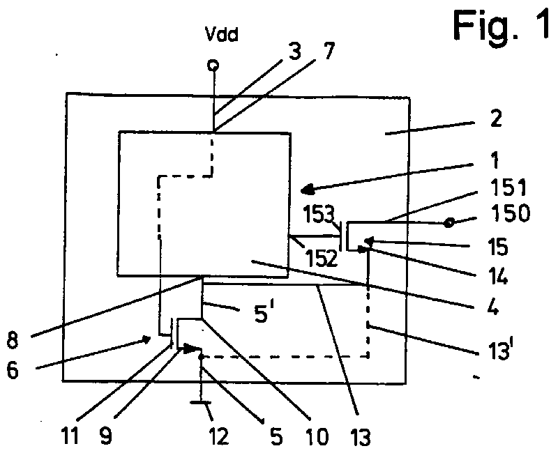
- the circuit 1 according to the invention shown in FIG. 1 is arranged within a circuit 2, in particular a monolithically integrated circuit.
- the circuit 1 has an operating voltage line 3, an internal circuit arrangement 4 to be protected, a ground connection line 5 and a transistor 6 as a polarity protection device.
- the operating voltage line 3 is connected to an input 7 of the internal circuit arrangement 4.
- An output 8 of the internal circuit arrangement 4 is connected to the ground connecting line 5 via the transistor 6.
- the transistor 6 has a source electrode 9, a drain electrode 10 and a gate electrode 11.
- the source electrode 9 is connected via the ground connection line 5 to the connection for an external ground 12.
- the drain electrode 10 is connected via line 5 'to the connection 8 for the inner "ground of the internal circuit arrangement 4.
- the gate electrode 11 is coupled to the internal circuit arrangement 4 and has, for example, the positive operating voltage Vdd as drive potential in normal operation.
- the drain electrode 10 of the transistor 6 via a line 13 to a source terminal 14 of a transistor 15 connected, which has an open-drain output 151 and its gate electrode with a signal output 152 of the circuit 1 is connected. If the circuit further Signal outputs, then these outputs can be used in the same way against the destructive Effects of polarity reversal are protected.
- the transistor 6 shown in FIG. 2 in a sectional view is an n-channel MOSFET of the enhancement type which is suitable, for example, for use in the circuit arrangement according to FIG. 1.
- an n + -doped source region 16 is shown below the source electrode 9, which is to be connected to the ground connection line 5.
- Below the drain electrode 10, which with an n + -doped drain region 17 is arranged to be connected to the ground connecting line 5 '.
- the gate electrode 11 is insulated between the source electrode 9 and the drain electrode 10.
- n-type source region 16 and the field oxide layer 18 lie side by side within an n-doped well 19, which is arranged in a p-substrate 20. In normal operation, the resulting barrier layer between the well 19 and the substrate 20 blocked, whereby the source region 16 is isolated from the substrate 20.
- the positive operating voltage is Vdd or part of the positive operating voltage coupled to the gate electrode 11 via the internal circuit arrangement 4.
- the N-channel transistor 6 is thus conductive and turns on, so that with the connection 12 for the external ground connected source electrode 9 and drain-source path of the transistor 6 and the terminal 8 of the inner circuit arrangement 4 essentially lies on ground.
- n + region 16 provides the weakly doped n - well 19 already described, in which there may be an excessive field strength between the electrode 9 and the ground potential can degrade at the gate electrode 11 in the event of polarity reversal.
- the protection of the at least one output transistor 15, the gate electrode 153 of An internal signal output 152 is controlled by the one shown in FIG Transistor 6.
- Another embodiment for protecting the signal output transistor 15 consists in that this transistor 15 is essentially like transistor 6 - compare, for example, the Sectional view Fig. 2 - is executed.
- the source connection is for this variant 14 of this transistor 15 no longer with the drain terminal 10 of the transistor 6 connected, but directly to connection 12 for ground - refer to the connection information refer to the unpolarized operation.
- Fig. 1 is this type of circuit by means of a source-ground connecting line 13 'shown in dashed lines indicated for the transistor 15.
- the protective effect of transistor 6 is thus for protection the output transistor 15 is no longer required, but of course still for the inner Circuit 4.
- a DMOS transistor can also be used for the output transistor 15, as in the case of the transistor 6 can be used, also in the case of reverse polarity a high reverse polarity voltage can resist.
Landscapes
- Semiconductor Integrated Circuits (AREA)
- Metal-Oxide And Bipolar Metal-Oxide Semiconductor Integrated Circuits (AREA)
Abstract
Description
- Fig. 1
- die erfindungsgemäße Schaltung;
- Fig. 2
- einen Querschnitt durch den in der Schaltung nach Fig. 1 verwendeten Transistor.

- 1
- Schaltung
- 2
- Schaltkreis
- 3
- Betriebsspannungsleitung
- 4
- (interne/innere) Schaltungsanordnung
- 5
- Masse-Anschlußleitung
- 5'
- (Teil der) Masse-Anschlußleitung
- 6
- Transistor
- 7
- Eingang (Anschluß für positive Betriebsspannung)
- 8
- Ausgang (Anschluß für innere Masse)
- 9
- Source-Elektrode
- 10
- Drain-Elektrode
- 11
- Gate-Elektrode
- 12
- (Anschluß für externe) Masse
- 13
- Leitung
- 13'
- Source-Masse-Anschlußleitung
- 14
- Source-Anschluß
- 15
- (Signalausgangs-) Transistor
- 16
- Source-Gebiet
- 17
- Drain-Gebiet
- 18
- Feldoxidschicht
- 19
- (n-dotierte/leitende) Wanne
- 20
- (p-leitendes) Substrat
- 150
- Ausgangsanschluß
- 151
- Open-Drain-Elektrode
- 152
- Signalausgang
- 153
- Gate-Elektrode
- Vdd
- Betriebsspannung
Claims (10)
- Schaltung
mit einer Betriebsspannungsleitung (3), einer Masse-Anschlußleitung (5) und einer Verpolschutzeinrichtung,
dadurch gekennzeichnet,daß als Verpolschutzeinrichtung in die Masse-Anschlußleitung (5), die auf einem Schaltkreis (2) eine Masseverbindung zu einer inneren Schaltungsanordnung (4) herstellt, ein Transitor (6) eingefügt ist,welcher im Normalbetrieb, der durch Anliegen der Betriebsspannung (Vdd) an der Betriebsspannungsleitung (3) und durch Anliegen der Masse an der Masse-Anschlußleitung (5) definiert ist, in einen leitenden Zustand geschaltet ist undwelcher im Verpolungsfall, der durch Anliegen der Betriebsspannung (Vdd) an der Masse-Anschlußleitung (5) und durch Anliegen der Masse an der Betriebsspannungsleitung (3) definiert ist, in einen nichtleitenden Zustand geschaltet ist,
wobei der Transistor (6) geeignet ist, im Verpolungsfall eine hohe Betriebsspannung aufzunehmen. - Schaltung nach dem vorhergehenden Anspruch,
dadurch gekennzeichnet,daß der Transistor (6) ein MOS-Feldeffektransistor mit Drain, Source und Gate ist, dessen Source-Gebiet (16) mit zugehöriger Source-Elektrode (9) in eine Wanne (19) eingebettet ist, wobei die Wanne (19) vom gleichen Leitfähigkeitstyp wie der Transistor (6), jedoch vom entgegengesetzten Leitfähigkeitstyp zu dessen Substrat (20) ist und die Definition des Source-Gebietes (16) und der Source-Elektrode (9) sich auf den Normalbetrieb bezieht. - Schaltung nach einem der vorhergehenden Ansprüche,
dadurch gekennzeichnet,daß die Steuer-Elektrode (11) des Transistors (6) mit der Betriebsspannungsleitung (3) verkoppelt ist. - Schaltung nach einem der vorhergehenden Ansprüche,
dadurch gekennzeichnet,daß das Substrat (20) im Normalbetrieb mit einer Drain-Elektrode (10) verkoppelt ist. - Schaltung nach einem der vorhergehenden Ansprüche,
dadurch gekennzeichnet,daß der Transistor (6) ein MOS-Feldeffekttransistor, insbesondere ein n-Kanal-Transistor, vom Enhancement-Typ ist. - Schaltung nach einem der vorhergehenden Ansprüche,
dadurch gekennzeichnet,daß die Wanne (19) im Vergleich zum Source- oder Drain-Gebiet (16 bzw. 17) relativ schwach dotiert ist, z.B. n--dotiert. - Schaltung nach einem der vorhergehenden Ansprüche,
dadurch gekennzeichnet,daß als zusätzlicher Verpolungsschutz in die Betriebsspannungsleitung (3) ein p-Kanal-MOS-Feldeffekttransistor eingefügt ist. - Schaltung nach einem der Ansprüche 1 bis 7,
dadurch gekennzeichnet,daß die Source-Elektrode (14) eines als Ausgangstransistor dienenden Transistors (15) mit der Drain-Elektrode (10) des Transistors (6) verbunden ist, wobei die Elektroden- und Anschlußbezeichnungen auf den Normalbetrieb bezogen sind. - Schaltung nach einem der Ansprüche 1 bis 7,
dadurch gekennzeichnet,daß die Source-Elektrode (14) eines als Ausgangstransistor dienenden Transistors (15) direkt mit dem Anschluß (12) für Masse verbunden ist, wobei die Elektroden- und Anschlußbezeichnungen auf den Normalbetrieb bezogen sind. - Schaltung nach Anspruch 9,
dadurch gekennzeichnet,daß der Transistor (15) im wesentlichen gleich dem Transistor (6) ausgebildet ist, um im Verpolungsfall zu sperren und eine Überspannung zwischen der Drain-Source-Strecke aufzunehmen.
Applications Claiming Priority (2)
| Application Number | Priority Date | Filing Date | Title |
|---|---|---|---|
| DE19938403 | 1999-08-13 | ||
| DE19938403A DE19938403C2 (de) | 1999-08-13 | 1999-08-13 | Schaltung |
Publications (2)
| Publication Number | Publication Date |
|---|---|
| EP1076362A2 true EP1076362A2 (de) | 2001-02-14 |
| EP1076362A3 EP1076362A3 (de) | 2001-06-20 |
Family
ID=7918284
Family Applications (1)
| Application Number | Title | Priority Date | Filing Date |
|---|---|---|---|
| EP00117082A Withdrawn EP1076362A3 (de) | 1999-08-13 | 2000-08-09 | Halbleiterschaltung |
Country Status (3)
| Country | Link |
|---|---|
| US (1) | US6556400B1 (de) |
| EP (1) | EP1076362A3 (de) |
| DE (1) | DE19938403C2 (de) |
Cited By (1)
| Publication number | Priority date | Publication date | Assignee | Title |
|---|---|---|---|---|
| CN110989752A (zh) * | 2019-11-21 | 2020-04-10 | 思瑞浦微电子科技(苏州)股份有限公司 | 应用于浮动高压的电阻绝对值校准电路 |
Families Citing this family (5)
| Publication number | Priority date | Publication date | Assignee | Title |
|---|---|---|---|---|
| US7837669B2 (en) * | 2002-11-01 | 2010-11-23 | Valentx, Inc. | Devices and methods for endolumenal gastrointestinal bypass |
| US6919704B1 (en) * | 2003-07-09 | 2005-07-19 | Brunswick Corporation | Reverse battery protection for a trolling motor |
| US7666180B2 (en) * | 2005-05-20 | 2010-02-23 | Tyco Healthcare Group Lp | Gastric restrictor assembly and method of use |
| US8339181B2 (en) * | 2009-11-05 | 2012-12-25 | Honeywell International Inc. | Low-side driver high-voltage transient protection circuit |
| CN107195645B (zh) * | 2016-03-14 | 2023-10-03 | 松下知识产权经营株式会社 | 摄像装置 |
Family Cites Families (16)
| Publication number | Priority date | Publication date | Assignee | Title |
|---|---|---|---|---|
| US4423456A (en) * | 1981-11-13 | 1983-12-27 | Medtronic, Inc. | Battery reversal protection |
| DE3535788A1 (de) * | 1985-09-03 | 1986-02-20 | Siemens AG, 1000 Berlin und 8000 München | Verpolungsschutz fuer schaltungsanordnungen |
| US4734752A (en) * | 1985-09-27 | 1988-03-29 | Advanced Micro Devices, Inc. | Electrostatic discharge protection device for CMOS integrated circuit outputs |
| US4987465A (en) * | 1987-01-29 | 1991-01-22 | Advanced Micro Devices, Inc. | Electro-static discharge protection device for CMOS integrated circuit inputs |
| EP0305936A3 (de) * | 1987-08-31 | 1991-03-27 | National Semiconductor Corporation | Verpolschutz für einen MOS-IC |
| FR2629284B1 (fr) * | 1988-03-23 | 1994-07-08 | Bendix Electronics Sa | Circuit integre de puissance " intelligent " a dispositif de protection contre l'inversion de ses connexions a une source d'alimentation electrique |
| US4839769A (en) * | 1988-05-09 | 1989-06-13 | Motorola, Inc. | Driver protection circuit |
| IT1226439B (it) * | 1988-07-05 | 1991-01-15 | Sgs Thomson Microelectronics | Circuito elettronico protetto da inversioni di polarita' della batteria di alimentazione. |
| IT1227104B (it) * | 1988-09-27 | 1991-03-15 | Sgs Thomson Microelectronics | Circuito integrato autoprotetto da inversioni di polarita' della batteria di alimentazione |
| DE3930896A1 (de) * | 1989-09-15 | 1991-03-28 | Vdo Schindling | Verpolschutzschaltung |
| DE4334513C1 (de) * | 1993-10-09 | 1994-10-20 | Itt Ind Gmbh Deutsche | CMOS-Schaltung mit erhöhter Spannungsfestigkeit |
| FR2742600B1 (fr) * | 1995-12-19 | 1999-04-23 | Bosch Gmbh Robert | Circuit electronique a protection contre une inversion de poles |
| WO1998013922A1 (en) * | 1996-09-26 | 1998-04-02 | Becton Dickinson And Company | Circuit for protection of electronic circuitry against input voltage reversal |
| DE19745074A1 (de) * | 1997-10-11 | 1999-04-15 | Itt Mfg Enterprises Inc | Schutzschaltung mit N-KANAL-MOS FET für eine Elektronikschaltung |
| EP0918398B1 (de) | 1997-10-24 | 2003-09-17 | Victor Company Of Japan, Ltd. | Signalverarbeitungsvorrichtung |
| US6043965A (en) * | 1997-11-20 | 2000-03-28 | General Motors Corporation | Low loss reverse battery protection |
-
1999
- 1999-08-13 DE DE19938403A patent/DE19938403C2/de not_active Expired - Fee Related
-
2000
- 2000-08-09 EP EP00117082A patent/EP1076362A3/de not_active Withdrawn
- 2000-08-11 US US09/637,447 patent/US6556400B1/en not_active Expired - Fee Related
Cited By (2)
| Publication number | Priority date | Publication date | Assignee | Title |
|---|---|---|---|---|
| CN110989752A (zh) * | 2019-11-21 | 2020-04-10 | 思瑞浦微电子科技(苏州)股份有限公司 | 应用于浮动高压的电阻绝对值校准电路 |
| CN110989752B (zh) * | 2019-11-21 | 2022-05-13 | 思瑞浦微电子科技(苏州)股份有限公司 | 应用于浮动高压的电阻绝对值校准电路 |
Also Published As
| Publication number | Publication date |
|---|---|
| DE19938403C2 (de) | 2002-03-14 |
| DE19938403A1 (de) | 2001-02-22 |
| EP1076362A3 (de) | 2001-06-20 |
| US6556400B1 (en) | 2003-04-29 |
Similar Documents
| Publication | Publication Date | Title |
|---|---|---|
| DE69504451T2 (de) | Schutz gegen elektrostatische Entladungen für integrierte Schaltungen | |
| DE102007038322B4 (de) | MOS-Anordnung mit Diode-basierter Gate-Kopplung für verbesserte ESD-Eigenschaften und Layout-Technik hierfür | |
| DE69322258T2 (de) | Nebenschlussstromkreis zum schutz gegen elektrostatische entladung | |
| DE69232257T2 (de) | Durch Verarmung kontrollierte Isolationsstufe | |
| EP1175700B1 (de) | Halbleiter-bauelement | |
| EP1703559B1 (de) | ESD Schutzschaltung für niedrige Spannungen | |
| DE10246960B4 (de) | Feldeffektleistungstransistor | |
| EP1025590B1 (de) | Esd-schutzvorrichtung für integrierte schaltungen | |
| DE69936677T2 (de) | Schutzstruktur für eine integrierte Schaltungshalbleiteranordnung gegen elektrostatische Entladungen | |
| DE10216015A1 (de) | Überspannungsschutzschaltung | |
| DE10228337A1 (de) | Halbleitervorrichtung mit einer ESD-Schutzvorrichtung | |
| DE4120394A1 (de) | Monolithisch integrierte schaltungsanordnung | |
| DE10223950B4 (de) | MOS-Leistungstransistor | |
| DE69623509T2 (de) | Integriertes Halbleiterbauelement mit Schutzvorrichtung gegen elektrostatische Entladungen | |
| EP0691683B1 (de) | Integrierte Schaltung mit Schutzstruktur | |
| DE19938403C2 (de) | Schaltung | |
| DE102015122109B4 (de) | Spannungsfester Schalter | |
| DE69421758T2 (de) | Halbleiteranordnung mit einem Schutzmittel | |
| DE10216080B4 (de) | Halbleiter-Bauelement mit Niederimpedanzbereich zum Verpolungsschutz | |
| DE10123818B4 (de) | Anordnung mit Schutzfunktion für ein Halbleiterbauelement | |
| EP1127377A1 (de) | Esd-schutztransistor | |
| DE69834451T2 (de) | Schutzvorrichtung für einen integrierten MOS-Transistor gengen Spannungsgradienten | |
| DE102006008284B3 (de) | Schaltung mit einer Anordnung zur Detektion einer unterbrochenen Anschlussleitung | |
| DE19502731C2 (de) | Schaltungsanordnung zur Verpolsicherung bei integrierten Schaltungen | |
| DE19818985B4 (de) | ESD-Schutzschaltkreis |
Legal Events
| Date | Code | Title | Description |
|---|---|---|---|
| PUAI | Public reference made under article 153(3) epc to a published international application that has entered the european phase |
Free format text: ORIGINAL CODE: 0009012 |
|
| AK | Designated contracting states |
Kind code of ref document: A2 Designated state(s): DE FR GB IT NL |
|
| AX | Request for extension of the european patent |
Free format text: AL;LT;LV;MK;RO;SI |
|
| PUAL | Search report despatched |
Free format text: ORIGINAL CODE: 0009013 |
|
| AK | Designated contracting states |
Kind code of ref document: A3 Designated state(s): AT BE CH CY DE DK ES FI FR GB GR IE IT LI LU MC NL PT SE |
|
| AX | Request for extension of the european patent |
Free format text: AL;LT;LV;MK;RO;SI |
|
| 17P | Request for examination filed |
Effective date: 20011211 |
|
| AKX | Designation fees paid |
Free format text: DE FR GB IT NL |
|
| 17Q | First examination report despatched |
Effective date: 20090313 |
|
| STAA | Information on the status of an ep patent application or granted ep patent |
Free format text: STATUS: THE APPLICATION IS DEEMED TO BE WITHDRAWN |
|
| 18D | Application deemed to be withdrawn |
Effective date: 20150122 |