EP1076364A2 - Leistungshalbleiteranordnung - Google Patents
Leistungshalbleiteranordnung Download PDFInfo
- Publication number
- EP1076364A2 EP1076364A2 EP00306256A EP00306256A EP1076364A2 EP 1076364 A2 EP1076364 A2 EP 1076364A2 EP 00306256 A EP00306256 A EP 00306256A EP 00306256 A EP00306256 A EP 00306256A EP 1076364 A2 EP1076364 A2 EP 1076364A2
- Authority
- EP
- European Patent Office
- Prior art keywords
- semiconductor device
- layer
- semiconductor
- voltage termination
- substrate
- Prior art date
- Legal status (The legal status is an assumption and is not a legal conclusion. Google has not performed a legal analysis and makes no representation as to the accuracy of the status listed.)
- Withdrawn
Links
Images


Classifications
-
- H—ELECTRICITY
- H10—SEMICONDUCTOR DEVICES; ELECTRIC SOLID-STATE DEVICES NOT OTHERWISE PROVIDED FOR
- H10D—INORGANIC ELECTRIC SEMICONDUCTOR DEVICES
- H10D62/00—Semiconductor bodies, or regions thereof, of devices having potential barriers
- H10D62/10—Shapes, relative sizes or dispositions of the regions of the semiconductor bodies; Shapes of the semiconductor bodies
- H10D62/102—Constructional design considerations for preventing surface leakage or controlling electric field concentration
- H10D62/103—Constructional design considerations for preventing surface leakage or controlling electric field concentration for increasing or controlling the breakdown voltage of reverse-biased devices
- H10D62/105—Constructional design considerations for preventing surface leakage or controlling electric field concentration for increasing or controlling the breakdown voltage of reverse-biased devices by having particular doping profiles, shapes or arrangements of PN junctions; by having supplementary regions, e.g. junction termination extension [JTE]
- H10D62/106—Constructional design considerations for preventing surface leakage or controlling electric field concentration for increasing or controlling the breakdown voltage of reverse-biased devices by having particular doping profiles, shapes or arrangements of PN junctions; by having supplementary regions, e.g. junction termination extension [JTE] having supplementary regions doped oppositely to or in rectifying contact with regions of the semiconductor bodies, e.g. guard rings with PN or Schottky junctions
-
- H—ELECTRICITY
- H10—SEMICONDUCTOR DEVICES; ELECTRIC SOLID-STATE DEVICES NOT OTHERWISE PROVIDED FOR
- H10D—INORGANIC ELECTRIC SEMICONDUCTOR DEVICES
- H10D18/00—Thyristors
- H10D18/40—Thyristors with turn-on by field effect
-
- H—ELECTRICITY
- H10—SEMICONDUCTOR DEVICES; ELECTRIC SOLID-STATE DEVICES NOT OTHERWISE PROVIDED FOR
- H10D—INORGANIC ELECTRIC SEMICONDUCTOR DEVICES
- H10D18/00—Thyristors
- H10D18/60—Gate-turn-off devices
- H10D18/65—Gate-turn-off devices with turn-off by field effect
- H10D18/655—Gate-turn-off devices with turn-off by field effect produced by insulated gate structures
-
- H—ELECTRICITY
- H10—SEMICONDUCTOR DEVICES; ELECTRIC SOLID-STATE DEVICES NOT OTHERWISE PROVIDED FOR
- H10D—INORGANIC ELECTRIC SEMICONDUCTOR DEVICES
- H10D62/00—Semiconductor bodies, or regions thereof, of devices having potential barriers
- H10D62/10—Shapes, relative sizes or dispositions of the regions of the semiconductor bodies; Shapes of the semiconductor bodies
- H10D62/102—Constructional design considerations for preventing surface leakage or controlling electric field concentration
- H10D62/103—Constructional design considerations for preventing surface leakage or controlling electric field concentration for increasing or controlling the breakdown voltage of reverse-biased devices
- H10D62/105—Constructional design considerations for preventing surface leakage or controlling electric field concentration for increasing or controlling the breakdown voltage of reverse-biased devices by having particular doping profiles, shapes or arrangements of PN junctions; by having supplementary regions, e.g. junction termination extension [JTE]
-
- H—ELECTRICITY
- H10—SEMICONDUCTOR DEVICES; ELECTRIC SOLID-STATE DEVICES NOT OTHERWISE PROVIDED FOR
- H10D—INORGANIC ELECTRIC SEMICONDUCTOR DEVICES
- H10D62/00—Semiconductor bodies, or regions thereof, of devices having potential barriers
- H10D62/10—Shapes, relative sizes or dispositions of the regions of the semiconductor bodies; Shapes of the semiconductor bodies
- H10D62/102—Constructional design considerations for preventing surface leakage or controlling electric field concentration
- H10D62/103—Constructional design considerations for preventing surface leakage or controlling electric field concentration for increasing or controlling the breakdown voltage of reverse-biased devices
- H10D62/105—Constructional design considerations for preventing surface leakage or controlling electric field concentration for increasing or controlling the breakdown voltage of reverse-biased devices by having particular doping profiles, shapes or arrangements of PN junctions; by having supplementary regions, e.g. junction termination extension [JTE]
- H10D62/106—Constructional design considerations for preventing surface leakage or controlling electric field concentration for increasing or controlling the breakdown voltage of reverse-biased devices by having particular doping profiles, shapes or arrangements of PN junctions; by having supplementary regions, e.g. junction termination extension [JTE] having supplementary regions doped oppositely to or in rectifying contact with regions of the semiconductor bodies, e.g. guard rings with PN or Schottky junctions
- H10D62/107—Buried supplementary regions, e.g. buried guard rings
-
- H—ELECTRICITY
- H10—SEMICONDUCTOR DEVICES; ELECTRIC SOLID-STATE DEVICES NOT OTHERWISE PROVIDED FOR
- H10D—INORGANIC ELECTRIC SEMICONDUCTOR DEVICES
- H10D30/00—Field-effect transistors [FET]
- H10D30/60—Insulated-gate field-effect transistors [IGFET]
- H10D30/64—Double-diffused metal-oxide semiconductor [DMOS] FETs
- H10D30/66—Vertical DMOS [VDMOS] FETs
- H10D30/665—Vertical DMOS [VDMOS] FETs having edge termination structures
-
- H—ELECTRICITY
- H10—SEMICONDUCTOR DEVICES; ELECTRIC SOLID-STATE DEVICES NOT OTHERWISE PROVIDED FOR
- H10D—INORGANIC ELECTRIC SEMICONDUCTOR DEVICES
- H10D64/00—Electrodes of devices having potential barriers
- H10D64/111—Field plates
Definitions
- This invention relates to a semiconductor device, and in particular to a power semiconductor device such as an accumulation layer emitted thyristor (ALET) and to a large class of high to ultra-high voltage devices such as diodes, DMOSFETs, DMOS IGBTs, trench MOSFETs and trench IGBTs.
- ALET accumulation layer emitted thyristor
- a standard termination structure utilises a floating ring termination technique having, say, p-type regions (rings) in a surface layer surrounding the active region (of n-type material) of the device.
- the present invention provides a semiconductor device comprising an active area with a voltage termination structure located adjacent to the active area at an edge portion of the device, the edge portion comprising a substrate region of a first semiconductor type, wherein the voltage termination structure comprises first and second layers formed within the substrate region, the first and second layers defining regions each of a second semiconductor type.
- the first and second layers of the voltage termination structure each comprises a plurality of semiconductor regions.
- the edge portion surrounds the active area, the first and second layers of the voltage termination structure extending around the edge portion.
- the first and second layers of the voltage termination structure are formed as rings.
- the first layer of the voltage termination structure is formed in the region of an upper surface of the substrate region, the second voltage termination layer being formed beneath the first layer.
- a cathode is formed on the first layer on said upper surface of the substrate region, and an anode is formed on an opposite surface of the substrate region.
- the voltage potential, against which the termination structure provides edge breakdown protection is coupled between the cathode and the anode.
- the first substrate region is formed of n-type semiconductor material, and the first and second layers of the voltage termination are formed of p-type semiconductor material, and the substrate region comprises first and second substrate layers.
- the second voltage termination layer is located at the junction between the first and second substrate layers, the first substrate layer is an epitaxial layer, and the second substrate layer is a drift layer.
- the active area comprises a gate portion in the form of a trench which extends from an upper edge of the substrate region into an active area substrate region.
- the plurality of semiconductor regions comprising the second voltage termination layer are formed so as to be equidistant to each other.
- the plurality of semiconductor regions comprising the second voltage termination layer are formed so as to provide an optimised potential distribution.
- the semiconductor regions may be formed as separate rings, or as a mesh arrangement. It will be appreciated that the separate rings are not necessarily circular, but should substantially surround the active area of the device.
- the plurality of semiconductor regions comprising the first voltage termination layer are formed so that their upper edges are in alignment with an upper edge of the active area of the device.
- the semiconductor regions comprising the first voltage termination layer are arranged adjacent to one another.
- the doping concentration of the semiconductor regions comprising the first voltage termination layer decreases as the distance from the active area of the device increases.
- the semiconductor regions of the first voltage termination layer are floating p+ rings in the upper part of the substrate region.
- Figure 1 shows the edge termination structure of an ALET
- Figure 2 shows the adjacent portion of the active area of the device.
- This device has a gate 1 in the form of a trench which extends through a region 2 of p-type silicon into an underlying n-type region 3 of low conductivity. Buried p regions 4 below the bottom of the trench form part of a thyristor which, in operation, is triggered into conduction by conduction of a PIN diode, which is produced when an accumulation layer 5 is formed in the n-type region 3 adjacent to the trench, under the action of a gate signal.
- the device has a high on-state conductivity, and is protected against high voltage breakdown in its off-state by the presence of the buried layer.
- a cathode 6 is attached to the upper surface of the region 2 of p-type silicon, and an anode 7 is provided at the lower surface of the device. In the off-state, the voltage potential, against which the termination provides edge breakdown protection, is coupled between the cathode 6 and the anode 7.
- the device is described in greater detail in our British patent specification 2327295.
- the device has a p+ silicon substrate 8 having the anode 7 on its lower surface.
- the n-type region 3 is an n-type epitaxial layer formed above an intermediate n+ epitaxial layer 9.
- the trench electrode 1 is of conductive polysilicon, and is provided with a thin insulating oxide layer 1a at its outer surface. Small cathode diffusion regions 10 of n+ silicon are formed at the upper surface 11 of the device when it abuts the oxide layer 1a. The pn junction between the regions 2 and 10 is electrically shorted at the surface 11 by the cathode 6.
- the region 2 is formed by diffusion into the n-type region 3, and the buried p regions 4 are also formed by diffusion into the region 3 during a pause in its epitaxial growth.
- the edge termination structure has a double layer configuration, having a first layer of shallow p+ rings 21 and a second layer of buried p+ rings 22.
- the rings 21 are formed at the same level as the upper region 2 of p-type silicon (only the extreme edge of which can be seen in Figure 1) of the ALET.
- the rings 22 are formed at the junction of an n- drift layer 23 and an n- epitaxial layer 24 which are formed at the same time as the n-type region 3 of the active area of the device.
- the doping concentration of the n-drift layer 23 is 1 x 10 12 cm -3 .
- the p+ buried rings 22 are equidistant with a 5 ⁇ m/5 ⁇ m width/spacing aspect ratio.
- the top concentration of the p+ buried rings 22 is 1 x 10 16 cm -3 .
- the n-layer 24 grown above the buried rings 22 has a doping concentration of 5 x 10 13 cm -3 , and a thickness of 7 ⁇ m.
- the p+ surface rings 21 have a depth of 2 ⁇ m, and a typical concentration of 1 x 10 18 cm -3 .
- the p+ shallow rings 21 are preferably formed at the same time as the p-type region 2, and more preferably using the same mask.
- the p+ buried rings 22 are preferably formed at the same time as the buried regions 4, and more preferably using the same mask.
- the p+ buried rings 22 act as a first potential lines filter, thus helping the spreading of the depletion region laterally, and realising a first step towards distributing the potential lines uniformly at the surface.
- the p+ shallow surface rings 21 constitute a second filter, which helps further the redistribution of the potential lines evenly across the surface 11.
- Figure 3 shows the distribution of the potential lines for a 1.2kV device, and illustrates the even distribution which results from the double layer termination of the invention.
- a 1.2kV device is used for this illustration, as the distribution for a 6.5 kV device would show many more potential lines, and this would make it difficult to see the even distribution.
- the p+ buried rings 22 may be equidistant to each other, or they may be laid out in such way as to give an optimised potential distribution. In the first case, there is no need for aligning the p+ buried rings 22 to the surface 11, and they can be simply used in conjunction with the ALET. In the second case, the p+ rings 22 need to be aligned to the main surface 11, and the termination can be used for a more general purpose.
- the use of the p+ buried rings 22 helps the distribution of the potential lines more uniformly at the surface, without sacrificing the surface area.
- the use of several large and deep p+ buried rings results in a large wasted area, since the depletion region can only spread between those rings.
- the p+ surface rings 21 are very shallow and narrow, and their number is limited (the p+ surface rings are mainly needed in the proximity of the active area). For a 6.5 kV termination, the use of this termination technique may result in the termination region being as little as a half of that conventionally needed.
- the use of the buried layer implant 4, and the subsequent epitaxial growth allows the n-layer 24 above the buried rings 22 to have a higher doping concentration than the bulk concentration of the n-layer 23, and therefore results in a device less susceptible to parasitic charges in the oxide or passivation layers.
- the careful use of the p+ buried rings 22 may result in a higher breakdown voltage than that offered by a conventional termination, since the actual breakdown spot may be forced to take place in the bulk between two buried rings and not at the surface 11.
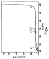
- the graph of Figure 4 shows the numerical simulations of the breakdown voltage for the 6.5 kV ALET of Figure 1 with (a) no termination, (b) p+ surface rings only, (c) equidistant p+ buried layer rings only, and (d) the double layer termination of the invention, namely the p+ buried rings 21 and the p+ surface rings 21.
- the double layer termination technique of the invention leads to much superior breakdown characteristics than either of the known techniques.
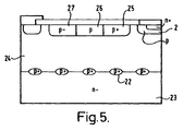
- Figure 5 shows a modified form of the structure of Figure 1, wherein the first voltage termination layer is made of several (at least two) conductive regions (25, 26, 27) such that the region 25 closest to the active area is highly doped; and, as the distance from the active area increases, the doping of these regions 26, 27 decreases.
- the purpose of the second voltage termination layer is to act as a first filter for the potential lines, whilst the first voltage termination layer, comprising the above-mentioned regions 25,26, 27, provides even distribution of the potential lines at the device surface.
- at least one of the p type regions 25, 26, 27 is formed at the same time, and/or uses the same mask, as that used to form the p-base region 2.
- edge termination structure described above in connection with an ALET could be used with other power semiconductor devices, and in particular to a large class of high to ultra-high voltage devices such as diodes, DMOSFETs DMOS IGBTs, trench MOSFETS and trench IGBTs.
Landscapes
- Metal-Oxide And Bipolar Metal-Oxide Semiconductor Integrated Circuits (AREA)
- Element Separation (AREA)
- Thyristors (AREA)
Applications Claiming Priority (2)
| Application Number | Priority Date | Filing Date | Title |
|---|---|---|---|
| GB9918980 | 1999-08-11 | ||
| GB9918980A GB2354879B (en) | 1999-08-11 | 1999-08-11 | A semiconductor device |
Publications (2)
| Publication Number | Publication Date |
|---|---|
| EP1076364A2 true EP1076364A2 (de) | 2001-02-14 |
| EP1076364A3 EP1076364A3 (de) | 2003-07-30 |
Family
ID=10858992
Family Applications (1)
| Application Number | Title | Priority Date | Filing Date |
|---|---|---|---|
| EP00306256A Withdrawn EP1076364A3 (de) | 1999-08-11 | 2000-07-24 | Leistungshalbleiteranordnung |
Country Status (3)
| Country | Link |
|---|---|
| US (1) | US6426520B1 (de) |
| EP (1) | EP1076364A3 (de) |
| GB (1) | GB2354879B (de) |
Cited By (5)
| Publication number | Priority date | Publication date | Assignee | Title |
|---|---|---|---|---|
| DE10240107A1 (de) * | 2002-08-30 | 2004-03-11 | Infineon Technologies Ag | Randabschluss für Leistungshalbleiterbauelement, Verfahren zu dessen Herstellung und mit dem Verfahren hergestellte Diode |
| US8110888B2 (en) | 2007-09-18 | 2012-02-07 | Microsemi Corporation | Edge termination for high voltage semiconductor device |
| WO2015044738A1 (en) * | 2013-09-24 | 2015-04-02 | Toyota Jidosha Kabushiki Kaisha | Semiconductor device |
| CN110854072A (zh) * | 2020-01-07 | 2020-02-28 | 四川立泰电子有限公司 | 低电磁干扰功率器件终端结构的制造工艺 |
| EP4435864A4 (de) * | 2021-12-27 | 2025-03-19 | Nanjing Sinnopower Technology Co., Ltd. | Halbleiteranordnung vom stromschutztyp |
Families Citing this family (10)
| Publication number | Priority date | Publication date | Assignee | Title |
|---|---|---|---|---|
| US7037814B1 (en) * | 2003-10-10 | 2006-05-02 | National Semiconductor Corporation | Single mask control of doping levels |
| US8154078B2 (en) * | 2010-02-17 | 2012-04-10 | Vanguard International Semiconductor Corporation | Semiconductor structure and fabrication method thereof |
| US9716167B2 (en) * | 2011-02-22 | 2017-07-25 | National Semiconductor Corporation | Trench DMOS transistor with reduced gate-to-drain capacitance |
| JP6139356B2 (ja) * | 2013-09-24 | 2017-05-31 | トヨタ自動車株式会社 | 半導体装置 |
| JP7092129B2 (ja) | 2017-07-04 | 2022-06-28 | 住友電気工業株式会社 | 炭化珪素半導体装置 |
| CN107316816B (zh) * | 2017-07-12 | 2020-06-16 | 广州粤芯半导体技术有限公司 | 一种沟槽型功率器件及其制作方法 |
| JP6648331B1 (ja) * | 2019-06-07 | 2020-02-14 | 新電元工業株式会社 | 半導体装置及び半導体装置の製造方法 |
| CN110556427B (zh) * | 2019-08-07 | 2021-01-08 | 南京芯舟科技有限公司 | 半导体器件及其结边缘区 |
| WO2021111528A1 (ja) * | 2019-12-03 | 2021-06-10 | トヨタ自動車株式会社 | 半導体装置 |
| JP7722177B2 (ja) * | 2021-12-24 | 2025-08-13 | 株式会社デンソー | 半導体装置 |
Family Cites Families (12)
| Publication number | Priority date | Publication date | Assignee | Title |
|---|---|---|---|---|
| US4003072A (en) * | 1972-04-20 | 1977-01-11 | Sony Corporation | Semiconductor device with high voltage breakdown resistance |
| JPS523277B2 (de) * | 1973-05-19 | 1977-01-27 | ||
| GB1558506A (en) * | 1976-08-09 | 1980-01-03 | Mullard Ltd | Semiconductor devices having a rectifying metalto-semicondductor junction |
| US4267557A (en) * | 1978-06-08 | 1981-05-12 | Tokyo Shibaura Denki Kabushiki Kaisha | Semiconductor device |
| US4329705A (en) * | 1979-05-21 | 1982-05-11 | Exxon Research & Engineering Co. | VMOS/Bipolar power switching device |
| SE427598B (sv) * | 1981-08-25 | 1983-04-18 | Ericsson Telefon Ab L M | Halvledardiod avsedd att inga i integrerade kretsar |
| GB2193596A (en) * | 1986-08-08 | 1988-02-10 | Philips Electronic Associated | A semiconductor diode |
| DE69029180T2 (de) * | 1989-08-30 | 1997-05-22 | Siliconix Inc | Transistor mit Spannungsbegrenzungsanordnung |
| JP2601143B2 (ja) * | 1993-06-17 | 1997-04-16 | 日本電気株式会社 | 半導体装置 |
| JPH0878661A (ja) * | 1994-09-08 | 1996-03-22 | Meidensha Corp | 電力用半導体素子 |
| DE69531783T2 (de) * | 1995-10-09 | 2004-07-15 | Consorzio Per La Ricerca Sulla Microelettronica Nel Mezzogiorno - Corimme | Herstellungsverfahren für Leistungsanordnung mit Schutzring |
| GB2327295A (en) * | 1997-07-11 | 1999-01-20 | Plessey Semiconductors Ltd | MOS controllable power semiconductor device |
-
1999
- 1999-08-11 GB GB9918980A patent/GB2354879B/en not_active Expired - Fee Related
-
2000
- 2000-07-24 EP EP00306256A patent/EP1076364A3/de not_active Withdrawn
- 2000-08-10 US US09/636,111 patent/US6426520B1/en not_active Expired - Fee Related
Cited By (6)
| Publication number | Priority date | Publication date | Assignee | Title |
|---|---|---|---|---|
| DE10240107A1 (de) * | 2002-08-30 | 2004-03-11 | Infineon Technologies Ag | Randabschluss für Leistungshalbleiterbauelement, Verfahren zu dessen Herstellung und mit dem Verfahren hergestellte Diode |
| DE10240107B4 (de) * | 2002-08-30 | 2008-03-06 | Infineon Technologies Ag | Randabschluss für Leistungshalbleiterbauelement und für Diode sowie Verfahren zur Herstellung einer n-leitenden Zone für einen solchen Randabschluss |
| US8110888B2 (en) | 2007-09-18 | 2012-02-07 | Microsemi Corporation | Edge termination for high voltage semiconductor device |
| WO2015044738A1 (en) * | 2013-09-24 | 2015-04-02 | Toyota Jidosha Kabushiki Kaisha | Semiconductor device |
| CN110854072A (zh) * | 2020-01-07 | 2020-02-28 | 四川立泰电子有限公司 | 低电磁干扰功率器件终端结构的制造工艺 |
| EP4435864A4 (de) * | 2021-12-27 | 2025-03-19 | Nanjing Sinnopower Technology Co., Ltd. | Halbleiteranordnung vom stromschutztyp |
Also Published As
| Publication number | Publication date |
|---|---|
| US6426520B1 (en) | 2002-07-30 |
| GB9918980D0 (en) | 1999-10-13 |
| GB2354879B (en) | 2004-05-12 |
| EP1076364A3 (de) | 2003-07-30 |
| GB2354879A (en) | 2001-04-04 |
Similar Documents
| Publication | Publication Date | Title |
|---|---|---|
| JP7182594B2 (ja) | ゲート・トレンチと、埋め込まれた終端構造とを有するパワー半導体デバイス、及び、関連方法 | |
| JP7550239B2 (ja) | セグメント化されたトレンチとシールドとを伴うトレンチ型パワー・デバイス | |
| US10396158B2 (en) | Termination structure for nanotube semiconductor devices | |
| US9093522B1 (en) | Vertical power MOSFET with planar channel and vertical field plate | |
| US6239463B1 (en) | Low resistance power MOSFET or other device containing silicon-germanium layer | |
| EP0746030B1 (de) | Grabengate-Leistungs-MOSFET mit Schutzdioden in periodischer Anordnung | |
| US11195941B2 (en) | Semiconductor device | |
| US7723783B2 (en) | Semiconductor device | |
| US6359308B1 (en) | Cellular trench-gate field-effect transistors | |
| US7910486B2 (en) | Method for forming nanotube semiconductor devices | |
| KR101660935B1 (ko) | 증가된 항복 전압 특성을 갖는 트렌치형 전력 반도체 소자 | |
| CN1248298C (zh) | 制造半导体整流器件的方法及所得器件 | |
| JP2023065461A (ja) | 半導体装置 | |
| US12009389B2 (en) | Edge termination for power semiconductor devices and related fabrication methods | |
| US20060216896A1 (en) | Semiconductor device and method for manufacturing same | |
| US6426520B1 (en) | Semiconductor device | |
| CN107112356A (zh) | 具有薄底部射极层并在屏蔽区域和终止环中的渠沟中植入掺杂物的垂直功率电晶体 | |
| US20060220156A1 (en) | Semiconductor device and method for manufacturing same | |
| EP3012870A1 (de) | Randabschluss für Hochspannungs-Halbleitervorrichtungen | |
| US12034001B2 (en) | Concept for silicon carbide power devices | |
| US6768170B2 (en) | Superjunction device with improved avalanche capability and breakdown voltage | |
| US20250194134A1 (en) | Mos-gated trench device having shallow gate trenches and deep isolation trenches | |
| WO1998005075A2 (en) | Semiconductor component with linear current-to-voltage characteristics | |
| JP3998454B2 (ja) | 電力用半導体装置 | |
| US5959345A (en) | Edge termination for zener-clamped power device |
Legal Events
| Date | Code | Title | Description |
|---|---|---|---|
| PUAI | Public reference made under article 153(3) epc to a published international application that has entered the european phase |
Free format text: ORIGINAL CODE: 0009012 |
|
| AK | Designated contracting states |
Kind code of ref document: A2 Designated state(s): AT BE CH CY DE DK ES FI FR GB GR IE IT LI LU MC NL PT SE |
|
| AX | Request for extension of the european patent |
Free format text: AL;LT;LV;MK;RO;SI |
|
| PUAL | Search report despatched |
Free format text: ORIGINAL CODE: 0009013 |
|
| AK | Designated contracting states |
Designated state(s): AT BE CH CY DE DK ES FI FR GB GR IE IT LI LU MC NL PT SE |
|
| AX | Request for extension of the european patent |
Extension state: AL LT LV MK RO SI |
|
| 17P | Request for examination filed |
Effective date: 20040129 |
|
| AKX | Designation fees paid |
Designated state(s): DE FR GB |
|
| 17Q | First examination report despatched |
Effective date: 20041028 |
|
| STAA | Information on the status of an ep patent application or granted ep patent |
Free format text: STATUS: THE APPLICATION IS DEEMED TO BE WITHDRAWN |
|
| 18D | Application deemed to be withdrawn |
Effective date: 20050408 |