EP1076406B1 - Onduleur demi-pont - Google Patents
Onduleur demi-pont Download PDFInfo
- Publication number
- EP1076406B1 EP1076406B1 EP00116151A EP00116151A EP1076406B1 EP 1076406 B1 EP1076406 B1 EP 1076406B1 EP 00116151 A EP00116151 A EP 00116151A EP 00116151 A EP00116151 A EP 00116151A EP 1076406 B1 EP1076406 B1 EP 1076406B1
- Authority
- EP
- European Patent Office
- Prior art keywords
- bridge inverter
- parallel
- switch
- capacitor
- inductor
- Prior art date
- Legal status (The legal status is an assumption and is not a legal conclusion. Google has not performed a legal analysis and makes no representation as to the accuracy of the status listed.)
- Expired - Lifetime
Links
- 239000003990 capacitor Substances 0.000 claims abstract description 46
- 230000008878 coupling Effects 0.000 claims abstract description 24
- 238000010168 coupling process Methods 0.000 claims abstract description 24
- 238000005859 coupling reaction Methods 0.000 claims abstract description 24
- 230000003068 static effect Effects 0.000 abstract 2
- 238000009499 grossing Methods 0.000 description 4
- 230000001629 suppression Effects 0.000 description 3
- 230000000694 effects Effects 0.000 description 2
- 230000005415 magnetization Effects 0.000 description 2
- RYGMFSIKBFXOCR-UHFFFAOYSA-N Copper Chemical compound [Cu] RYGMFSIKBFXOCR-UHFFFAOYSA-N 0.000 description 1
- 229910052802 copper Inorganic materials 0.000 description 1
- 239000010949 copper Substances 0.000 description 1
- 230000001419 dependent effect Effects 0.000 description 1
Images

Classifications
-
- H—ELECTRICITY
- H02—GENERATION; CONVERSION OR DISTRIBUTION OF ELECTRIC POWER
- H02M—APPARATUS FOR CONVERSION BETWEEN AC AND AC, BETWEEN AC AND DC, OR BETWEEN DC AND DC, AND FOR USE WITH MAINS OR SIMILAR POWER SUPPLY SYSTEMS; CONVERSION OF DC OR AC INPUT POWER INTO SURGE OUTPUT POWER; CONTROL OR REGULATION THEREOF
- H02M7/00—Conversion of AC power input into DC power output; Conversion of DC power input into AC power output
- H02M7/42—Conversion of DC power input into AC power output without possibility of reversal
- H02M7/44—Conversion of DC power input into AC power output without possibility of reversal by static converters
- H02M7/48—Conversion of DC power input into AC power output without possibility of reversal by static converters using discharge tubes with control electrode or semiconductor devices with control electrode
- H02M7/53—Conversion of DC power input into AC power output without possibility of reversal by static converters using discharge tubes with control electrode or semiconductor devices with control electrode using devices of a triode or transistor type requiring continuous application of a control signal
- H02M7/537—Conversion of DC power input into AC power output without possibility of reversal by static converters using discharge tubes with control electrode or semiconductor devices with control electrode using devices of a triode or transistor type requiring continuous application of a control signal using semiconductor devices only, e.g. single switched pulse inverters
- H02M7/538—Conversion of DC power input into AC power output without possibility of reversal by static converters using discharge tubes with control electrode or semiconductor devices with control electrode using devices of a triode or transistor type requiring continuous application of a control signal using semiconductor devices only, e.g. single switched pulse inverters in a push-pull configuration
Definitions
- the present invention relates to a half-bridge inverter according to the preamble of claim 1.
- FIG. 1 Such a known from the prior art half-bridge inverter (see DE-A 197 22 124) is shown in Fig. 1.
- a first and a second input terminal E, N form an input to which a storage capacitor C3 is connected in parallel.
- Parallel to the storage capacitor C3 is located as a surge arrester on the one hand, a varistor, i. a non-linear resistor, which ensures in practice the required surge resistance, further the series connection of a first and a second coupling capacitor C1, C2, whose center is connected to the first output terminal B of the half-bridge inverter.
- the coupling capacitors C1, C2 in this case form the passive bridge branch of the half-bridge inverter.
- the active bridge branch of the half-bridge inverter comprising a first switch S1 and a second switch S2, is connected at its center via an inductance L1 to the second output terminal A of the half-bridge inverter, wherein the inductance L1 acts as Umschwinginduktterrorism.
- the push-pull operated switches S1 and S2 are each a freewheeling diode D1, D2 and a Umschwingkondensator CS1, CS2 connected in parallel.
- a disadvantage of the half-bridge inverter shown in FIG. 1 is, on the one hand, that the AC flowing through C3 is indeed filtered off by C3, but this is not sufficient in practice, so that undesirable effects on the Entrance E, N is coming.
- the circuit for providing a high-frequency AC voltage at the terminals B A dimensioned result problems with radio interference suppression.
- the inductance L1 carries both the current and the magnetization load. As a result, the inductance L1 must be large, resulting in an undesirably large amount of space.
- the object of the present invention is therefore to eliminate these disadvantages, in particular to provide a half-bridge inverter, which can be realized with a smaller design.
- the half-bridge inverter according to the invention has the advantage that the current and magnetization load is divided into two inductors.
- the current load of each inductance L1, L2 is therefore halved compared to the current load of the inductance L1 according to FIG.
- the copper losses are thus only a quarter. This allows realization by smaller components and thus reduces the space requirement on a circuit board. In particular, at higher powers, thereby facilitating the realization considerably.
- the storage capacitor C3 is advantageously no longer arranged between the input terminals E, N in the subject invention, but is located at the other end of the circuit, so to speak.
- the filter order increases particularly advantageously by two orders, as seen from the input E, N. This leads to a significant improvement of the radio interference suppression as well as to an increase in the Surge resistance, provided that a surge arrester is connected in parallel with C3.
- the filter to be provided in a preliminary stage to the left of the input E, N in FIG. 2 can therefore be made simpler.
- first switch a first freewheeling diode and the second switch a second freewheeling diode in parallel. Furthermore, it can be provided that a first Umschwingkondensator is arranged parallel to the first switch and / or a second Umschwingkondensator parallel to the second switch.
- the optional surge arrester VAR can be realized as a nonlinear resistor, in particular as a varistor.
- the capacitance value of the first coupling capacitor can, in a particularly advantageous manner, be substantially equal to the capacitance value of the second coupling capacitor.
- the capacitance value of the storage capacitor which acts as a back-up capacitor for the active bridge branch in the half-bridge inverter according to the invention, is preferably twice the capacitance value of the first and / or the second coupling capacitor.
- the first inductor is coupled to the second inductor.
- the coupling can also be carried out so that the main inductances of the first and the second inductance lead to a smoothing of the input current and that the leakage inductances of the first and the second inductance act as Umschwingindukt ceremonies.
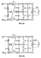
- FIG. 2 a shows a first embodiment of a half-bridge inverter according to the invention, the passive bridge branch formed by the coupling capacitors C 1, C 2 being arranged parallel to the input terminals E, N.
- the center of the passive bridge branch is connected to the output terminal B.
- the active bridge branch comprises two switches S1, S2 connected in series whose center is connected to the second output terminal A. Parallel to each switch, a respective freewheeling diode D1, D2, and a respective Umschwingkondensator CS1, CS2 is arranged.
- a storage capacitor C3 is connected in parallel to the active bridge branch.
- an optional surge arrester VAR is shown in FIG. 2a.
- the coupling capacitor C2 is connected to the switch S2 via an inductance L2, while the coupling capacitor C1 is connected to the switch S1 via an inductance L1.
- Dashed line shows the course of the DC current from the input terminal E via the inductance L2, the storage capacitor C3 (in these considerations, the resistance of the surge arrester can be assumed to be infinite.
- the curves of the two alternating current components are shown in dashed lines, wherein in Fig. 2a, the switch S2 is closed, a first AC component flows from the output terminal B through the coupling capacitor C2 via the inductor L2 through the switch S2 to the second output terminal A.
- the second AC component flows from the output terminal B via the coupling capacitor C1, through the inductance L1, the storage capacitor C3 and the closed switch S2 to the second output terminal A.
- Fig. 2b shows the conditions with the switch S1 closed.
- the course of the direct current is unchanged.
- a first one passes from the output terminal A through the switch S1, through the inductor L1, through the coupling capacitor C1 to the output terminal B, while a second portion from the output terminal A, through the switch S1, the storage capacitor C3, the inductance L2, Coupling capacitor C2 to the output terminal B flows.
- From the current balance at C3 shows that the storage capacitor is charged by the DC, while the respective AC component discharges the storage capacitor C3.
- A acts as a Umschwinginduktterrorism the parallel connection of the inductors L1, L2.
- the load is thus distributed over the two inductors L1 and L2.
- the with respect to the input terminals E, N serially acting inductors L1, L2 lead to an effective smoothing of the input current.
- AC components are only screened out by the capacitor C3.
- Fig. 3a, 3b show a further embodiment of the half-bridge inverter according to the invention.
- 3a shows the DC and AC curves with the switch S2 closed
- FIG. 3b with the switch S1 closed, these corresponding to those of FIGS. 2a and 2b.
- the two inductances L1, L2 are coupled together. This will cause the smoothing effect significantly increased on the input current.
- the main inductances of the two inductors L1, L2 lead to a smoothing of the input current, while the leakage inductances of the two inductors L1, L2 act as a Umschwinginduktterrorism.
- a realization in which both inductors L1, L2 are wound on a single core is possible.
- the filter arrangement is increased by 2 orders - as seen from the input E, N - in the half-bridge inverters according to the invention. This leads to a significant improvement of the radio interference suppression and to an increase in the surge resistance, provided that a surge arrester VAR is connected in parallel with the storage capacitor C3.
Landscapes
- Engineering & Computer Science (AREA)
- Power Engineering (AREA)
- Inverter Devices (AREA)
- Control Of Motors That Do Not Use Commutators (AREA)
Claims (9)
- Onduleur à demi-pont comprenant :une première et une deuxième bornes (E, N)d'entrée, qui forment une entrée de l'onduleur à demi-pont ;une première et une deuxième bornes (B, A) de sortie, qui forment une sortie de l'onduleur à demi-pont ;un circuit série constitué d'un premier et d'un deuxième condensateurs (C1, C2) de couplage, qui est monté en parallèle à l'entrée et qui forme une branche passive du pont, un point médian du circuit série constitué du premier et du deuxième condensateurs (C1, C2) de couplage étant reliés à la première borne (B) de sortie ;un circuit série constitué d'un premier et d'un deuxième interrupteurs (S1, S2), qui forme une branche active du pont et dont le point médian est relié à la deuxième borne (A) de sortie, l'onduleur à demi-pont comprenant une inductance d'oscillation,
caractérisé
en ce qu'un condensateur (C3) d'emmagasinage est monté parallèlement à la branche active du pont et le premier condensateur (C1) de couplage est relié directement par une première inductance (L1) et le deuxième condensateur (C2) de couplage par une deuxième inductance (L2) au condensateur (C3) d'emmagasinage, la première et la deuxième inductances formant les composants uniques de l'inductance d'oscillation. - Onduleur à demi-pont suivant la revendication 1,
caractérisé
en ce qu'une première diode (D1) de roue libre est montée en parallèle au premier interrupteur (S1) et une deuxième diode (D2) de roue libre est montée en parallèle au deuxième interrupteur. - Onduleur à demi-pont suivant la revendication 1 ou 2,
caractérisé
en ce qu'un premier condensateur (CS1) d'oscillation est monté en parallèle au premier interrupteur (S1) et/ou un deuxième condensateur (CS2) d'oscillation est monté en parallèle au deuxième interrupteur (S2). - Onduleur à demi-pont suivant l'une des revendications précédentes,
caractérisé
en ce qu'une résistance (VAR) non linéaire est montée en tant que limiteur de tension en parallèle au condensateur (C3) d'emmagasinage. - Onduleur à demi-pont suivant l'une des revendications précédentes,
caractérisé
en ce que la capacité du premier condensateur (C1) de couplage est sensiblement égale à la capacité du deuxième condensateur (C2) de couplage. - Onduleur à demi-pont suivant l'une des revendications précédentes,
caractérisé
en ce que la capacité du condensateur (C3) d'emmagasinage est égale sensiblement au double de la capacité du premier et/ou du deuxième condensateur(s) (C1, C2) de couplage. - Onduleur à demi-pont suivant l'une des revendications précédentes,
caractérisé
en ce que la première inductance (L1) est couplée à la deuxième inductance (L2). - Onduleur à demi-pont suivant la revendication 7,
caractérisé
en ce que la première et la deuxième inductances (L1, L2) sont enroulées sur un noyau unique. - Onduleur à demi-pont suivant la revendication 7 ou 8,
caractérisé
en ce que le couplage est tel que les inductances principales des première et deuxième inductances (L1, L2) entraînent un lissage du courant d'entrée et que les inductances de fuite de la première et de la deuxième inductances (L1, L2) servent d'inductances d'oscillation.
Applications Claiming Priority (2)
| Application Number | Priority Date | Filing Date | Title |
|---|---|---|---|
| DE19937925A DE19937925A1 (de) | 1999-08-11 | 1999-08-11 | Halbbrückenwechselrichter |
| DE19937925 | 1999-08-11 |
Publications (3)
| Publication Number | Publication Date |
|---|---|
| EP1076406A2 EP1076406A2 (fr) | 2001-02-14 |
| EP1076406A3 EP1076406A3 (fr) | 2003-04-23 |
| EP1076406B1 true EP1076406B1 (fr) | 2006-03-01 |
Family
ID=7917973
Family Applications (1)
| Application Number | Title | Priority Date | Filing Date |
|---|---|---|---|
| EP00116151A Expired - Lifetime EP1076406B1 (fr) | 1999-08-11 | 2000-08-01 | Onduleur demi-pont |
Country Status (6)
| Country | Link |
|---|---|
| US (1) | US6266259B1 (fr) |
| EP (1) | EP1076406B1 (fr) |
| JP (1) | JP2001069766A (fr) |
| AT (1) | ATE319218T1 (fr) |
| CA (1) | CA2315445C (fr) |
| DE (2) | DE19937925A1 (fr) |
Families Citing this family (7)
| Publication number | Priority date | Publication date | Assignee | Title |
|---|---|---|---|---|
| US6266659B1 (en) * | 1997-08-07 | 2001-07-24 | Uday P. Nadkarni | Skills database management system and method |
| DE10160790A1 (de) * | 2001-01-12 | 2002-08-08 | Patent Treuhand Ges Fuer Elektrische Gluehlampen Mbh | Schaltungsanordnung zum Einschalten einer Teilschaltungsanordnung |
| US7804281B2 (en) * | 2006-09-13 | 2010-09-28 | Virginia Tech Intellectual Properties, Inc. | Reducing common mode noise of power factor correction converters using general balance concept |
| WO2009030275A1 (fr) * | 2007-09-05 | 2009-03-12 | Abb Technology Ag | Convertisseur de source de tension pour transmission de puissance en courant continu haute tension |
| WO2009068698A1 (fr) * | 2007-11-30 | 2009-06-04 | Ingeteam Energy, S.A. | Circuit électrique de conversion de courant continu en courant alternatif |
| JP5565436B2 (ja) * | 2012-06-27 | 2014-08-06 | 株式会社デンソー | 昇圧装置 |
| US9531292B2 (en) * | 2013-06-14 | 2016-12-27 | Abb Technology Ltd | Arrangement, method and computer program product concerned with tapping of power from a DC power line to an AC power line |
Family Cites Families (8)
| Publication number | Priority date | Publication date | Assignee | Title |
|---|---|---|---|---|
| US4914558A (en) * | 1989-03-06 | 1990-04-03 | Jon Flickinger | Series resonant inverter and method of lamp starting |
| JP2929635B2 (ja) * | 1990-01-31 | 1999-08-03 | 東芝ライテック株式会社 | 電源回路 |
| DE69118501T2 (de) * | 1990-12-25 | 1996-09-26 | Matsushita Electric Works Ltd | Wechselrichteranordnung |
| JP3250222B2 (ja) * | 1990-12-25 | 2002-01-28 | 松下電工株式会社 | インバータ装置 |
| US5502635A (en) * | 1993-01-19 | 1996-03-26 | Andrzej A. Bobel | Parallel resonant integrated inverter ballast for gas discharge lamps |
| US5875103A (en) * | 1995-12-22 | 1999-02-23 | Electronic Measurements, Inc. | Full range soft-switching DC-DC converter |
| US5703438A (en) * | 1996-01-22 | 1997-12-30 | Valmont Industries, Inc. | Line current filter for less than 10% total harmonic distortion |
| DE19722124A1 (de) * | 1997-05-27 | 1998-12-03 | Patent Treuhand Ges Fuer Elektrische Gluehlampen Mbh | Schaltungsanordnung zum Betreiben elektrischer Glühlampen |
-
1999
- 1999-08-11 DE DE19937925A patent/DE19937925A1/de not_active Withdrawn
-
2000
- 2000-08-01 EP EP00116151A patent/EP1076406B1/fr not_active Expired - Lifetime
- 2000-08-01 DE DE50012276T patent/DE50012276D1/de not_active Expired - Lifetime
- 2000-08-01 AT AT00116151T patent/ATE319218T1/de not_active IP Right Cessation
- 2000-08-07 JP JP2000238966A patent/JP2001069766A/ja active Pending
- 2000-08-09 US US09/635,209 patent/US6266259B1/en not_active Expired - Lifetime
- 2000-08-10 CA CA002315445A patent/CA2315445C/fr not_active Expired - Fee Related
Also Published As
| Publication number | Publication date |
|---|---|
| US6266259B1 (en) | 2001-07-24 |
| CA2315445A1 (fr) | 2001-02-11 |
| DE19937925A1 (de) | 2001-02-15 |
| EP1076406A2 (fr) | 2001-02-14 |
| DE50012276D1 (de) | 2006-04-27 |
| EP1076406A3 (fr) | 2003-04-23 |
| JP2001069766A (ja) | 2001-03-16 |
| ATE319218T1 (de) | 2006-03-15 |
| CA2315445C (fr) | 2008-12-09 |
Similar Documents
| Publication | Publication Date | Title |
|---|---|---|
| DE3325612C2 (fr) | ||
| DE3333768C2 (fr) | ||
| EP0352703B1 (fr) | Ballast électronique | |
| EP0899859B1 (fr) | Onduleur avec circuit intermédiaire de tension | |
| DE2950411A1 (de) | Gleichrichtervorrichtung mit gesiebter ausgangsspannung | |
| EP3460978A1 (fr) | Agencement de circuit électrique destiné au circuit de protection d'entrée d'un convertisseur continu-continu et convertisseur continu-continu | |
| DE19700100C2 (de) | Tiefsetzsteller | |
| EP1076406B1 (fr) | Onduleur demi-pont | |
| DE19537155A1 (de) | Spannungsteiler für Hochspannungen | |
| EP0808085B1 (fr) | Alimentation à haute fréquence pour une lampe à décharge basse pression avec une compatibilité électromagnétique accrue | |
| DE4030193C2 (de) | Netzfilter | |
| DE10310577A1 (de) | Nullspannungsfilter für Umrichter mit selbstgeführtem Netzstromrichter (AFE) und Gleichspannungszwischenkreis | |
| EP0239786B1 (fr) | Réactance pour un dispositif de commutation haute puissance | |
| EP1076405B1 (fr) | Redresseur avec alimentation au point milieu | |
| DE10138751B4 (de) | Wechselrichter mit schnellschaltenden ansteuerbaren elektronischen Schaltern, insbesondere IGBT-Schaltern, sowie Verfahren zur Ansteuerung eines derartigen Wechselrichters | |
| EP4214813A1 (fr) | Dispositif de commande | |
| EP1318594B1 (fr) | Circuit convertisseur de puissance pour augmentation d'une tension alternative | |
| DE102018010146A1 (de) | Vorrichtung zur Filterung von hochfrequenten Störspannungen in einer Schaltung zur Leistungsfaktorkorrektur | |
| DE3635365A1 (de) | Sekundaerseitig schaltbares netzgeraet | |
| DE2838062A1 (de) | Anordnung mit parallel geschalteten gleichstrom-umrichtern | |
| DE4039874A1 (de) | Leitungsfilter | |
| DE3342011C2 (de) | Tiefpaßfilter für elektrische Verbraucher | |
| EP3769410A1 (fr) | Ensemble filtre emv | |
| DE2718598A1 (de) | Stoerstromreduzierende stromrichterbeschaltung | |
| DE3310558A1 (de) | Wechselrichter mit thyristoren |
Legal Events
| Date | Code | Title | Description |
|---|---|---|---|
| PUAI | Public reference made under article 153(3) epc to a published international application that has entered the european phase |
Free format text: ORIGINAL CODE: 0009012 |
|
| AK | Designated contracting states |
Kind code of ref document: A2 Designated state(s): AT BE CH CY DE DK ES FI FR GB GR IE IT LI LU MC NL PT SE |
|
| AX | Request for extension of the european patent |
Free format text: AL;LT;LV;MK;RO;SI |
|
| PUAL | Search report despatched |
Free format text: ORIGINAL CODE: 0009013 |
|
| AK | Designated contracting states |
Designated state(s): AT BE CH CY DE DK ES FI FR GB GR IE IT LI LU MC NL PT SE |
|
| AX | Request for extension of the european patent |
Extension state: AL LT LV MK RO SI |
|
| 17P | Request for examination filed |
Effective date: 20030519 |
|
| AKX | Designation fees paid |
Designated state(s): AT BE CH CY DE DK ES FI FR GB GR IE IT LI LU MC NL PT SE |
|
| 17Q | First examination report despatched |
Effective date: 20031009 |
|
| GRAP | Despatch of communication of intention to grant a patent |
Free format text: ORIGINAL CODE: EPIDOSNIGR1 |
|
| GRAS | Grant fee paid |
Free format text: ORIGINAL CODE: EPIDOSNIGR3 |
|
| GRAA | (expected) grant |
Free format text: ORIGINAL CODE: 0009210 |
|
| AK | Designated contracting states |
Kind code of ref document: B1 Designated state(s): AT BE CH CY DE DK ES FI FR GB GR IE IT LI LU MC NL PT SE |
|
| PG25 | Lapsed in a contracting state [announced via postgrant information from national office to epo] |
Ref country code: IE Free format text: LAPSE BECAUSE OF FAILURE TO SUBMIT A TRANSLATION OF THE DESCRIPTION OR TO PAY THE FEE WITHIN THE PRESCRIBED TIME-LIMIT Effective date: 20060301 Ref country code: FI Free format text: LAPSE BECAUSE OF FAILURE TO SUBMIT A TRANSLATION OF THE DESCRIPTION OR TO PAY THE FEE WITHIN THE PRESCRIBED TIME-LIMIT Effective date: 20060301 |
|
| REG | Reference to a national code |
Ref country code: GB Ref legal event code: FG4D Free format text: NOT ENGLISH |
|
| REG | Reference to a national code |
Ref country code: CH Ref legal event code: EP |
|
| REG | Reference to a national code |
Ref country code: IE Ref legal event code: FG4D Free format text: LANGUAGE OF EP DOCUMENT: GERMAN |
|
| REF | Corresponds to: |
Ref document number: 50012276 Country of ref document: DE Date of ref document: 20060427 Kind code of ref document: P |
|
| GBT | Gb: translation of ep patent filed (gb section 77(6)(a)/1977) |
Effective date: 20060426 |
|
| PG25 | Lapsed in a contracting state [announced via postgrant information from national office to epo] |
Ref country code: DK Free format text: LAPSE BECAUSE OF FAILURE TO SUBMIT A TRANSLATION OF THE DESCRIPTION OR TO PAY THE FEE WITHIN THE PRESCRIBED TIME-LIMIT Effective date: 20060601 |
|
| PG25 | Lapsed in a contracting state [announced via postgrant information from national office to epo] |
Ref country code: ES Free format text: LAPSE BECAUSE OF FAILURE TO SUBMIT A TRANSLATION OF THE DESCRIPTION OR TO PAY THE FEE WITHIN THE PRESCRIBED TIME-LIMIT Effective date: 20060612 |
|
| REG | Reference to a national code |
Ref country code: SE Ref legal event code: TRGR |
|
| PG25 | Lapsed in a contracting state [announced via postgrant information from national office to epo] |
Ref country code: PT Free format text: LAPSE BECAUSE OF FAILURE TO SUBMIT A TRANSLATION OF THE DESCRIPTION OR TO PAY THE FEE WITHIN THE PRESCRIBED TIME-LIMIT Effective date: 20060801 |
|
| PG25 | Lapsed in a contracting state [announced via postgrant information from national office to epo] |
Ref country code: MC Free format text: LAPSE BECAUSE OF NON-PAYMENT OF DUE FEES Effective date: 20060831 Ref country code: CH Free format text: LAPSE BECAUSE OF NON-PAYMENT OF DUE FEES Effective date: 20060831 Ref country code: LI Free format text: LAPSE BECAUSE OF NON-PAYMENT OF DUE FEES Effective date: 20060831 |
|
| ET | Fr: translation filed | ||
| REG | Reference to a national code |
Ref country code: IE Ref legal event code: FD4D |
|
| PLBE | No opposition filed within time limit |
Free format text: ORIGINAL CODE: 0009261 |
|
| STAA | Information on the status of an ep patent application or granted ep patent |
Free format text: STATUS: NO OPPOSITION FILED WITHIN TIME LIMIT |
|
| 26N | No opposition filed |
Effective date: 20061204 |
|
| REG | Reference to a national code |
Ref country code: CH Ref legal event code: PL |
|
| PG25 | Lapsed in a contracting state [announced via postgrant information from national office to epo] |
Ref country code: AT Free format text: LAPSE BECAUSE OF NON-PAYMENT OF DUE FEES Effective date: 20060801 |
|
| PG25 | Lapsed in a contracting state [announced via postgrant information from national office to epo] |
Ref country code: GR Free format text: LAPSE BECAUSE OF FAILURE TO SUBMIT A TRANSLATION OF THE DESCRIPTION OR TO PAY THE FEE WITHIN THE PRESCRIBED TIME-LIMIT Effective date: 20060602 |
|
| PG25 | Lapsed in a contracting state [announced via postgrant information from national office to epo] |
Ref country code: LU Free format text: LAPSE BECAUSE OF NON-PAYMENT OF DUE FEES Effective date: 20060801 |
|
| PG25 | Lapsed in a contracting state [announced via postgrant information from national office to epo] |
Ref country code: CY Free format text: LAPSE BECAUSE OF FAILURE TO SUBMIT A TRANSLATION OF THE DESCRIPTION OR TO PAY THE FEE WITHIN THE PRESCRIBED TIME-LIMIT Effective date: 20060301 |
|
| PGFP | Annual fee paid to national office [announced via postgrant information from national office to epo] |
Ref country code: NL Payment date: 20100813 Year of fee payment: 11 |
|
| PGFP | Annual fee paid to national office [announced via postgrant information from national office to epo] |
Ref country code: IT Payment date: 20100825 Year of fee payment: 11 Ref country code: SE Payment date: 20100810 Year of fee payment: 11 |
|
| PGFP | Annual fee paid to national office [announced via postgrant information from national office to epo] |
Ref country code: GB Payment date: 20110811 Year of fee payment: 12 Ref country code: FR Payment date: 20110826 Year of fee payment: 12 |
|
| REG | Reference to a national code |
Ref country code: DE Ref legal event code: R081 Ref document number: 50012276 Country of ref document: DE Owner name: OSRAM GMBH, DE Free format text: FORMER OWNER: OSRAM GESELLSCHAFT MIT BESCHRAENKTER HAFTUNG, 81543 MUENCHEN, DE Effective date: 20111128 |
|
| REG | Reference to a national code |
Ref country code: NL Ref legal event code: V1 Effective date: 20120301 |
|
| REG | Reference to a national code |
Ref country code: SE Ref legal event code: EUG |
|
| PG25 | Lapsed in a contracting state [announced via postgrant information from national office to epo] |
Ref country code: NL Free format text: LAPSE BECAUSE OF NON-PAYMENT OF DUE FEES Effective date: 20120301 Ref country code: IT Free format text: LAPSE BECAUSE OF NON-PAYMENT OF DUE FEES Effective date: 20110801 |
|
| REG | Reference to a national code |
Ref country code: DE Ref legal event code: R081 Ref document number: 50012276 Country of ref document: DE Owner name: OSRAM GMBH, DE Free format text: FORMER OWNER: OSRAM AG, 81543 MUENCHEN, DE Effective date: 20130205 |
|
| GBPC | Gb: european patent ceased through non-payment of renewal fee |
Effective date: 20120801 |
|
| PG25 | Lapsed in a contracting state [announced via postgrant information from national office to epo] |
Ref country code: SE Free format text: LAPSE BECAUSE OF NON-PAYMENT OF DUE FEES Effective date: 20110802 |
|
| REG | Reference to a national code |
Ref country code: FR Ref legal event code: ST Effective date: 20130430 |
|
| PG25 | Lapsed in a contracting state [announced via postgrant information from national office to epo] |
Ref country code: GB Free format text: LAPSE BECAUSE OF NON-PAYMENT OF DUE FEES Effective date: 20120801 |
|
| PG25 | Lapsed in a contracting state [announced via postgrant information from national office to epo] |
Ref country code: FR Free format text: LAPSE BECAUSE OF NON-PAYMENT OF DUE FEES Effective date: 20120831 |
|
| REG | Reference to a national code |
Ref country code: DE Ref legal event code: R081 Ref document number: 50012276 Country of ref document: DE Owner name: OSRAM GMBH, DE Free format text: FORMER OWNER: OSRAM GMBH, 81543 MUENCHEN, DE Effective date: 20130822 |
|
| PGFP | Annual fee paid to national office [announced via postgrant information from national office to epo] |
Ref country code: DE Payment date: 20140821 Year of fee payment: 15 |
|
| PGFP | Annual fee paid to national office [announced via postgrant information from national office to epo] |
Ref country code: BE Payment date: 20140820 Year of fee payment: 15 |
|
| REG | Reference to a national code |
Ref country code: DE Ref legal event code: R119 Ref document number: 50012276 Country of ref document: DE |
|
| PG25 | Lapsed in a contracting state [announced via postgrant information from national office to epo] |
Ref country code: DE Free format text: LAPSE BECAUSE OF NON-PAYMENT OF DUE FEES Effective date: 20160301 |
|
| PG25 | Lapsed in a contracting state [announced via postgrant information from national office to epo] |
Ref country code: BE Free format text: LAPSE BECAUSE OF NON-PAYMENT OF DUE FEES Effective date: 20150831 |