EP1078329B1 - Systemes et procedes assurant la fourniture de puissance en radiofrequence via des boucles de courant en phase et permettant l'identification d'etiquettes d'identification en radiofrequence interrogees simultanement - Google Patents
Systemes et procedes assurant la fourniture de puissance en radiofrequence via des boucles de courant en phase et permettant l'identification d'etiquettes d'identification en radiofrequence interrogees simultanement Download PDFInfo
- Publication number
- EP1078329B1 EP1078329B1 EP99924290A EP99924290A EP1078329B1 EP 1078329 B1 EP1078329 B1 EP 1078329B1 EP 99924290 A EP99924290 A EP 99924290A EP 99924290 A EP99924290 A EP 99924290A EP 1078329 B1 EP1078329 B1 EP 1078329B1
- Authority
- EP
- European Patent Office
- Prior art keywords
- current loops
- phase
- array
- current
- loops
- Prior art date
- Legal status (The legal status is an assumption and is not a legal conclusion. Google has not performed a legal analysis and makes no representation as to the accuracy of the status listed.)
- Expired - Lifetime
Links
Images








Classifications
-
- G—PHYSICS
- G06—COMPUTING OR CALCULATING; COUNTING
- G06K—GRAPHICAL DATA READING; PRESENTATION OF DATA; RECORD CARRIERS; HANDLING RECORD CARRIERS
- G06K7/00—Methods or arrangements for sensing record carriers, e.g. for reading patterns
- G06K7/10—Methods or arrangements for sensing record carriers, e.g. for reading patterns by electromagnetic radiation, e.g. optical sensing; by corpuscular radiation
- G06K7/10009—Methods or arrangements for sensing record carriers, e.g. for reading patterns by electromagnetic radiation, e.g. optical sensing; by corpuscular radiation sensing by radiation using wavelengths larger than 0.1 mm, e.g. radio-waves or microwaves
- G06K7/10316—Methods or arrangements for sensing record carriers, e.g. for reading patterns by electromagnetic radiation, e.g. optical sensing; by corpuscular radiation sensing by radiation using wavelengths larger than 0.1 mm, e.g. radio-waves or microwaves using at least one antenna particularly designed for interrogating the wireless record carriers
- G06K7/10346—Methods or arrangements for sensing record carriers, e.g. for reading patterns by electromagnetic radiation, e.g. optical sensing; by corpuscular radiation sensing by radiation using wavelengths larger than 0.1 mm, e.g. radio-waves or microwaves using at least one antenna particularly designed for interrogating the wireless record carriers the antenna being of the far field type, e.g. HF types or dipoles
-
- G—PHYSICS
- G06—COMPUTING OR CALCULATING; COUNTING
- G06K—GRAPHICAL DATA READING; PRESENTATION OF DATA; RECORD CARRIERS; HANDLING RECORD CARRIERS
- G06K7/00—Methods or arrangements for sensing record carriers, e.g. for reading patterns
- G06K7/0008—General problems related to the reading of electronic memory record carriers, independent of its reading method, e.g. power transfer
-
- G—PHYSICS
- G06—COMPUTING OR CALCULATING; COUNTING
- G06K—GRAPHICAL DATA READING; PRESENTATION OF DATA; RECORD CARRIERS; HANDLING RECORD CARRIERS
- G06K7/00—Methods or arrangements for sensing record carriers, e.g. for reading patterns
- G06K7/10—Methods or arrangements for sensing record carriers, e.g. for reading patterns by electromagnetic radiation, e.g. optical sensing; by corpuscular radiation
- G06K7/10009—Methods or arrangements for sensing record carriers, e.g. for reading patterns by electromagnetic radiation, e.g. optical sensing; by corpuscular radiation sensing by radiation using wavelengths larger than 0.1 mm, e.g. radio-waves or microwaves
- G06K7/10019—Methods or arrangements for sensing record carriers, e.g. for reading patterns by electromagnetic radiation, e.g. optical sensing; by corpuscular radiation sensing by radiation using wavelengths larger than 0.1 mm, e.g. radio-waves or microwaves resolving collision on the communication channels between simultaneously or concurrently interrogated record carriers.
- G06K7/10029—Methods or arrangements for sensing record carriers, e.g. for reading patterns by electromagnetic radiation, e.g. optical sensing; by corpuscular radiation sensing by radiation using wavelengths larger than 0.1 mm, e.g. radio-waves or microwaves resolving collision on the communication channels between simultaneously or concurrently interrogated record carriers. the collision being resolved in the time domain, e.g. using binary tree search or RFID responses allocated to a random time slot
- G06K7/10039—Methods or arrangements for sensing record carriers, e.g. for reading patterns by electromagnetic radiation, e.g. optical sensing; by corpuscular radiation sensing by radiation using wavelengths larger than 0.1 mm, e.g. radio-waves or microwaves resolving collision on the communication channels between simultaneously or concurrently interrogated record carriers. the collision being resolved in the time domain, e.g. using binary tree search or RFID responses allocated to a random time slot interrogator driven, i.e. synchronous
-
- G—PHYSICS
- G06—COMPUTING OR CALCULATING; COUNTING
- G06K—GRAPHICAL DATA READING; PRESENTATION OF DATA; RECORD CARRIERS; HANDLING RECORD CARRIERS
- G06K7/00—Methods or arrangements for sensing record carriers, e.g. for reading patterns
- G06K7/10—Methods or arrangements for sensing record carriers, e.g. for reading patterns by electromagnetic radiation, e.g. optical sensing; by corpuscular radiation
- G06K7/10009—Methods or arrangements for sensing record carriers, e.g. for reading patterns by electromagnetic radiation, e.g. optical sensing; by corpuscular radiation sensing by radiation using wavelengths larger than 0.1 mm, e.g. radio-waves or microwaves
- G06K7/10316—Methods or arrangements for sensing record carriers, e.g. for reading patterns by electromagnetic radiation, e.g. optical sensing; by corpuscular radiation sensing by radiation using wavelengths larger than 0.1 mm, e.g. radio-waves or microwaves using at least one antenna particularly designed for interrogating the wireless record carriers
-
- G—PHYSICS
- G06—COMPUTING OR CALCULATING; COUNTING
- G06K—GRAPHICAL DATA READING; PRESENTATION OF DATA; RECORD CARRIERS; HANDLING RECORD CARRIERS
- G06K7/00—Methods or arrangements for sensing record carriers, e.g. for reading patterns
- G06K7/10—Methods or arrangements for sensing record carriers, e.g. for reading patterns by electromagnetic radiation, e.g. optical sensing; by corpuscular radiation
- G06K7/10009—Methods or arrangements for sensing record carriers, e.g. for reading patterns by electromagnetic radiation, e.g. optical sensing; by corpuscular radiation sensing by radiation using wavelengths larger than 0.1 mm, e.g. radio-waves or microwaves
- G06K7/10316—Methods or arrangements for sensing record carriers, e.g. for reading patterns by electromagnetic radiation, e.g. optical sensing; by corpuscular radiation sensing by radiation using wavelengths larger than 0.1 mm, e.g. radio-waves or microwaves using at least one antenna particularly designed for interrogating the wireless record carriers
- G06K7/10336—Methods or arrangements for sensing record carriers, e.g. for reading patterns by electromagnetic radiation, e.g. optical sensing; by corpuscular radiation sensing by radiation using wavelengths larger than 0.1 mm, e.g. radio-waves or microwaves using at least one antenna particularly designed for interrogating the wireless record carriers the antenna being of the near field type, inductive coil
-
- H—ELECTRICITY
- H01—ELECTRIC ELEMENTS
- H01Q—ANTENNAS, i.e. RADIO AERIALS
- H01Q7/00—Loop antennas with a substantially uniform current distribution around the loop and having a directional radiation pattern in a plane perpendicular to the plane of the loop
Definitions
- This invention relates to systems and methods for wirelessly projecting power and more particularly to systems and methods for wirelessly projecting power to microelectronic devices.
- RFID tags are used in the Automatic Data Collection (ADC) industry.
- ADC Automatic Data Collection
- painted bar codes are now widely used in the ADC industry.
- bar codes may require line of sight reading, may hold limited amounts of information, may need to be read one at a time, may be subject to defacing and/or counterfeiting and may only provide fixed information.
- RFID tags need not require line of sight reading, can hold large quantities of information, can have high transfer data rates, can be read in groups, can be more reliable and more difficult to destroy and/or counterfeit and can update stored information.
- RFID tags generally may be classified into battery powered (active) RFID tags and RF powered (passive) tags.
- active tags may be more expensive, may have a defined shelf life, may deplete with operation, may have potential disposability problems, may be physically larger and may be environmentally constrained due to the presence of a battery thereon.
- passive tags can be less expensive, can have an unlimited shelf life without depletion, can be relatively safe to dispose, can be relatively compact and can withstand harsher operating environments.
- RF communication among electronic devices currently is used across the RF spectrum.
- cellular radiotelephones are widely used.
- FCC Federal Communications Commission
- the amount of power that is used to operate electronics may be orders of magnitude more than is used to exchange information. Accordingly, notwithstanding the advent of low power microelectronic devices, the ability to transmit enough power to be extracted by a remote microelectronic device may be difficult. In wirelessly projecting power to wirelessly power microelectronic devices, the biggest constraint may be the government regulations concerning permissible RF field strength.
- Electromagnetic field emanation from an antenna classically is categorized as “near field” and “far field.” Generally, electronic components that carry RF currents or voltages produce both types of fields. However, the relative amount of each field may vary greatly.
- near field generally refers to RF energy that is stored in the immediate vicinity of the component and that is recovered at a later time in the alternating RF current cycle.
- An ideal inductor is a perfect near field only device.
- Far field generally refers to the energy that radiates or propagates from a component as an electromagnetic wave.
- a real world inductor may produce some far field radiation.
- an ideal dipole antenna produces no near field components but produces significant far field radiation.
- Real world dipole antennas may produce some near field components but generate large amounts of far field radiation.
- the far field is the component of energy that permanently leaves an antenna or any other component, radiating or propagating into the environment as an electromagnetic wave.
- a near field is created and the energy associated with the near field is stored in the space around the antenna. As the near field collapses, the energy is transferred back onto the antenna and drive circuitry.
- near field and “far field” classically also may be defined relative to the wavelength of the energy under consideration.
- far field denotes energy at distances greater than about one wavelength, for example, greater than about 22 meters at 13.56 MHz and greater than about 31.6 cm at 950 MHz.
- near field refers to energy that is less than about one wavelength in distance.
- near field generally may be considered to be a fraction of a wavelength, while far field may generally be considered to be multiple wavelengths so that there may be an order-of-magnitude difference therebetween.
- Near field and far field also may be distinguished by the drop-off of power from the antenna.
- Power in the far field generally drops off from a source antenna without gain as a function of 1/(distance) 2 .
- power in the near field generally may exhibit a more complex relationship.
- the individual current carrying elements of the antenna may produce a near field that decreases, remains constant or may even increase with distance.
- power generally drops off much quicker with distance compared to the far field, with some components dropping off as fast as 1/(distance) 8 , others closer to 1/(distance) 4 .
- Antennas generally are designed to communicate over great distances. Accordingly, antennas generally are designed to optimize the far field for a particular application. Accordingly, FCC regulations also generally are written for far field radiation. For example, radiation typically is measured based on FCC standards at a distance greater than one wavelength because it is assumed that near field energy is greatly reduced at that distance. However, there also are FCC guidelines that relate to maximum exposures to electromagnetic radiation that can impact near field intensity limits.
- the near field component of energy For purposes of wirelessly projecting power to wirelessly power microelectronic devices, it would be desirable to increase the near field component of energy without increasing the far field component of energy sufficiently to violate FCC regulations. Preferably, the near field component also is not increased to the point where maximum exposure as sated by the FCC guidelines occurs too quickly.
- the microelectronic devices may be powered by the field that is stored in the space around the radiator.
- the far field By not increasing the far field, the energy that propagates outward and that is not reclaimed may be reduced, and violation of government regulations that govern far field energy may be prevented Unfortunately, when the near field is increased in order to extend the range at which power may be projected to wirelessly power microelectronic devices, the far field also may increase, thereby increasing the likelihood of regulatory violations.
- European Patent Application EP 0 693 733 A1 describes a short distance communication antenna that can satisfactorily transmit and receive an information signal within a regulation range of the radio law.
- the short-distance communication antenna is provided on a card reader/writer and enables the card reader/writer to communicate with a non-contacting information card without being limited by the direction of the non-contacting information card upon reception.
- An embodiment of the antenna comprises a plurality of magnetic poles disposed on a magnetic member, to an from which a magnetic flux is transmitted and received.
- a coil for transmitting and/or receiving the information signal is mounted on at least one of the magnetic poles.
- the antenna includes a housing having an aperture to and from which a magnetic flux is transmitted and received, and a coil for transmitting and/or receiving the information signal, mounted on said housing. Furthermore, there are also provided methods of manufacturing and using the above short-distance communication antenna. The magnetic flux of the communication antenna is closed and a communication area is limited.
- European Patent Application 0 645 840 A1 describes an antenna configuration of an electromagnetic detection system for detecting and/or identifying detection labels, comprising a first and a second antenna array which in operation are connected with a transmitter and/or receiver of the detection system.
- the first antenna array comprises a plurity of current loops substantially located in one plane, which together enclose a surface which at least partly overlaps a surface enclosed by a current coop of the second antenna array.
- the second antenna array also comprises a plurality of current loops substantially located the plane referred to.
- U.S. Patent 5,339,073 describes access control equipment that includes an interrogation unit which emits an interrogation signal, and a plurality of transponders, each transponder having a stored identity code different from that of the other transponders.
- This identity code includes a plurality of fields each holding a selected information bit.
- the interrogation signal is controlled so as simultaneously to interrogate the fields of all transponders within range in a serial manner.
- a group reply signal is sent back to the interrogation unit from any transponder having, in the field being interrogated, a bit matching that required by the interrogation signal.
- the interrogation unit is arranged to determine, from the series of received reply signals, the identity of each and every valid transponder within range.
- U.S. Patent No. 5,583,850 describes a data communication system using an identification protocol wherein one or more interrogating commander stations and an unknown plurality of responding responder stations coordinate use of a common communication medium.
- Each commander station and each responder station is equipped to broadcast messages and to check for error in received messages. When more than one station attempts to broadcast simultaneously, an erroneous message is received and communication is interrupted.
- a commander station broadcasts a command causing each responder station of a potentially large first number of responder stations to each select a random number from a known range and retain it as its arbitration number. After receipt of such a command, each addressed responder station transmits a response message containing its arbitration number. Zero, one or several responses may occur simultaneously.
- a commander station can determine the arbitration number of every-responder station capable of communicating at the time. Consequently, a commander station can conduct subsequent uninterrupted communication with each responder station, for example by addressing only one responder station.
- the responder stations thus require minimal logic and circuitry to respond to multiple commander stations.
- an array of in-phase current loops that are disposed adjacent to one another to define a surface and to define a virtual current loop at a periphery of the surface that produces a same direction virtual current while current in adjacent portions of adjacent current loops flows in opposite directions, to thereby wirelessly project power from the surface. It has been found according to the invention that the array of in phase current loops that are disposed adjacent to one another to define a surface and to define a virtual current loop at a periphery of the surface that produces a same direction virhial current while current in adjacent portions of adjacent current loops flows in opposite directions, can provide acceptable power to RFID tags, while reducing the risk of violating regulatory constraints.
- in-phase refers to relationships at a given point in time.
- in-phase refers to instantaneous current relationships.
- in-phase refers to current loops that are substantially in phase and virtual currents that are substantially in the same direction or substantially in opposite directions or out-of-phase.
- current loops that are within ⁇ 20° of one another, more preferably ⁇ 10° of one another and most preferably of identical phase may be considered “in-phase.”
- Virtual currents that are within ⁇ 20° of the same direction, more preferably within ⁇ 10° of the same direction and most preferably identically in the same direction may be considered to be in the "same direction.”
- current loops or currents that are within 180° ⁇ 20° of one another, more preferably 180° ⁇ 10° of one another and most preferably 180° out-of-phase with one another may be regarded as being in the "opposite direction” or "out-of-phase.”
- the close-in near field refers to RF energy that is stored in the immediate vicinity an antenna, up to a distance of about the dimension of the antenna, such as the length of a dipole or the diameter of a loop.
- the mid field refers to RF energy that extends beyond the distance of about the dimension of the antenna to a distance of about one wavelength.
- the close-in near field may extend from the plane of the loop to a distance of about ten inches
- the mid field may extend from a distance of between about ten inches to about 22 meters
- the far field may extend to distances that are greater than about 22 meters. It will be understood, however that since both the close-in near field and the mid field are components of the near field, they both comprise RF energy that is stored and recovered in the alternating RF current cycle.
- an array of in-phase current loops that are disposed adjacent to one another to define a surface and to define a virtual current loop at a periphery of the surface that produces a same direction virtual current while current in adjacent portions of adjacent current loops flows in opposite directions cawreduce far field radiation so that the likelihood of violations of government regulations can be reduced.
- the current in the array of in-phase current loops that are disposed adjacent to one another to define a surface and to define a virtual current loop at a periphery of the surface that produces a same direction virtual current with current in adjacent portions of adjacent current loops flowing in opposite directions can be increased to thereby allow an increase in mid field components. Sufficient mid field components to power RFID tags thereby may be provided, without violating government regulations concerning far field radiation.
- the array of in-phase current loops comprises an array of at least three wedge-shaped current loops, each having an outer portion and a pair of sides.
- the at least three wedge-shaped current loops are disposed adjacent to one another to define a surface such that the virtual current loop defined by the outer portions flow in same directions and current in adjacent sides of adjacent current loops flow in opposite directions.
- the wedge-shaped current loops may be identical or mirror imaged.
- Two wedge-shaped current loops also may be provided, wherein each wedge is semicircle-shaped.
- the array of in-phase current loops comprises an array of at least two polygonal current loops, such as hexagonal current loops, each having a plurality of sides.
- the at least two polygonal current loops are disposed adjacent to one another to define a surface and a virtual current loop at the periphery of the surface that produces a same direction virtual current, with current in adjacent portions of adjacent current loops flowing in opposite directions.
- currents in the sides of the at least two polygonal current loops that comprise the outer boundary are in-phase and currents in adjacent sides of adjacent current loops are out-of phase.
- the current loops may be circular or elliptical in shape.
- the surface preferably is a planar surface.
- non-planar surfaces such as spheroidal surfaces also may be used.
- the surface may be a physical surface in which the array of in-phase current loops are mounted or may be a virtual surface defined by the array of in-phase current loops.
- Each of the current loops may be a spiral current loop, a concentric current loop and/or a stacked current loop.
- the length of each current loop preferably is less than a quarter wavelength.
- a driver drives the array of current loops at 13.56 MHz to thereby wirelessly project power.
- the frequency of 13.56 MHz preferably is used because the FCC allows relatively large amounts of field strength at this frequency.
- FCC regulations allow 10,000 ⁇ V/m, whereas immediately outside that range only 30 ⁇ V/m may be allowed.
- other frequencies also may be used in the United States and in other countries.
- a plurality of arrays of in-phase current loops may be provided.
- the multiple arrays of in-phase current loops are disposed adjacent to one another to define a surface.
- Each array of in-phase current loops may be configured as was described above.
- the virtual current loops of adjacent arrays of in-phase current loops produce different phase virtual currents from one another.
- four arrays of in-phase current loops may be provided that are arranged in two rows and two columns, such that the virtual current loops in the arrays in each row and each column are of opposite phase.
- the virtual currents in the arrays in each row and each column are approximately 90° out-of phase from one another.
- the two rows and columns may be orthogonal or non-orthogonal.
- the two rows and two columns are obliquely arranged relative to the horizontal so that a tag passing across the plurality of arrays in the horizontal direction will encounter varying fields to thereby increase the likelihood of receiving sufficient power.
- six arrays of in-phase current loops may be provided that are arranged in four rows and two columns.
- the phases of the virtual currents of the two arrays differ by approximately 60°.
- the virtual currents of the two arrays flow in same directions, and in the third row, the phases of the virtual currents of the two arrays differ by approximately 60°.
- the phases of the virtual currents are approximately 0°, 120° and 60° and along the second column the phases of the virtual currents are approximately 60°, 120° and 0°.
- a plurality of arrays of in-phase current loops are arranged in a circle, such that the virtual currents in adjacent arrays in the circle are of opposite phase.
- the phases may differ by approximately 360°/n, where n is the number of arrays of in-phase current loops that are arranged in a circle.
- the plurality of in-phase current loops also may be arranged in an elliptical shape or a polygonal shape. They may be overlapping or spaced apart.
- reduced far field radiation may be produced by systems and methods according to the present invention.
- the current in the current loops may be increased to thereby increase the mid field strength without violating government regulations for far field radiation.
- the outer portions of the wedge-shaped current loops also can be implemented as multiple loops that are spatially separated, while the sides of the wedges can remain the same.
- the close-in near field may be reduced so that exposure time under FCC guidelines can be increased.
- the present invention provides antenna configurations that can emphasize the mid field without producing undue amounts of close-in near field or far field. Thus, greater powering distances may be achieved that may not violate governmental regulations and/or guidelines. Accordingly, the present invention provides antenna configurations that can effectively project the mid field while simultaneously reducing at least some of the far field and distributing the close-in near field to reduce the peaks thereof. The mid field therefore can be extended without generating undue amounts of close-in near field or far field.
- Existing RFID systems may use the far field to power the RFID tags. These systems may use high frequency ranges because the wavelength is short and the close-in near field and even the mid field is attenuated after a few centimeters. By using a higher frequency, physically smaller antennas may be used and faster operation and collimation of energy beams may be provided.
- the mid field by using the present invention, at least two advantages may be provided. First, the FCC and other regulatory agency regulations generally are measured in the far field and are not violated by mid field radiation. Moreover, since the energy of the mid field may be recovered, except for those portions which are lost due to parasitic resistive loading and very low levels of radiated field each cycle, the overall power that is used to extend or project the field into the mid field may be reduced. This contrasts with the power of the far field which generally is lost to propagation. Thus, mid field use can provide portable or battery-powered applications.
- the use of the magnetic field rather than the electric field may have advantages.
- the magnetic field lines form a loop, starting on one surface of the antenna and looping around to the other. Any loop or series of loops through which the flux lines penetrate can be used to extract power.
- Electric fields also may have more of an effect on the human body than magnetic fields. Accordingly, many of the newest standards may allow for higher exposure limits for magnetic fields.
- electric fields generally do not penetrate conductors whereas magnetic fields can penetrate non-ferrous materials such as aluminum and copper.
- the present invention can overcome these and other problems by providing an array of in-phase current loops that are disposed adjacent to one another to define a surface and to define a virtual current loop at a periphery of the surface.
- the virtual current loop produces a same direction virtual current along the periphery while the current in adjacent portions of adjacent loops flows in opposite directions.
- Fig. 1A is a schematic diagram of systems and methods for wirelessly projecting power according to the present invention. It will be understood that more complicated embodiments and more simple embodiments also may be provided as will be described in detail below.
- an array 100 of four wedge-shaped in-phase current loops 110a-110d are disposed adjacent to one another to define a surface in the plane of the antenna (corresponding to the plane of the paper of Fig. 1A) and to define a virtual current loop 120 at a periphery of the surface that produces a same direction virtual current.
- the in-phase nature of the current loops 110a-110d is indicated in three different ways in Fig. 1A. First, "+" and "-" signs are included for each current loop 110x-110d to indicate how the loops may be driven from a common voltage and/or current source. Second, arrows in each leg of each current loop indicate direction of current flow at a given point in time. Finally, an arrow 112a-112d inside each current loop indicates counter-clockwise in-phase current flow in each current loop 110a-110d at a given point in time.
- the current that flows in the same direction at the outer legs 114a-114d of current loops 110a-110d produce the same direction virtual current 120.
- the outer legs need not be straight. They may be arced, rippled and or may comprise multiple straight segments.
- current in adjacent portions 116a-116b, 118b-118c, 116c-116d and 118d-118a of adjacent current loops 110a-110d flows in opposite directions. It has been found, according to the present invention, that an array 100 of in-phase current loops 110 can reduce far field for approximately the same value of near field compared to a single current loop. Acceptable power to RFID tags thereby may be provided while reducing the risk of violating regulatory constraints.
- Fig. 1B illustrates another embodiment of systems and methods of the present invention that can provide additional reduction of far field and further increase of the mid field.
- the systems and methods 150 include a plurality of arrays 100a-100d of in-phase current loops.
- the arrays 100a-100d of in-phase current loops are disposed adjacent to one another to define a surface.
- each array of in-phase current loops defines virtual currents 120a-120d such that virtual currents of at least some adjacent arrays of in-phase current loops are out-of phase with one another.
- the virtual currents 120a and 120b are out-of phase with one another
- the virtual currents 120a and 120c are in-phase.
- Each array of in-phase current loops 100a-100d can contain a structure such as was described in Fig. 1A and will not be described again.
- the present invention preferably uses an electrically small spiral or loop antenna for a current loop 110, which may be an inefficient radiator or producer of a strong far field. This may be achieved by using loops or spirals that are electrically very short. Preferably, the loop or spiral is much less than one-quarter of a wavelength.
- Figs. 2A-2E conceptually illustrate current loops 110 comprising a single loop, multiple loops, a two-turn spiral, a multi-turn spiral and concurrent loops; respectively. The length of each of the conductors is preferably much less than one-quarter of a wavelength to thereby provide an inefficient far field radiator.
- Figs. 2C, 2D and 2E illustrate that the strength of a magnetic field created by current flowing in a wire may be increased by increasing the current or the length of the wire in the loops or spirals. In a plane, as on a printed circuit board, the length also may be increased with more turns in the spiral.
- Fig. 3A illustrates another embodiment of systems and methods of the present invention.
- loops, spirals or polygons can be arranged such that adjacent current segments are out-of phase and the periphery produces the in-phase virtual current loop.
- all of the loop currents flow clockwise to produce a clockwise virtual current 120 .
- the loops are physically close, the currents of adjacent loops flow in opposite directions.
- the outer portions of the current loops are spatially separated to reduce the close-in near field without significantly effecting the mid field. Both the close-in near field and the mid field may be related to the size of the current loops and the number of ampere turns.
- the far field may not be completely independent of these parameters either.
- by using multiple arrays of arrays of in-phase current loops far field emissions can be reduced more than the reduction in the mid field projection.
- Fig. 3B illustrates an array of in-phase elongated spiral current loops.
- Fig. 3C illustrates an array of in-phase spiral current loops that are disposed adjacent to one another to define a non-planar surface 310. In particular, in Fig. 3C, the spirals are mapped onto the surface of the sphere.
- the virtual current creates a magnetic field ( B ) which loops around the virtual current loop.
- the virtual current loop with the virtual current flowing through it creates a dipole of magnetic field which appears like an oval of revolution.
- the magnetic field is normal to the plane of the loop. The bigger the loop, the farther the mid field projects. Closer to the wire segment, the field loops around the wire.
- Two wire segments carrying equal currents in the opposite direction placed physically close to each other generally produce very little fields because they cancel near field and far field alike. Therefore, current segments on the periphery of the array may be the only significant source of field generation.
- Fig. 4 illustrates field cancellation due to adjacent, opposite current carrying segments and a virtual current loop due to the more "in-phase" periphery currents.
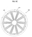
- Figs. 5A-5C illustrate configurations of ten wedge-shaped spiral in-phase current loops 510 that produce a virtual current loop 520. As shown, cancellation of current in adjacent legs of the wedges may take place so that the mid field projection may be produced by the outside legs of the wedges that define the virtual current loop 520 . Since the currents on the outside legs are the same distance from the driving point of the array, they are in-phase. Accordingly, the configurations of Figs. 5A-5C can use a reduced amount of canceling wire, thereby using less power, while generating less far field.
- Fig. 5A illustrates ten identical wedge-shaped three-loop spiral in-phase current loops. It will be understood that any number of wedges may be provided and any number of loops may be provided in the spirals.
- the virtual current loop 520 is created by the in-phase current contributions of the three outer portions 501-503 of the wedges.
- Fig. 5B illustrates a similar configuration to Fig. 5A, except that alternating wedges are mirror images of one another. In this configuration, an even number of wedges preferably are provided.
- the virtual current loop 520 is created by the in-phase current contributions of the three outer portions 501-503 of the wedges.
- the fields created by the legs of adjacent wedges, such as legs 504 and 505 substantially cancel. Improved cancellation may be obtained compared to Fig. 5A because pairs of canceling legs may be the same length and the same distance from the "+" driving point.
- the + and - signs indicate how the array may be driven, with all + points electrically connected together and all - points electrically connected together.
- Fig. 5C illustrates a similar configuration to Fig. 5A, except the legs of the wedges are moved physically closer. They may even be stacked on different layers of a frame or multilayer printed circuit board so that they overlap one another. The closely spaced or overlapping legs can provide improved cancellation so that virtually all the field contribution comes from the virtual current produced by the three outer portions of each wedge. For the same driving current, this configuration can provide less far field and about the same mid field and the same close-in near field as the configuration of Fig. 5A. Thus, the current can be increased dramatically to produce far more mid field, without violating far field regulatory constraints.
- the outer portions of the wedges also may be moved closer together or stacked, as well as the legs of the wedges. This can produce a far field that is the same as if three times the current was flowing in one outer portion.
- the close-in near field also may be approximately three times that of the close-in near field compared to having three legs with 1/3 of the current in each. Accordingly, in contrast with the legs, the outer portions preferably are not moved close together or stacked.
- the mid field projection may be reduced since the mid field distance projection is related to the effective size of the outer portions.
- the outer portion 502 may not project as far as the outer portion 501 .
- the loops preferably are not made too large because the length of the legs may become a larger proportion of the overall length, the inductance may increase and the loop length may become appreciable with respect to the wavelength. The loops also may become too large physically for efficient manufacture and/or use.
- Similar phenomenon may occur if too many loops are used in each spiral wedge.
- the overall loop length may make it difficult to reliably resonate the inductance.
- the inductance may become so large that an unreasonably small capacitance may be needed to resonate at 13.56 MHz.
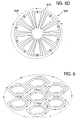
- each wedge may include two or more concentric loops that are wired in parallel, as shown in Fig. 5D.
- Each loop may be driven independently, with its own resonant capacitor or driver circuit. It also will be understood that the configurations of Figs. 5A-5D may be combined, for example to provide a combined spiral and parallel loop approach.
- Fig. 6 illustrates an array of identical hexagonal-shaped in-phase current loops.
- the six-edge pairs of wires can have identical current flowing in opposite directions. Magnetic fields of each of the spirals still project outward and add.
- the virtual current loop 520 projects mid field while allowing reduced far field.
- the current loops can be other polygonal shapes such as squares, triangles, rectangles, etc. and also can be circular or elliptical.
- the array need not be symmetrical, and all the individual loops need not be identical.
- the hexagonal-shaped, in-phase current loops of Fig. 6 may allow shorter wire lengths of the individual loops. The inner segments may cancel well due to equal and opposite currents flowing adjacent to one another.
- peripheral segments do not cancel, and produce the virtual current loop as shown in Fig. 6.
- the virtual current loop may be made larger. Similar effects may be obtained with triangle-shaped current loops.
- Other polygonal shapes such as hexagons may not be nested as well to provide almost complete cancellation of inner segments, due to the configuration of other polygons.
- the arrays of in-phase current loops as illustrated in Figs. 1A, 3A-3C, 5 and 6 may still produce some far field radiation.
- this far field radiation may be further reduced by providing multiple arrays of in-phase current loops wherein each array of in-phase current loops defines a virtual current such that virtual currents of at least some adjacent arrays of in-phase current loops are of differing phase with respect to one another. Since the far field is measured at 30 meters, per FCC Regulations Part 15, multiple arrays of in-phase current loops can produce the opposite radiation at 30 meters and thus cancel at least some more of the far field. By separating identical arrays by small distances, relative to the 22 meter wavelength, the strength of the close-in near and mid fields may not be affected as much as the far field.
- FIG. 7A two arrays 500 and 500' of in-phase current loops are provided that define virtual currents 520 and 520' that are 180° out-of-phase with one another. Stated differently, they are of opposite phase. Although there may be some cancellation of the near field and mid field, there may be a larger amount of cancellation of the far field.
- Fig. 7B illustrates two rows and two columns of arrays of in-phase current loops with alternating clockwise and counter-clockwise virtual current flow. This arrangement may be able to cancel the far field in more directions better than the arrangement of Fig. 7A. It will be understood that the terms “row” and “column” are used herein to indicate two directions that are not necessarily horizontal and vertical.
- Fig. 7C illustrates yet another arrangement wherein a plurality of arrays of in-phase current loops are arranged in a circle with the virtual currents of adjacent arrays being 180 ° out-of-phase with one another.
- the virtual currents of adjacent arrays are 180°/n or 360°/n out-of-phase with one another, where n is the number of arrays of in-phase current loops.
- the virtual currents of a subset of the arrays are 180°/n or 360°/n out-of phase where n is the number of arrays in a subset. Any integer number of subsets may be combined.
- the individual arrays can be rotated to any angle with respect to one another, arranged in any order and/or placed in any pattern close together.
- one or more of the arrays may only include a single current loop.
- an array of single current loops in any of the configurations and/or phase relationships described above may be used to project the mid field while reducing far field radiation.
- Using simple loops may allow less drive circuitry and may be acceptable in portable applications where projection into a relatively large volume may not be needed.
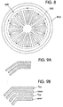
- the array also can use a shield around the outside edge to absorb spurious far field generated by the array. See Fig. 8 which shows a grounded metal shield 810 that can comprise steel or iron, surrounding the outside of an array to reduce spurious far field propagation. It will be understood that the shield may be placed around individual loops, individual arrays or a plurality of arrays.
- the impedance of each spiral may be dependent on the configuration and current flowing in adjacent elements. By controlling the current to thereby match the different impedances of each current loop individually, the overall performance also can be improved.
- the current loops of the present invention may be freestanding wires.
- a supporting frame that supports the wires at various points also may be provided.
- the current loops may be formed on a substrate that can support the entire plurality of arrays of current loops.
- the substrate may be one or more printed circuit boards.
- Multi-layer circuit boards may be utilized to run wires with currents behind or interdigitated with existing elements. See Fig. 9A which illustrates traces on a printed circuit board that may be stacked on different levels and Fig. 9B which illustrates interdigitated top level and interlevel traces.
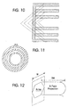
- the edge of the outside spirals may be stacked to promote single line cancellation. Large currents or extreme phase control of the individual turns also may be implemented with concentric loops instead of spirals which may be implemented by multi-layer printed circuit boards. See Fig. 11.
- the receiving device should be electrically matched to the transmitting array.
- the more of the mid field flux lines that go through the receiving loops the more power that generally can be projected. Since the array projects a magnetic field that is initially normal to the plane of the array, tags oriented parallel to the array generally may receive a higher density of flux through them. In some cases, a tag's orientation may be such that so little flux is received that it remains undetected. However, orientation independence can be achieved with different methods.
- a two- or three-dimensional series of loops at the receiving device can increase the likelihood that a certain amount of flux passes through one or more of the loops regardless of orientation.
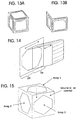
- Fig. 13A which illustrates three loops of wire at a tag, one in each orthogonal dimension to reduce orientation problems.
- Fig. 13B illustrates a two-dimensional version of a receiving device that can capture flux lines that are perpendicular to the planes defining the spirals.
- multiple projecting arrays may be provided. Moreover, rows and columns need not extend in the horizontal and vertical directions. Rather, oblique rows and columns may be provided as illustrated in Fig. 1B. Thus, an increased likelihood that a horizontally or vertically traveling RFID tag will receive enough flux to power the RFID tag may be provided.
- changing the phase and/or magnitude of current through a portion of the projecting array can modify the shape and direction of the projected magnetic field.
- a collimated beam of flux can be moved electronically. See Fig. 14.
- a beam can be moved by changing which part of the array is on or off or by slowly changing the relevant phase and/or magnitude of currents in each element.
- the phase of the plurality of arrays may be changed over time to thereby produce a similar far field while moving nulls of the mid field in space over time.
- the illustrated phase relationships may be maintained for a first time period, such as one second, and second phase relationships may be maintained for succeeding time periods.
- a 60° phase leg may be introduced into each of the plurality of arrays.
- an additional 60° phase leg may be introduced, etc.
- Yet another approach may add one or more arrays that project into the volume. Since magnetic fields add as vectors, the field at any point in the volume is a vector sum of all the contributions of the individual current segments. Thus, changing the magnetic field from any or all of the individual arrays may be used to dynamically change the direction and strength of the field at any point. Finally, multiple arrays may be included, each covering a different dimension of the volume. See Fig. 15 in which three arrays are provided wherein Array 1 can project downward, Array 2 can project to the right and Array 3 can project back in the volume to be covered. Each dimension can then be activated independently. In order to extend the magnetic field even further, additional antennas may be placed directly across from the first with the same field polarity orientation. See Fig. 16. This can almost double the effective distance that can be obtained with a single antenna. Since the magnetic fields add, two arrays oriented in the same direction can effectively double the coverage space. It will be understood that the arrays can be activated independently or together.
- Fig. 17 illustrates a pair of far field cancellation antennas about an array.
- the far field cancellation antennas may be made adaptive. Further reduction of undesired far field generation may be obtained by shielding the connections going to the array, for example, using coaxial cable or shielded twisted wire pair. The effects of current carrying wires from the matching networks to the antenna elements can be reduced by keeping them short, shielded and uniform.
- one or more sensing antennas may be provided to sense communications from the devices.
- the sensing antennas preferably are dipoles. Spatially separated, orthogonally oriented dipoles may be provided to increase the ability to detect communications while reducing the likelihood of destructive interference among the device communications to the antennas.
- the present invention can create mid field magnetic energy that can be made wide and deep without excessive far field generation and without excessive field strength near the antenna structure.
- the magnetic field can be used to operate electronic devices remotely. These electronic devices may include RFID tags, remote sensors such as implanted temperature sensors, and/or remote actuators such as a relay inside a vacuum. Furthermore, other applications desiring a strong-shaped magnetic field for unlicensed operation may benefit from the present invention.
- Fig. 18 illustrates a single ten-inch diameter loop.
- the dot in Fig. 18 and in the remaining figures indicates the X-Y axis location for taking Z axis measurements at 3 meters and at 30 meters.
- the magnetic field at three meters was 0.00421 A/m with a current of 0.81761 amps.
- Fig. 19 is a log/log plot of the H field as a function of distance along the Z axis from one to 100 inches. Accordingly, the close-in near field is indicated to the left of the ten-inch mark in Fig. 19 and the mid field is indicated to the right of the ten-inch mark in Fig. 19.
- the H field at three meters was simulated to be 0.00417 A/m at a current of 0.205317 A.
- a log/log plot of the H field versus distance on the Z axis for a 20-inch loop is shown in Fig. 20.
- Fig. 21 is a log/log plot for the 40-inch diameter loop.
- Fig. 22 illustrates a 20-inch diameter bi-loop which may also be thought of as a pair of in-phase current loop wedges.
- a simulated mid field of 0.00932 A/m was produced at a current of 0.6077701 A.
- Fig. 23 is a log/log plot of the simulated near field and mid field. As shown by comparing Figs. 20 and 23, the 20-inch diameter bi-loop can produce a larger mid field than a 20-inch diameter loop, without violating FCC regulations.
- Fig. 24 illustrates a 20-inch diameter tri-loop.
- a mid field of 0.00933 A/m was simulated at a current of 0.610333 A.
- Fig. 25 graphically illustrates the close-in near field and mid field components.
- Fig. 26 illustrates a 20-inch square loop.
- a mid field of 0.00389 A/m was produced with a current of 0.126952 A. Accordingly, there may not be a large difference between square and circular loops, but the square loop may be easier to fabricate and support.
- Fig. 27 graphically illustrates the close-in near field and mid field for a 20-inch square loop.
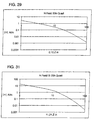
- Fig. 28 illustrates a 20-inch quad wedge. Simulations show that a mid field of 0.000926 A/m may be produced at a current of 0.474899 A. Accordingly, a 20-inch quad wedge can provide a large improvement over a 20-inch diameter loop of Fig. 22.
- Fig. 29 graphically illustrates near field and mid field for the 20-inch quad wedge.
- Fig. 30 illustrates two arrays of 20-inch quad wedges. Simulations indicate that a mid field of 0.001394 A/m is produced at a current of 3.02641 A.
- Fig. 31 graphically illustrates the close-in near field and mid field components.
- Fig. 32 illustrates four 20-inch quad wedge arrays. A very high mid field of 0.02661 A/m was simulated albeit at high current of 38.1075 A.
- Fig. 33 graphically illustrates the close-in near field and mid field of this configuration.
- Fig. 34 illustrates six 20-inch quad wedge arrays. Simulations indicate a magnetic fiela of 0.00119 A/m at a current of 3.02888 A.
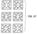
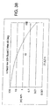
- Fig. 35 illustrates six 20-inch quad wedge arrays wherein adjacent arrays are driven at 60° phase offsets from one another.
- Fig. 35 illustrates phase offsets that are different from 180°. These phase offsets can provide a more spatially uniform near field relative to arrays that have 180° phase differences. Simulations indicate that the array of Fig. 35 can provide a mid field of 0.005598 A/m at a current of 17.6789 A. Accordingly, a very high mid field at more modest current can be provided.
- Fig. 36 graphically illustrates the close-in near field and mid field.
- Fig. 37 illustrates six 20-inch quad wedge spirals at 60° offsets: Fig. 37 differs from Fig. 35 in that each current loop is a two loop spiral current loop. Simulation shows the same mid field as the embodiment of Fig. 35, i.e., 0.0559 A/m, at a reduced current of 9.87382 A. Fig. 38 graphically illustrates the close-in near field and mid field for this configuration. Accordingly, the configuration of Fig. 37 may be most preferred, based on simulations.
- an order-of magnitude more mid field may be produced at 3 meters without violating FCC regulations at 30 meters.
- This order-of magnitude increase in mid field can provide wireless powering of microelectronic devices.
Landscapes
- Engineering & Computer Science (AREA)
- Physics & Mathematics (AREA)
- Health & Medical Sciences (AREA)
- Toxicology (AREA)
- Computer Vision & Pattern Recognition (AREA)
- Artificial Intelligence (AREA)
- General Physics & Mathematics (AREA)
- Theoretical Computer Science (AREA)
- Electromagnetism (AREA)
- General Health & Medical Sciences (AREA)
- Computer Networks & Wireless Communication (AREA)
- Near-Field Transmission Systems (AREA)
- Variable-Direction Aerials And Aerial Arrays (AREA)
- Mobile Radio Communication Systems (AREA)
- Grinding And Polishing Of Tertiary Curved Surfaces And Surfaces With Complex Shapes (AREA)
- Radar Systems Or Details Thereof (AREA)
Claims (25)
- Système de projection par radio fréquence de puissance pour des dispositifs microélectriques de puissance par radiofréquence, le système comprenant :un ensemble (100) d'au moins trois boucles de courant en phase (110a-110d) qui sont disposées adjacentes les unes par rapport aux autres pour définir une surface et pour définir une boucle de courant virtuelle (120) à une périphérie de la surface qui produit un courant virtuel de même direction tandis que le courant dans les parties adjacentes (118a-118d) des boucles de courant adjacentes (110a-110d) circulent dans des directions opposées, projetant ainsi de la puissance par radiofréquence à partir de la surface.
- Un système selon la revendication 1, caractérisé en ce que l'ensemble d'au moins trois boucles de courant en phase comprend un ensemble d'au moins trois boucles de courant cunéiformes, chacune ayant une partie extérieure et une paire de côtés, les au moins trois boucles de courant cunéiformes étant disposées adjacentes les unes par rapport aux autres pour définir une surface de telle manière à ce que les courants dans les parties extérieures sont en phase et le courant dans les côtés adjacents des boucles de courant adjacentes sont en discordance de phase.
- Système selon la revendication 1, caractérisé en ce que l'ensemble d'au moins trois boucles de courant en phase comprend un ensemble d'au moins trois boucles de courant polygonales, chacune ayant une pluralité de côtés, les au moins trois boucles de courant polygonales étant disposées adjacentes les unes par rapport aux autres pour définir une surface, de telle manière à ce que les courants dans les cotés des au moins trois boucles de courant polygonales qui sont adjacentes à la périphérie de la surface sont en phase et le courant dans les cotés adjacents des boucles de courant adjacentes sont en discordance de phase.
- Système selon la revendication 1, caractérisé en ce que l'ensemble d'au moins trois boucles de courant en phase comprend un ensemble d'au moins trois boucles de courant en spiral.
- Système selon la revendication 1, caractérisé en ce que l'ensemble d'au moins trois boucles de courant en phase comprend un ensemble d'au moins trois boucles de courant concentriques.
- Système selon la revendication 1, caractérisé en ce que l'ensemble d'au moins trois boucles de courant en phase comprend un ensemble d'au moins trois boucles de courant superposées.
- Système selon l'une des revendications précédentes comprenant de plus un driver qui pilote l'ensemble des au moins trois boucles de courant à 13,56 MHz pour ainsi projeter par radiofréquence de la puissance.
- Système selon l'une des revendications précédentes, caractérisé en ce que l'ensemble des au moins trois boucles de courant en phase est disposé pour fournir au moins du renforcement d'un champ proche électromagnétique qui est produit par les boucles de courant tout en produisant au moins une compensation d'une onde électromagnétique de champ lointain qui est produite par les boucles de courant.
- Système pour projeter par radiofréquence de la puissance à des dispositifs microélectronique de puissance par radiofréquence, le système comprenant :une pluralité d'ensemble (150) de boucles de courant en phase (100a-100d), les ensembles des boucles de courant en phase étant disposés adjacents les uns par rapport aux autres pour définir une surface, chaque ensemble de boucles de courant en phase définissant un courant virtuel (120a-120d) circulant autour d'une périphérie de l'ensemble des boucles de courant en phase (100a-100d) dans une direction telle que des courants virtuels d'au moins quelques ensembles adjacents de boucles de courant en phase (100a-100d) ne sont pas en phase les uns par rapport aux autres, chaque ensemble de boucles de courant en phase comprenant une pluralité de boucles de courant en phase (110-110d) qui sont disposées adjacentes les unes par rapport aux autres dans la surface, de manière à ce que le courant dans les parties adjacentes (118a-118d) des boucles de courant adjacentes (110a-110d) dans un ensemble circule dans des directions opposées.
- Système selon la revendication 9, caractérisé en ce que les courant virtuels des ensembles adjacents des boucles de courant en phase sont de phase opposée les uns par rapport aux autres.
- Système selon la revendication 9 caractérisé en ce que la pluralité d'ensembles des boucles de courant en phase comprend quatre ensembles de boucles de courant qui sont arrangés en deux rangées et deux colonnes, de telle manière à ce que les courant virtuels dans les ensembles dans chaque rang et chaque colonne sont en opposition de phase.
- Système selon la revendication 9, caractérisé en ce que la pluralité d'ensembles des boucles de courant en phase comprend quatre ensemble de boucles de courant qui sont arrangés en deux rangs et deux colonnes, de telle manière à ce que les courants virtuels dans les ensembles dans chaque rang et chaque colonne sont en discordance de phase de quatre vingt dix degrés les uns par rapport aux autres.
- Système selon l'une des revendications 11 ou 12, caractérisé en ce que les deux rangs et les deux colonnes sont deux rangs obliques et deux colonnes obliques.
- Système selon la revendication 9, caractérisé en ce que la pluralité d'ensemble des boucles de courant en phase comprend une pluralité d'ensembles de boucles de courant qui sont arrangés dans un cercle, de telle manière à ce que les courant virtuels dans des ensembles adjacents dans le cercle sont en opposition de phase.
- Système selon l'une des revendications 9 à 14, caractérisé en ce que chaque ensemble de boucles en phase est arrangé pour fournir au moins quelque renforcement à un champ proche électromagnétique qui est produit par les boucles de courant dans un ensemble tout en produisant au moins quelque compensation d'onde électromagnétique de champ lointain qui est produite pas les boucles de courant dans l'ensemble.
- Système selon la revendication 15, caractérisé en ce que la pluralité d'ensembles de boucles de courant en phase est arrangée pour fournir quelque renforcement supplémentaire des champs proches électromagnétiques qui sont produit par les ensembles de boucles de courant en phase et au moins une compensation supplémentaire des ondes électromagnétiques de champ lointain qui sont produites par les ensembles de boucles de courant en phase.
- Système selon la revendication 9, caractérisé en ce que chaque ensemble de boucles de courant en phase comprend un ensemble d'au moins deux boucles de courant cunéiformes, chacune ayant une partie extérieure et une paire de côtés, les au moins deux boucles de courant cunéiformes étant disposées adjacentes les unes par rapport aux autres pour définir une surface qui est telle que des courants dans les parties extérieures sont en phase et que le courant dans les côtés adjacents des boucles de courants adjacentes sont en discordance de phase.
- Système selon la revendication 9, caractérisé en ce que chaque ensemble de boucles de courant de phase comprend un ensemble d'au moins deux boucles de courant polygonales chacune ayant une pluralité de côtés, les au moins deux boucles de courant polygonales étant disposées adjacentes les unes par rapport aux autres pour définir une surface ayant une limite extérieure, de telle manière à ce que les courants dans les côtés des au moins trois boucles de courant polygonales qui sont adjacentes à la frontière extérieure soient en phase et le courant dans les cotés adjacents des boucles de courant adjacentes soit en discordance de phase.
- Système selon la revendication 9, caractérisé en ce que chaque ensemble de boucles de courant en phase comprend un ensemble de boucles de courant en spirale.
- Système selon l'une des revendications précédentes, caractérisé en ce que chacune des boucles de courant en phase est inférieure à une longueur d'un quart de longueur d'onde.
- Système selon la revendication 9, caractérisé en ce que chaque ensemble de boucles de courant en phase comprend un ensemble de boucles de courant concentriques.
- Système selon la revendication 9, caractérisé en ce que chaque ensemble de boucles de courant en phase comprend un ensemble de boucles de courant empilées.
- Système selon la revendication 9, comprenant de plus un driver qui pilote chaque ensemble de boucles de courant à 13,56 MHz pour projeter par radiofréquence de la puissance.
- Une méthode de projection par radiofréquence de puissance à des dispositifs microélectroniques de puissance par radiofréquence, la méthode comprenant l'étape de :application d'un courant à un ensemble (100) d'au moins trois boucles de courant en phase (110a-110d) qui sont disposées adjacentes les unes par rapport aux autres pour définir une surface et pour définir une boucle de courant virtuelle (120) à une périphérie de la surface qui produit un courant virtuel de même direction tandis que les courants dans les parties adjacentes (118a-118d) des boucles de courant adjacentes (110a-110d) circulent dans des directions opposées, pour ainsi projeter par radiofréquence la puissance à partir de la surface.
- Une méthode de projection de puissance par radiofréquence à des dispositifs micro électroniques de puissance par radiofréquence, la méthode comprenant l'étape de :application d'un courant à pluralité d'ensemble (150) de boucles de courant en phase (100a-100d), les ensembles des boucles de courant en phase étant disposés adjacents les uns par rapport aux autres pour définir une surface, chaque ensemble de boucles de courant en phase définissant un courant virtuel (120a-120d) circulant autour d'une périphérie de l'ensemble de boucles de courant en phase (100a-100d) dans une direction, de telle manière à ce que les courants virtuels d'au moins quelques ensembles adjacents des boucles de courant en phase (100a-100d) sont en discordance de phase-les uns par rapport aux autres, chaque ensemble de boucles de courant en phase (100a-100d) comprenant une pluralité de boucles de courant en phase (110a-110d) qui sont disposées adjacentes les unes par rapport aux autres dans la surface, de telle manière à ce que le courant dans les parties adjacentes (118a-188d) des boucles de courant adjacentes (110a-110d) dans un ensemble circule dans des directions opposées.
Applications Claiming Priority (3)
| Application Number | Priority Date | Filing Date | Title |
|---|---|---|---|
| US8578898P | 1998-05-18 | 1998-05-18 | |
| US85788P | 1998-05-18 | ||
| PCT/US1999/010877 WO1999060512A2 (fr) | 1998-05-18 | 1999-05-17 | Systemes et procedes assurant la fourniture de puissance en radiofrequence via des boucles de courant en phase et permettant l'identification d'etiquettes d'identification en radiofrequence interrogees simultanement |
Publications (2)
| Publication Number | Publication Date |
|---|---|
| EP1078329A2 EP1078329A2 (fr) | 2001-02-28 |
| EP1078329B1 true EP1078329B1 (fr) | 2003-07-16 |
Family
ID=22193945
Family Applications (1)
| Application Number | Title | Priority Date | Filing Date |
|---|---|---|---|
| EP99924290A Expired - Lifetime EP1078329B1 (fr) | 1998-05-18 | 1999-05-17 | Systemes et procedes assurant la fourniture de puissance en radiofrequence via des boucles de courant en phase et permettant l'identification d'etiquettes d'identification en radiofrequence interrogees simultanement |
Country Status (7)
| Country | Link |
|---|---|
| US (2) | US6388628B1 (fr) |
| EP (1) | EP1078329B1 (fr) |
| AT (1) | ATE245292T1 (fr) |
| AU (1) | AU4082599A (fr) |
| DE (2) | DE1078329T1 (fr) |
| ES (1) | ES2164624T1 (fr) |
| WO (1) | WO1999060512A2 (fr) |
Cited By (1)
| Publication number | Priority date | Publication date | Assignee | Title |
|---|---|---|---|---|
| US8115635B2 (en) | 2005-02-08 | 2012-02-14 | Abbott Diabetes Care Inc. | RF tag on test strips, test strip vials and boxes |
Families Citing this family (56)
| Publication number | Priority date | Publication date | Assignee | Title |
|---|---|---|---|---|
| US6960984B1 (en) | 1999-12-08 | 2005-11-01 | University Of North Carolina | Methods and systems for reactively compensating magnetic current loops |
| GB0017882D0 (en) * | 2000-07-21 | 2000-09-06 | Sentec Ltd | Anti collision for passive magnetic tags |
| JP4686109B2 (ja) * | 2000-09-07 | 2011-05-18 | サヴィ テクノロジー,インコーポレイテッド | タグを使用してデバイスを追跡する方法及び装置 |
| US6940392B2 (en) | 2001-04-24 | 2005-09-06 | Savi Technology, Inc. | Method and apparatus for varying signals transmitted by a tag |
| USRE47599E1 (en) | 2000-10-20 | 2019-09-10 | Promega Corporation | RF point of sale and delivery method and system using communication with remote computer and having features to read a large number of RF tags |
| US20020183882A1 (en) | 2000-10-20 | 2002-12-05 | Michael Dearing | RF point of sale and delivery method and system using communication with remote computer and having features to read a large number of RF tags |
| EP1840854B1 (fr) | 2000-10-20 | 2011-04-06 | Promega Corporation | Procédé d'identification par radiofréquence et système de distribution de produits |
| US6708065B2 (en) * | 2001-03-02 | 2004-03-16 | Cardiac Pacemakers, Inc. | Antenna for an implantable medical device |
| US6662048B2 (en) * | 2001-03-30 | 2003-12-09 | Cardiac Pacemakers, Inc. | Implantable medical device with temperature measuring and storing capability |
| US6993393B2 (en) | 2001-12-19 | 2006-01-31 | Cardiac Pacemakers, Inc. | Telemetry duty cycle management system for an implantable medical device |
| US7729776B2 (en) * | 2001-12-19 | 2010-06-01 | Cardiac Pacemakers, Inc. | Implantable medical device with two or more telemetry systems |
| US6985773B2 (en) * | 2002-02-07 | 2006-01-10 | Cardiac Pacemakers, Inc. | Methods and apparatuses for implantable medical device telemetry power management |
| US6819226B2 (en) * | 2002-05-28 | 2004-11-16 | Smartsynch, Incorporated | Systems and methods for energy storage in land-based telemetry applications |
| US7069086B2 (en) | 2002-08-08 | 2006-06-27 | Cardiac Pacemakers, Inc. | Method and system for improved spectral efficiency of far field telemetry in a medical device |
| US20070115132A1 (en) * | 2005-06-10 | 2007-05-24 | Visible Assets, Inc. | Tagging and communication system and methods for use therewith |
| US20050058292A1 (en) * | 2003-09-11 | 2005-03-17 | Impinj, Inc., A Delaware Corporation | Secure two-way RFID communications |
| US7119692B2 (en) * | 2003-11-10 | 2006-10-10 | 3M Innovative Properties Company | System for detecting radio-frequency identification tags |
| US7372364B2 (en) * | 2003-11-10 | 2008-05-13 | 3M Innovative Properties Company | Algorithm for RFID security |
| JP4705952B2 (ja) * | 2004-04-07 | 2011-06-22 | カーディアック ペースメイカーズ, インコーポレイテッド | 埋込み型医療装置におけるrfトランシーバ・デューティ・サイクルのシステムと方法 |
| JP4705953B2 (ja) | 2004-04-07 | 2011-06-22 | カーディアック ペースメイカーズ, インコーポレイテッド | 埋込み型医療装置のrfウエイクアップ |
| ATE413696T1 (de) * | 2004-07-16 | 2008-11-15 | Nxp Bv | Antenne für die kommunikation mit mehreren transpondern |
| US9161231B2 (en) | 2004-10-14 | 2015-10-13 | Alcatel Lucent | Method and system for wireless networking using coordinated dynamic spectrum access |
| US7804411B2 (en) * | 2004-11-15 | 2010-09-28 | Sensormatic Electronics, LLC | Combination EAS and RFID label or tag using a hybrid RFID antenna |
| US7812729B2 (en) * | 2004-11-15 | 2010-10-12 | Sensormatic Electronics, LLC | Combination EAS and RFID label or tag with controllable read range using a hybrid RFID antenna |
| KR100712454B1 (ko) * | 2004-12-27 | 2007-04-27 | 학교법인 포항공과대학교 | 다중검색방법 |
| US7610065B2 (en) * | 2005-02-28 | 2009-10-27 | Cardiac Pacemakers, Inc. | Method and apparatus for antenna selection in a diversity antenna system for communicating with implantable medical device |
| US7128274B2 (en) * | 2005-03-24 | 2006-10-31 | International Business Machines Corporation | Secure credit card with near field communications |
| US7664553B2 (en) * | 2005-04-27 | 2010-02-16 | Cardiac Pacemakers, Inc. | System and method for enabling communications with implantable medical devices |
| JP4226572B2 (ja) * | 2005-05-11 | 2009-02-18 | 株式会社日立国際電気 | リーダライタ装置 |
| US7443362B2 (en) * | 2005-07-19 | 2008-10-28 | 3M Innovative Properties Company | Solenoid antenna |
| WO2007058619A1 (fr) * | 2005-11-19 | 2007-05-24 | Agency For Science, Technology And Research | Antenne de systeme d’identification par radio-frequence |
| US7953096B2 (en) * | 2005-11-23 | 2011-05-31 | Ericsson Ab | Method and system for communication using a partial designated transit list |
| US8805526B2 (en) * | 2006-05-03 | 2014-08-12 | Cardiac Pacemakers, Inc. | Configurable medical telemetry radio system |
| US7613522B2 (en) * | 2006-06-09 | 2009-11-03 | Cardiac Pacemakers, Inc. | Multi-antenna for an implantable medical device |
| US20080186145A1 (en) * | 2007-02-05 | 2008-08-07 | Honeywell International Inc. | Method of cooperation between mobile and fixed rfid readers |
| US8933790B2 (en) * | 2007-06-08 | 2015-01-13 | Checkpoint Systems, Inc. | Phase coupler for rotating fields |
| MX2009013306A (es) * | 2007-06-08 | 2010-02-15 | Checkpoint Systems Inc | Sistema y metodo de deteccion de eas dinamica. |
| US7579995B1 (en) * | 2007-07-30 | 2009-08-25 | Lockheed Martin Corporation | Near field nulling antenna systems |
| US9294157B2 (en) * | 2007-08-20 | 2016-03-22 | Gui-Yang Lu | Radio-frequency identification system |
| JP5439376B2 (ja) * | 2007-09-06 | 2014-03-12 | デカ・プロダクツ・リミテッド・パートナーシップ | Rfidシステム及びその使用方法 |
| AU2013263785B2 (en) * | 2007-11-14 | 2016-06-30 | Sensormatic Electronics, LLC | Combination EAS and RFID label or tag using a hybrid RFID antenna |
| US7796041B2 (en) | 2008-01-18 | 2010-09-14 | Laird Technologies, Inc. | Planar distributed radio-frequency identification (RFID) antenna assemblies |
| US8629650B2 (en) | 2008-05-13 | 2014-01-14 | Qualcomm Incorporated | Wireless power transfer using multiple transmit antennas |
| US9104899B2 (en) * | 2008-08-13 | 2015-08-11 | Infineon Technologies Ag | Multiple transceivers operable as a single transceiver |
| US20100201312A1 (en) | 2009-02-10 | 2010-08-12 | Qualcomm Incorporated | Wireless power transfer for portable enclosures |
| US9312924B2 (en) * | 2009-02-10 | 2016-04-12 | Qualcomm Incorporated | Systems and methods relating to multi-dimensional wireless charging |
| US11476566B2 (en) * | 2009-03-09 | 2022-10-18 | Nucurrent, Inc. | Multi-layer-multi-turn structure for high efficiency wireless communication |
| JP2011259366A (ja) * | 2010-06-11 | 2011-12-22 | Sony Corp | 通信装置 |
| EP2747195B1 (fr) * | 2012-12-21 | 2017-02-08 | Stichting IMEC Nederland | Agencement d'antenne pour alimentation sans fil |
| US9651703B2 (en) | 2014-04-28 | 2017-05-16 | The United States Of America, As Represented By The Secretary Of The Army | Constant phase |
| CN103995250B (zh) * | 2014-05-29 | 2016-08-24 | 南京泰系信息技术有限公司 | 射频标签轨迹追踪方法 |
| JP6392715B2 (ja) * | 2015-08-17 | 2018-09-19 | 日本電信電話株式会社 | ループアンテナアレイ群 |
| JP6062013B1 (ja) * | 2015-09-29 | 2017-01-18 | 日本電信電話株式会社 | 磁界発生装置 |
| JP6069548B1 (ja) * | 2016-01-22 | 2017-02-01 | 日本電信電話株式会社 | ループアンテナアレイ群 |
| EP3474199B1 (fr) * | 2017-10-20 | 2021-05-05 | CL Schutzrechtsverwaltungs GmbH | Procédé de fonctionnement d'un appareil de fabrication additive d'objets tridimensionnels |
| KR102434036B1 (ko) * | 2021-06-17 | 2022-08-19 | 삼성전자주식회사 | 보조 전원 장치의 수명을 위한 충전 전압 제어 방법 및 이를 수행하는 스토리지 장치 |
Family Cites Families (24)
| Publication number | Priority date | Publication date | Assignee | Title |
|---|---|---|---|---|
| US2618746A (en) * | 1948-08-13 | 1952-11-18 | Rca Corp | Antenna system |
| US3925784A (en) | 1971-10-27 | 1975-12-09 | Radiation Inc | Antenna arrays of internally phased elements |
| US4012742A (en) * | 1975-12-29 | 1977-03-15 | International Telephone And Telegraph Corporation | Multimode loop antenna |
| US4243980A (en) | 1978-02-17 | 1981-01-06 | Lichtblau G J | Antenna system for electronic security installations |
| US4373163A (en) | 1980-07-14 | 1983-02-08 | I.D. Engineering, Inc. | Loop antenna for security systems |
| US5223849A (en) * | 1986-11-25 | 1993-06-29 | Chomerics, Inc. | Broadband electromagnetic energy absorber |
| ATE110480T1 (de) | 1987-03-31 | 1994-09-15 | Identec Ltd | Zugangskontrolleinrichtung. |
| US4872018A (en) | 1987-08-31 | 1989-10-03 | Monarch Marking Systems, Inc. | Multiple loop antenna |
| ES2252911T3 (es) * | 1991-04-03 | 2006-05-16 | Tagsys Sa | Sistema de clasificacion de articulos. |
| US5365551A (en) | 1992-12-15 | 1994-11-15 | Micron Technology, Inc. | Data communication transceiver using identification protocol |
| US5500650A (en) | 1992-12-15 | 1996-03-19 | Micron Technology, Inc. | Data communication method using identification protocol |
| US5402134A (en) * | 1993-03-01 | 1995-03-28 | R. A. Miller Industries, Inc. | Flat plate antenna module |
| NL9301650A (nl) | 1993-09-24 | 1995-04-18 | Nedap Nv | Onafhankelijk antennestelsel voor detectiesystemen. |
| US5694139A (en) | 1994-06-28 | 1997-12-02 | Sony Corporation | Short-distance communication antenna and methods of manufacturing and using the short-distance communication antenna |
| US5550547A (en) | 1994-09-12 | 1996-08-27 | International Business Machines Corporation | Multiple item radio frequency tag identification protocol |
| AU702622B2 (en) * | 1995-05-30 | 1999-02-25 | Sensormatic Electronics Corporation | EAS system antenna configuration for providing improved interrogation field distribution |
| US5907221A (en) * | 1995-08-16 | 1999-05-25 | Applied Materials, Inc. | Inductively coupled plasma reactor with an inductive coil antenna having independent loops |
| US5793324A (en) | 1996-01-19 | 1998-08-11 | Texas Instruments Incorporated | Transponder signal collision avoidance system |
| JP2863727B2 (ja) * | 1996-03-08 | 1999-03-03 | 日本アンテナ株式会社 | 単線スパイラルアンテナ |
| US5856788A (en) | 1996-03-12 | 1999-01-05 | Single Chips Systems Corp. | Method and apparatus for radiofrequency identification tags |
| AU2546597A (en) | 1996-04-10 | 1997-10-29 | Sentry Technology Corporation | Electronic article surveillance system |
| US5877728A (en) | 1997-05-28 | 1999-03-02 | Checkpoint Systems, Inc. | Multiple loop antenna |
| US6177806B1 (en) * | 1997-09-03 | 2001-01-23 | International Business Machines Corp. | Signal sensor for rf integrated systems |
| US5963173A (en) * | 1997-12-05 | 1999-10-05 | Sensormatic Electronics Corporation | Antenna and transmitter arrangement for EAS system |
-
1999
- 1999-05-14 US US09/312,577 patent/US6388628B1/en not_active Expired - Fee Related
- 1999-05-17 ES ES99924290T patent/ES2164624T1/es active Pending
- 1999-05-17 WO PCT/US1999/010877 patent/WO1999060512A2/fr not_active Ceased
- 1999-05-17 AT AT99924290T patent/ATE245292T1/de not_active IP Right Cessation
- 1999-05-17 DE DE1078329T patent/DE1078329T1/de active Pending
- 1999-05-17 EP EP99924290A patent/EP1078329B1/fr not_active Expired - Lifetime
- 1999-05-17 AU AU40825/99A patent/AU4082599A/en not_active Abandoned
- 1999-05-17 DE DE69909621T patent/DE69909621D1/de not_active Expired - Lifetime
-
2001
- 2001-11-08 US US10/010,885 patent/US20020084940A1/en not_active Abandoned
Cited By (5)
| Publication number | Priority date | Publication date | Assignee | Title |
|---|---|---|---|---|
| US8115635B2 (en) | 2005-02-08 | 2012-02-14 | Abbott Diabetes Care Inc. | RF tag on test strips, test strip vials and boxes |
| US8223021B2 (en) | 2005-02-08 | 2012-07-17 | Abbott Diabetes Care Inc. | RF tag on test strips, test strip vials and boxes |
| US8358210B2 (en) | 2005-02-08 | 2013-01-22 | Abbott Diabetes Care Inc. | RF tag on test strips, test strip vials and boxes |
| US8390455B2 (en) | 2005-02-08 | 2013-03-05 | Abbott Diabetes Care Inc. | RF tag on test strips, test strip vials and boxes |
| US8542122B2 (en) | 2005-02-08 | 2013-09-24 | Abbott Diabetes Care Inc. | Glucose measurement device and methods using RFID |
Also Published As
| Publication number | Publication date |
|---|---|
| WO1999060512A9 (fr) | 2000-04-20 |
| ES2164624T1 (es) | 2002-03-01 |
| AU4082599A (en) | 1999-12-06 |
| DE1078329T1 (de) | 2002-04-04 |
| WO1999060512A3 (fr) | 2000-02-17 |
| ATE245292T1 (de) | 2003-08-15 |
| EP1078329A2 (fr) | 2001-02-28 |
| US6388628B1 (en) | 2002-05-14 |
| DE69909621D1 (de) | 2003-08-21 |
| WO1999060512A2 (fr) | 1999-11-25 |
| US20020084940A1 (en) | 2002-07-04 |
Similar Documents
| Publication | Publication Date | Title |
|---|---|---|
| EP1078329B1 (fr) | Systemes et procedes assurant la fourniture de puissance en radiofrequence via des boucles de courant en phase et permettant l'identification d'etiquettes d'identification en radiofrequence interrogees simultanement | |
| US6570541B2 (en) | Systems and methods for wirelessly projecting power using multiple in-phase current loops | |
| ES2776023T3 (es) | Antena de múltiples bucles de transmisión/recepción de cancelación de señal para un lector de identificación de radiofrecuencia | |
| EP3320367B1 (fr) | Système et procédé d'identification d'objet | |
| CA2996049C (fr) | Systeme et procede d'identification d'objet | |
| JP2003110338A (ja) | 誘導無線アンテナ、これを用いたデータ通信方法および非接触データ通信装置 | |
| US10031208B2 (en) | Object identification system and method | |
| JP2011125016A (ja) | Rfid通信により物体を位置特定するための装置 | |
| CA2996050C (fr) | Systeme et procede d'identification d'objet | |
| US11300598B2 (en) | Alternative near-field gradient probe for the suppression of radio frequency interference | |
| JP2004199226A (ja) | リーダ/ライタアンテナ及び該アンテナを備えるrfidシステム | |
| Dai et al. | {RFID+}: Spatially controllable identification of {UHF}{RFIDs} via controlled magnetic fields | |
| Michel et al. | Multifunctional modular antenna for near‐field ultra‐high frequency radio frequency identification readers | |
| US11862852B2 (en) | Cable antenna, gate antenna, antenna unit, automatic conveyor shelf and unmanned cash register | |
| Sabesan et al. | An error free passive UHF RFID system using a new form of wireless signal distribution | |
| EP3320366B1 (fr) | Système et procédé d'identification d'objet | |
| EP1238362A1 (fr) | Systemes et procedes permettant de fournir de la puissance en radiofrequence a l'aide de boucles de courant en phase | |
| JP2007043245A (ja) | アンテナ、及びリーダライタ | |
| Chen | Enhancing Signal Coverage for UHF RFID Systems Rui Chen Department of Engineering University of Cambridge | |
| Sarker | Design of multiband centimetre wave antennas for an OFDM based RFID system | |
| HK40075095A (en) | Cable antenna, gate antenna, antenna unit, automatic conveyance rack, and unmanned register | |
| Irfan | Design and Optimization of RFID Systems |
Legal Events
| Date | Code | Title | Description |
|---|---|---|---|
| PUAI | Public reference made under article 153(3) epc to a published international application that has entered the european phase |
Free format text: ORIGINAL CODE: 0009012 |
|
| 17P | Request for examination filed |
Effective date: 20001110 |
|
| AK | Designated contracting states |
Kind code of ref document: A2 Designated state(s): AT BE CH CY DE DK ES FI FR GB GR IE IT LI LU MC NL PT SE |
|
| 17Q | First examination report despatched |
Effective date: 20010307 |
|
| EL | Fr: translation of claims filed | ||
| TCNL | Nl: translation of patent claims filed | ||
| TCAT | At: translation of patent claims filed | ||
| REG | Reference to a national code |
Ref country code: GR Ref legal event code: PP Ref document number: 20020300001 Country of ref document: GR |
|
| REG | Reference to a national code |
Ref country code: ES Ref legal event code: BA2A Ref document number: 2164624 Country of ref document: ES Kind code of ref document: T1 |
|
| DET | De: translation of patent claims | ||
| GRAH | Despatch of communication of intention to grant a patent |
Free format text: ORIGINAL CODE: EPIDOS IGRA |
|
| GRAH | Despatch of communication of intention to grant a patent |
Free format text: ORIGINAL CODE: EPIDOS IGRA |
|
| GRAH | Despatch of communication of intention to grant a patent |
Free format text: ORIGINAL CODE: EPIDOS IGRA |
|
| GRAA | (expected) grant |
Free format text: ORIGINAL CODE: 0009210 |
|
| AK | Designated contracting states |
Designated state(s): AT BE CH CY DE DK ES FI FR GB GR IE IT LI LU MC NL PT SE |
|
| PG25 | Lapsed in a contracting state [announced via postgrant information from national office to epo] |
Ref country code: NL Free format text: LAPSE BECAUSE OF FAILURE TO SUBMIT A TRANSLATION OF THE DESCRIPTION OR TO PAY THE FEE WITHIN THE PRESCRIBED TIME-LIMIT Effective date: 20030716 Ref country code: LI Free format text: LAPSE BECAUSE OF FAILURE TO SUBMIT A TRANSLATION OF THE DESCRIPTION OR TO PAY THE FEE WITHIN THE PRESCRIBED TIME-LIMIT Effective date: 20030716 Ref country code: IT Free format text: LAPSE BECAUSE OF FAILURE TO SUBMIT A TRANSLATION OF THE DESCRIPTION OR TO PAY THE FEE WITHIN THE PRESCRIBED TIME-LIMIT;WARNING: LAPSES OF ITALIAN PATENTS WITH EFFECTIVE DATE BEFORE 2007 MAY HAVE OCCURRED AT ANY TIME BEFORE 2007. THE CORRECT EFFECTIVE DATE MAY BE DIFFERENT FROM THE ONE RECORDED. Effective date: 20030716 Ref country code: FR Free format text: LAPSE BECAUSE OF FAILURE TO SUBMIT A TRANSLATION OF THE DESCRIPTION OR TO PAY THE FEE WITHIN THE PRESCRIBED TIME-LIMIT Effective date: 20030716 Ref country code: FI Free format text: LAPSE BECAUSE OF FAILURE TO SUBMIT A TRANSLATION OF THE DESCRIPTION OR TO PAY THE FEE WITHIN THE PRESCRIBED TIME-LIMIT Effective date: 20030716 Ref country code: CY Free format text: LAPSE BECAUSE OF FAILURE TO SUBMIT A TRANSLATION OF THE DESCRIPTION OR TO PAY THE FEE WITHIN THE PRESCRIBED TIME-LIMIT Effective date: 20030716 Ref country code: CH Free format text: LAPSE BECAUSE OF FAILURE TO SUBMIT A TRANSLATION OF THE DESCRIPTION OR TO PAY THE FEE WITHIN THE PRESCRIBED TIME-LIMIT Effective date: 20030716 Ref country code: BE Free format text: LAPSE BECAUSE OF FAILURE TO SUBMIT A TRANSLATION OF THE DESCRIPTION OR TO PAY THE FEE WITHIN THE PRESCRIBED TIME-LIMIT Effective date: 20030716 Ref country code: AT Free format text: LAPSE BECAUSE OF FAILURE TO SUBMIT A TRANSLATION OF THE DESCRIPTION OR TO PAY THE FEE WITHIN THE PRESCRIBED TIME-LIMIT Effective date: 20030716 |
|
| REG | Reference to a national code |
Ref country code: GB Ref legal event code: FG4D |
|
| REG | Reference to a national code |
Ref country code: CH Ref legal event code: EP |
|
| REG | Reference to a national code |
Ref country code: CH Ref legal event code: NV Representative=s name: MASCHINENFABRIK RIETER AG |
|
| REG | Reference to a national code |
Ref country code: IE Ref legal event code: FG4D |
|
| REF | Corresponds to: |
Ref document number: 69909621 Country of ref document: DE Date of ref document: 20030821 Kind code of ref document: P |
|
| PG25 | Lapsed in a contracting state [announced via postgrant information from national office to epo] |
Ref country code: SE Free format text: LAPSE BECAUSE OF FAILURE TO SUBMIT A TRANSLATION OF THE DESCRIPTION OR TO PAY THE FEE WITHIN THE PRESCRIBED TIME-LIMIT Effective date: 20031016 Ref country code: GR Free format text: LAPSE BECAUSE OF FAILURE TO SUBMIT A TRANSLATION OF THE DESCRIPTION OR TO PAY THE FEE WITHIN THE PRESCRIBED TIME-LIMIT Effective date: 20031016 Ref country code: DK Free format text: LAPSE BECAUSE OF FAILURE TO SUBMIT A TRANSLATION OF THE DESCRIPTION OR TO PAY THE FEE WITHIN THE PRESCRIBED TIME-LIMIT Effective date: 20031016 |
|
| PG25 | Lapsed in a contracting state [announced via postgrant information from national office to epo] |
Ref country code: DE Free format text: LAPSE BECAUSE OF FAILURE TO SUBMIT A TRANSLATION OF THE DESCRIPTION OR TO PAY THE FEE WITHIN THE PRESCRIBED TIME-LIMIT Effective date: 20031017 |
|
| PG25 | Lapsed in a contracting state [announced via postgrant information from national office to epo] |
Ref country code: ES Free format text: LAPSE BECAUSE OF FAILURE TO SUBMIT A TRANSLATION OF THE DESCRIPTION OR TO PAY THE FEE WITHIN THE PRESCRIBED TIME-LIMIT Effective date: 20031027 |
|
| NLV1 | Nl: lapsed or annulled due to failure to fulfill the requirements of art. 29p and 29m of the patents act | ||
| PG25 | Lapsed in a contracting state [announced via postgrant information from national office to epo] |
Ref country code: PT Free format text: LAPSE BECAUSE OF FAILURE TO SUBMIT A TRANSLATION OF THE DESCRIPTION OR TO PAY THE FEE WITHIN THE PRESCRIBED TIME-LIMIT Effective date: 20031216 |
|
| REG | Reference to a national code |
Ref country code: CH Ref legal event code: PL |
|
| PG25 | Lapsed in a contracting state [announced via postgrant information from national office to epo] |
Ref country code: IE Free format text: LAPSE BECAUSE OF NON-PAYMENT OF DUE FEES Effective date: 20040517 Ref country code: GB Free format text: LAPSE BECAUSE OF NON-PAYMENT OF DUE FEES Effective date: 20040517 |
|
| PLBE | No opposition filed within time limit |
Free format text: ORIGINAL CODE: 0009261 |
|
| STAA | Information on the status of an ep patent application or granted ep patent |
Free format text: STATUS: NO OPPOSITION FILED WITHIN TIME LIMIT |
|
| PG25 | Lapsed in a contracting state [announced via postgrant information from national office to epo] |
Ref country code: MC Free format text: LAPSE BECAUSE OF NON-PAYMENT OF DUE FEES Effective date: 20040531 |
|
| 26N | No opposition filed |
Effective date: 20040419 |
|
| EN | Fr: translation not filed | ||
| GBPC | Gb: european patent ceased through non-payment of renewal fee |
Effective date: 20040517 |
|
| REG | Reference to a national code |
Ref country code: IE Ref legal event code: MM4A |
|
| REG | Reference to a national code |
Ref country code: HK Ref legal event code: WD Ref document number: 1035597 Country of ref document: HK |