EP1079434A2 - Structure d'un boítier pour des dispositifs à haut prestation - Google Patents
Structure d'un boítier pour des dispositifs à haut prestation Download PDFInfo
- Publication number
- EP1079434A2 EP1079434A2 EP00118113A EP00118113A EP1079434A2 EP 1079434 A2 EP1079434 A2 EP 1079434A2 EP 00118113 A EP00118113 A EP 00118113A EP 00118113 A EP00118113 A EP 00118113A EP 1079434 A2 EP1079434 A2 EP 1079434A2
- Authority
- EP
- European Patent Office
- Prior art keywords
- external terminal
- power device
- electrode
- mosfet
- terminal
- Prior art date
- Legal status (The legal status is an assumption and is not a legal conclusion. Google has not performed a legal analysis and makes no representation as to the accuracy of the status listed.)
- Withdrawn
Links
Images

Classifications
-
- H—ELECTRICITY
- H10—SEMICONDUCTOR DEVICES; ELECTRIC SOLID-STATE DEVICES NOT OTHERWISE PROVIDED FOR
- H10W—GENERIC PACKAGES, INTERCONNECTIONS, CONNECTORS OR OTHER CONSTRUCTIONAL DETAILS OF DEVICES COVERED BY CLASS H10
- H10W70/00—Package substrates; Interposers; Redistribution layers [RDL]
- H10W70/40—Leadframes
- H10W70/481—Leadframes for devices being provided for in groups H10D8/00 - H10D48/00
-
- H—ELECTRICITY
- H10—SEMICONDUCTOR DEVICES; ELECTRIC SOLID-STATE DEVICES NOT OTHERWISE PROVIDED FOR
- H10W—GENERIC PACKAGES, INTERCONNECTIONS, CONNECTORS OR OTHER CONSTRUCTIONAL DETAILS OF DEVICES COVERED BY CLASS H10
- H10W44/00—Electrical arrangements for controlling or matching impedance
- H10W44/20—Electrical arrangements for controlling or matching impedance at high-frequency [HF] or radio frequency [RF]
-
- H—ELECTRICITY
- H10—SEMICONDUCTOR DEVICES; ELECTRIC SOLID-STATE DEVICES NOT OTHERWISE PROVIDED FOR
- H10W—GENERIC PACKAGES, INTERCONNECTIONS, CONNECTORS OR OTHER CONSTRUCTIONAL DETAILS OF DEVICES COVERED BY CLASS H10
- H10W72/00—Interconnections or connectors in packages
-
- H—ELECTRICITY
- H10—SEMICONDUCTOR DEVICES; ELECTRIC SOLID-STATE DEVICES NOT OTHERWISE PROVIDED FOR
- H10W—GENERIC PACKAGES, INTERCONNECTIONS, CONNECTORS OR OTHER CONSTRUCTIONAL DETAILS OF DEVICES COVERED BY CLASS H10
- H10W44/00—Electrical arrangements for controlling or matching impedance
- H10W44/20—Electrical arrangements for controlling or matching impedance at high-frequency [HF] or radio frequency [RF]
- H10W44/203—Electrical connections
- H10W44/206—Wires
-
- H—ELECTRICITY
- H10—SEMICONDUCTOR DEVICES; ELECTRIC SOLID-STATE DEVICES NOT OTHERWISE PROVIDED FOR
- H10W—GENERIC PACKAGES, INTERCONNECTIONS, CONNECTORS OR OTHER CONSTRUCTIONAL DETAILS OF DEVICES COVERED BY CLASS H10
- H10W72/00—Interconnections or connectors in packages
- H10W72/20—Bump connectors, e.g. solder bumps or copper pillars; Dummy bumps; Thermal bumps
- H10W72/29—Bond pads specially adapted therefor
-
- H—ELECTRICITY
- H10—SEMICONDUCTOR DEVICES; ELECTRIC SOLID-STATE DEVICES NOT OTHERWISE PROVIDED FOR
- H10W—GENERIC PACKAGES, INTERCONNECTIONS, CONNECTORS OR OTHER CONSTRUCTIONAL DETAILS OF DEVICES COVERED BY CLASS H10
- H10W72/00—Interconnections or connectors in packages
- H10W72/50—Bond wires
- H10W72/531—Shapes of wire connectors
- H10W72/5363—Shapes of wire connectors the connected ends being wedge-shaped
-
- H—ELECTRICITY
- H10—SEMICONDUCTOR DEVICES; ELECTRIC SOLID-STATE DEVICES NOT OTHERWISE PROVIDED FOR
- H10W—GENERIC PACKAGES, INTERCONNECTIONS, CONNECTORS OR OTHER CONSTRUCTIONAL DETAILS OF DEVICES COVERED BY CLASS H10
- H10W72/00—Interconnections or connectors in packages
- H10W72/50—Bond wires
- H10W72/531—Shapes of wire connectors
- H10W72/5366—Shapes of wire connectors the bond wires having kinks
-
- H—ELECTRICITY
- H10—SEMICONDUCTOR DEVICES; ELECTRIC SOLID-STATE DEVICES NOT OTHERWISE PROVIDED FOR
- H10W—GENERIC PACKAGES, INTERCONNECTIONS, CONNECTORS OR OTHER CONSTRUCTIONAL DETAILS OF DEVICES COVERED BY CLASS H10
- H10W72/00—Interconnections or connectors in packages
- H10W72/50—Bond wires
- H10W72/541—Dispositions of bond wires
- H10W72/547—Dispositions of multiple bond wires
- H10W72/5473—Dispositions of multiple bond wires multiple bond wires connected to a common bond pad
-
- H—ELECTRICITY
- H10—SEMICONDUCTOR DEVICES; ELECTRIC SOLID-STATE DEVICES NOT OTHERWISE PROVIDED FOR
- H10W—GENERIC PACKAGES, INTERCONNECTIONS, CONNECTORS OR OTHER CONSTRUCTIONAL DETAILS OF DEVICES COVERED BY CLASS H10
- H10W72/00—Interconnections or connectors in packages
- H10W72/50—Bond wires
- H10W72/541—Dispositions of bond wires
- H10W72/547—Dispositions of multiple bond wires
- H10W72/5475—Dispositions of multiple bond wires multiple bond wires connected to common bond pads at both ends of the wires
-
- H—ELECTRICITY
- H10—SEMICONDUCTOR DEVICES; ELECTRIC SOLID-STATE DEVICES NOT OTHERWISE PROVIDED FOR
- H10W—GENERIC PACKAGES, INTERCONNECTIONS, CONNECTORS OR OTHER CONSTRUCTIONAL DETAILS OF DEVICES COVERED BY CLASS H10
- H10W72/00—Interconnections or connectors in packages
- H10W72/50—Bond wires
- H10W72/551—Materials of bond wires
- H10W72/552—Materials of bond wires comprising metals or metalloids, e.g. silver
- H10W72/5522—Materials of bond wires comprising metals or metalloids, e.g. silver comprising gold [Au]
-
- H—ELECTRICITY
- H10—SEMICONDUCTOR DEVICES; ELECTRIC SOLID-STATE DEVICES NOT OTHERWISE PROVIDED FOR
- H10W—GENERIC PACKAGES, INTERCONNECTIONS, CONNECTORS OR OTHER CONSTRUCTIONAL DETAILS OF DEVICES COVERED BY CLASS H10
- H10W72/00—Interconnections or connectors in packages
- H10W72/50—Bond wires
- H10W72/551—Materials of bond wires
- H10W72/552—Materials of bond wires comprising metals or metalloids, e.g. silver
- H10W72/5524—Materials of bond wires comprising metals or metalloids, e.g. silver comprising aluminium [Al]
-
- H—ELECTRICITY
- H10—SEMICONDUCTOR DEVICES; ELECTRIC SOLID-STATE DEVICES NOT OTHERWISE PROVIDED FOR
- H10W—GENERIC PACKAGES, INTERCONNECTIONS, CONNECTORS OR OTHER CONSTRUCTIONAL DETAILS OF DEVICES COVERED BY CLASS H10
- H10W72/00—Interconnections or connectors in packages
- H10W72/50—Bond wires
- H10W72/59—Bond pads specially adapted therefor
-
- H—ELECTRICITY
- H10—SEMICONDUCTOR DEVICES; ELECTRIC SOLID-STATE DEVICES NOT OTHERWISE PROVIDED FOR
- H10W—GENERIC PACKAGES, INTERCONNECTIONS, CONNECTORS OR OTHER CONSTRUCTIONAL DETAILS OF DEVICES COVERED BY CLASS H10
- H10W72/00—Interconnections or connectors in packages
- H10W72/90—Bond pads, in general
- H10W72/921—Structures or relative sizes of bond pads
- H10W72/926—Multiple bond pads having different sizes
-
- H—ELECTRICITY
- H10—SEMICONDUCTOR DEVICES; ELECTRIC SOLID-STATE DEVICES NOT OTHERWISE PROVIDED FOR
- H10W—GENERIC PACKAGES, INTERCONNECTIONS, CONNECTORS OR OTHER CONSTRUCTIONAL DETAILS OF DEVICES COVERED BY CLASS H10
- H10W74/00—Encapsulations, e.g. protective coatings
-
- H—ELECTRICITY
- H10—SEMICONDUCTOR DEVICES; ELECTRIC SOLID-STATE DEVICES NOT OTHERWISE PROVIDED FOR
- H10W—GENERIC PACKAGES, INTERCONNECTIONS, CONNECTORS OR OTHER CONSTRUCTIONAL DETAILS OF DEVICES COVERED BY CLASS H10
- H10W90/00—Package configurations
- H10W90/701—Package configurations characterised by the relative positions of pads or connectors relative to package parts
- H10W90/751—Package configurations characterised by the relative positions of pads or connectors relative to package parts of bond wires
- H10W90/756—Package configurations characterised by the relative positions of pads or connectors relative to package parts of bond wires between a chip and a stacked lead frame, conducting package substrate or heat sink
Definitions
- the present invention relates to a packaging structure of a power device, and more specifically to a type that is used in an element having a high input impedance, such as MOSFET or IGBT.
- a small-size or middle-size power device having an On-state current of 100 [A] or less and a power of 300 [W] or less, has a packaging structure in which semiconductor chips are sealed with resin.
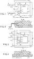
- FIGS. 1 and 2 An example of the packaging structure of a power MOSFET is shown in FIGS. 1 and 2. As shown in these figures, A MOSFET (switching element) is formed on a semiconductor chip 1, and a rear surface of the semiconductor chip 1 becomes to serve as a drain of the MOSFET. The rear surface of the semiconductor chip 1 is fixed to a frame heat radiating section 2-1 by soldering or conductive resin.
- a MOSFET switching element
- the frame heat radiating portion 2-1 has a function of radiating the heat generated within the semiconductor chip 1 to the outside of the package, and further functions as an external terminal (D) of the drain of the MOSFET.
- a source electrode 5 and a gate electrode 6 of the MOSFET are formed on the main surface of the semiconductor chip 1.
- the source electrode 5 is connected to an external terminal (S)2-2 of the source of the MOSFET by a bonding wire 3a.
- the gate electrode 6 is connected to an external terminal (G)2-3 of the source of the MOSFET by a bonding wire 3b.
- the bonding wires 3a and 3b are made of a metal material such as aluminum or gold.
- the semiconductor chip 1 and its peripheral members are covered with the resin 4 and portions of the external terminals (G, D and S) are exposed from the resin 4.
- the locations of the external terminals (G, D and S) may be changed in various ways.
- the position of the external terminal (G) of the gate and that of the external terminal (S) of the source may be switched, or the external terminal (D) of the drain may be provided between the external terminal (G) of the gate and the external terminal (S) of the source so that all the terminals are aligned in one line.
- a power device is used mainly as a switching element which constitutes a DC-DC converter, motor controlling circuit, power source circuit or the like.
- the structure of the power device is mainly of a MOS type having a high impedance. This is because the driving circuit which uses a MOS-type power device has characteristics that the chip size can be reduced, as compared to the driving circuit which uses a bi-polar-type power device.
- the output efficiency of the power device is determined mainly by the on-state power dissipation and turn-on (switching) power dissipation and turn-off (switching) power dissipation. Therefore, conventionally, the objects of the development of power devices are to reduce the On-resistance and to increase the switching speed (that is, to enhance the high-frequency operation property).
- the characteristics of the power MOSFETs and the use conditions have been significantly enhanced over past several years. For example, with regard to the On-resistance, it has been reduced to 1/10 to 1/15 as compared to that of the MOSFETs of several years ago, and the operation frequency has been increased from 50 [kHz] to 100 [kHz].
- the surface mount technology is applied in accordance with the demands of downsizing of the products as well as decreasing the production cost.
- the thinning and downsizing of the electronic parts further are advancing.
- the DIP dual inline package
- the SOP small outline package
- BGA ball grid array
- the package of the power device since it has a simplified SMD structure in which a screw nut portion and an external terminal (pin) of the existing THD (through hole mount device) are simply cut off, and therefore it cannot fully meet the demands of downsizing of the products as well as decreasing the production cost.
- the present invention has been achieved as a solution to the above-described drawbacks, and the object thereof is to provide a power device having a high input impedance, in which even if the operation frequency thereof becomes close to 100 kHz or higher, the improvement of the characteristics of the power device (for example, switching speed) does not peak out, and whose package is suitable for the surface mount.
- the power device of the present invention includes: a semiconductor chip on which a switching element is formed; a package for covering the semiconductor chip; a first lead line connected to a control electrode of the switching element, a second lead line connected to the first electrode of the switching element; third and fourth lead lines both connected to the second electrode of the switching element and separated from each other, wherein an input voltage is applied between the first lead line and the third lead line, and an output current is allowed to flow between the second lead line and the fourth lead line.
- FIG. 3 shows a power device according to the first embodiment of the present invention
- FIG. 4 shows a cross section of the power device shown in FIG. 3.
- This embodiment will be described while taking a surface amount type power MOSFET as an example.
- a vertical-type MOSFET power switching element
- the rear surface of the semiconductor chip 1 serves as a drain of the vertical-type MOSFET.
- the rear surface of the semiconductor chip 1 is fixed to a frame heat radiating portion 2-1 with solder or electroconductive resin.
- the frame heat radiating portion 2-1 has a function of radiating the heat generated in the semiconductor chip 1 to the outside of the package, and further it functions as an external terminal (D) of the drain of the vertical MOSFET.
- a source electrode 5 and a gate electrode 6 of the vertical-type MOSFET are formed on a main surface of the semiconductor chip 1.
- the source electrode 5 is connected to an external terminal (S1) 2-2-1 of a source of the MOSFET via a bonding wire 3a, as well as to an external terminal (S2) 2-2-2 of the source of the MOSFET via a bonding wire 3c.
- the external terminals (S1, S2) 2-2-1 and 2-2-2 are both connected to the source electrode 5 of the vertical MOSFET, but they are separated from each other.
- a gate electrode 6 is connected to an external terminal (G) 2-3 of a gate of the vertical MOSFET via a bonding wire 3b.
- the source external terminal 2-2-1 of the vertical type MOSFET serves as an output terminal for taking out an output current
- the external terminal 2-2-2 serves, together with the external terminal 2-3, as an input terminal for applying an input voltage
- the bonding wires 3a and 3b are made of a metal material such as aluminum (Al) or gold (Au).
- the semiconductor chip 1 and its peripheral portion are covered by a resin 4. However, portions of four external terminals (G, D, S1 and S2) of the vertical MOSFET are exposed from the resin 4.
- the main feature of the above-described power device is that there are two source external terminals of the vertical-type MOSFET.
- the external terminal (S1) 2-2-1 serves as an output terminal for taking out an output current
- the external terminal (S2) 2-2-2 serves, together with the external terminal 2-3, as an input terminal for applying an input voltage.
- the external terminal 2-2-1 is a terminal for taking out an output current, the size thereof is set to be as large as possible. Further, the number of bonding wires 3a for connecting the source electrode 5 and the external terminal 2-2-1 is made as large as possible (for example, in plural).
- the resistance component and inductance component between the source of the vertical-type MOSFET and the external terminal 2-2-1 are made as small as possible by shortening the internal wiring of the semiconductor chip 1, or increasing the number of bonding wires 3a.
- the external terminal 2-2-2 as in the case of the external terminal 2-3, is a terminal for applying an input voltage VGS, and therefore its size may be smaller than that of the external terminal 2-2-1. Further, the number of bonding wires 3c for connecting the source electrode 5 and the external terminal 2-2-2 may be small (for example, one).
- the external terminals 2-2-2 and 2-3 are terminals for applying an input voltage VGS, and therefore in particular, the resistance component and inductance component between the source of the vertical-type MOSFET and the external terminal 2-2-2 would not matter.
- the characteristics of the element for example, switching speed
- This advantage is remarkable particularly in a device having an allowable power dissipation PD of 100 [W] or higher, or in a device which operates at an operation frequency of close to 100 [kHz] or higher. It should be noted here that the specific effect regarding the switching speed will be explained later.
- the above-described power device employs a surface mount type package. Further, since the source external terminal (input terminal) 2-2-2 of the vertical MOSFET and the gate external terminal (input terminal) 2-3 are arranged to be adjacent to each other, the layout of wiring of a board (for example, print circuit board) becomes easy. Consequently, the size of the product (or the system) can be reduced, or the cost can be lowered.
- a board for example, print circuit board
- the position of the gate external terminal 2-3 and that of the source external terminals 2-2-1 and 2-2-2 may be switched over, on a condition that the source external terminal 2-2-1 and the gate external terminal 2-3 are arranged to be adjacent to each other.
- FIG. 5 shows a power device according to the second embodiment of the present invention
- FIG. 6 shoes a cross section of the power device shown in FIG. 5.
- the power device of this embodiment is characterized by an aspect that the device has such a shape which is formed in consideration of the convenience of the mount of the device onto the module device.
- the gate external terminal 2-3 and the two source external terminal 2-2-1 and 2-2-2 are arranged on respective surface sides of the package, and the drain external terminal 2-1 is disposed on the other surface side of the package.
- a vertical-type MOSFET power switching element
- the rear surface of the semiconductor chip 1 serves as a drain of the vertical-type MOSFET.
- the rear surface of the semiconductor chip 1 is fixed to a frame heat radiating portion 2-1 with solder or electroconductive resin.
- the frame heat radiating portion 2-1 has a function of radiating the heat generated in the semiconductor chip 1 to the outside of the package, and further it functions as a drain external terminal (D) of the vertical MOSFET.
- a source electrode 5 and a gate electrode 6 of the vertical-type MOSFET are formed on a main surface of the semiconductor chip 1.
- the source electrode 5 is connected to an external terminal (S1) 2-2-1 of a source of the MOSFET, as well as to an external terminal (S2) 2-2-2 of the source of the MOSFET.
- the external terminals (S1, S2) 2-2-1 and 2-2-2 are both connected to the source electrode 5 of the vertical MOSFET, but they are separated from each other.
- a gate electrode 6 is connected to an external terminal (G) 2-3 of a gate of the vertical MOSFET.
- the source external terminal 2-2-1 of the vertical type MOSFET serves as an output terminal for taking out an output current
- the external terminal 2-2-2 serves, together with the external terminal 2-3, as an input terminal for applying an input voltage
- the semiconductor chip 1 and its peripheral portion are covered by a resin 4. However, portions of four external terminals (G, D, S1 and S2) of the vertical MOSFET are exposed from the resin 4.
- the external terminal (S1) 2-2-1 serves as an output terminal for taking out an output current
- the external terminal (S2) 2-2-2 serves, together with the external terminal 2-3, as an input terminal for applying an input voltage.
- the external terminal (S1) 2-2-1 is a terminal for taking out an output current, the size thereof is set to be as large as possible. Further, the number of contacts (bumps 7a) for connecting the source electrode 5 and the external terminal 2-2-1 is made as large as possible.
- the resistance component and inductance component between the source of the vertical-type MOSFET and the external terminal 2-2-1 are made as small as possible by shortening the internal wiring of the semiconductor chip 1.
- the external terminal (S2) 2-2-2 is a terminal for applying an input voltage VGS, and therefore its size may be smaller than that of the external terminal 2-2-1. Further, the number of contacts (bumps 7c) for connecting the source electrode 5 and the external terminal 2-2-2 may be small.
- the external terminals 2-2-2 and 2-3 are terminals for applying an input voltage VGS, and therefore in particular, the resistance component and inductance component between the source of the vertical-type MOSFET and the external terminal 2-2-2 would not matter.
- the characteristics of the element can be improved.
- This advantage is remarkable particularly in a device having an allowable power dissipation PD of 100 [W] or higher, or in a device which operates at an operation frequency of close to 100 [kHz] or higher.
- bonding wire is not used, and therefore the size of the package can be reduced. Further, the resistance component and inductance component between the source of the vertical-type MOSFET and the external terminal 2-2-1 become lower than those of the power device of the first embodiment described above.
- the source external terminal 2-2-2 and the gate external terminal 2-3 of the vertical-type MOSFET are arranged on the same plane to be adjacent to each other, and therefore the wiring layout on a module device side, that is, mount board (for example, print circuit board) can be facilitated.
- the power device of the present invention has such a package structure that can facilitate the mount of the device onto a module device. As a result, the size of the system can be reduced, and the production cost can be decreased.
- FIG. 7 shows an equivalent circuit to the power device shown in FIGS. 3 to 6.
- VGS denotes a voltage between a gate terminal (external terminal) G and a source terminal (external terminal) S2
- VDS denotes a voltage between a drain terminal (external terminal) D and a source terminal (external terminal) S1
- ID denotes a drain current
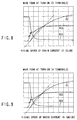
- FIG. 8 indicates results of the measurement of the On-waveform, carried out on a conventional product (three-terminal product), and FIG. 9 indicates results of the measurement of the On-waveform, carried out on a present invention product (four-terminal product).
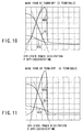
- FIG. 10 indicates results of the measurement of the Off-waveform, carried out on the conventional product (three-terminal product), and FIG. 11 indicates results of the measurement of the Off-waveform, carried out on the present invention product (four-terminal product).
- the turn-on time and turn-off time are both shortened, and therefore a high-speed switching operation can be achieved.
- the results of the comparison between the present invention product and the conventional product are summarized in TABLE 1 below.
- the present invention product achieves the suppression of the switching dissipation by 50% or more as compared to the conventional product.
- the adverse effect which is caused by the drain current ID onto the gate-source voltage (input voltage) VGS can be eliminated. That is, in the conventional case, there is only one source external terminal, which serves, as in the gate external terminal, as a terminal for applying an input voltage VGS as well as a terminal for taking out an output current (drain current). With this structure, there results a great adverse effect of the drain current ID acting on the gate-source voltage VGS.
- the present invention there are two source external terminals, one serving as an input terminal and the other serving as an output terminal.
- the adverse effect of the drain current ID acting on the gate-source voltage VGS can be significantly reduced, and therefore the noise can be decreased.
- the present invention employs a surface mount type package.
- a surface mount type package For example, in the case of such a vertical-type MOSFET as presented above, the contact area between the source terminals S1 and S2 and the print circuit board are remarkably increased, and therefore the generation heat at the external terminals, which occurs when a large current is created, becomes low. Further, since the size of the package is thinned and made small, the size of the overall system can be reduced, and the production cost can be decreased.
- the present invention is directed to a package structure of a power device having a high input impedance, in which the number of source external electrodes of the MOS transistor is set to 2, for example, and therefore with this invention, the characteristics of the element (for example, the switching speed) can be improved.
- This advantage is significant particularly in a device having an allowable power dissipation P D of 100W or higher (for example, a vertical-type MOSFET) or a device having an operation frequency of close to 100 kHz or higher.
- the present invention employs a surface mount type package, the size of the package can be thinned and reduced.
Landscapes
- Wire Bonding (AREA)
- Semiconductor Integrated Circuits (AREA)
Applications Claiming Priority (2)
| Application Number | Priority Date | Filing Date | Title |
|---|---|---|---|
| JP24220699 | 1999-08-27 | ||
| JP24220699A JP2001068498A (ja) | 1999-08-27 | 1999-08-27 | 半導体装置 |
Publications (1)
| Publication Number | Publication Date |
|---|---|
| EP1079434A2 true EP1079434A2 (fr) | 2001-02-28 |
Family
ID=17085840
Family Applications (1)
| Application Number | Title | Priority Date | Filing Date |
|---|---|---|---|
| EP00118113A Withdrawn EP1079434A2 (fr) | 1999-08-27 | 2000-08-25 | Structure d'un boítier pour des dispositifs à haut prestation |
Country Status (4)
| Country | Link |
|---|---|
| EP (1) | EP1079434A2 (fr) |
| JP (1) | JP2001068498A (fr) |
| KR (1) | KR20010070032A (fr) |
| TW (1) | TW499760B (fr) |
Cited By (7)
| Publication number | Priority date | Publication date | Assignee | Title |
|---|---|---|---|---|
| EP2146375A1 (fr) * | 2008-07-16 | 2010-01-20 | Semikron Elektronik GmbH & Co. KG Patentabteilung | Module semi-conducteur |
| US8253225B2 (en) | 2008-02-22 | 2012-08-28 | Infineon Technologies Ag | Device including semiconductor chip and leads coupled to the semiconductor chip and manufacturing thereof |
| US20140103902A1 (en) * | 2012-10-11 | 2014-04-17 | Infineon Technologies Ag | Semiconductor Device Having Sensing Functionality |
| US9165901B2 (en) | 2003-06-30 | 2015-10-20 | Renesas Electronics Corporation | Semiconductor device |
| US10205449B2 (en) | 2016-08-31 | 2019-02-12 | Panasonic Intellectual Property Management Co., Ltd. | Switching circuit |
| DE102013110404B4 (de) | 2012-10-05 | 2019-07-25 | Infineon Technologies Ag | Chipanordnungen und ein Verfahren zum Herstellen einer Chipanordnung |
| CN110149108A (zh) * | 2019-06-05 | 2019-08-20 | 浙江明德微电子股份有限公司 | 一种低功耗的复合sj-mos管及其制备方法 |
Families Citing this family (7)
| Publication number | Priority date | Publication date | Assignee | Title |
|---|---|---|---|---|
| JP4115882B2 (ja) | 2003-05-14 | 2008-07-09 | 株式会社ルネサステクノロジ | 半導体装置 |
| JP5165214B2 (ja) * | 2006-06-26 | 2013-03-21 | オンセミコンダクター・トレーディング・リミテッド | 半導体装置 |
| JP4769784B2 (ja) * | 2007-11-05 | 2011-09-07 | ルネサスエレクトロニクス株式会社 | 半導体装置 |
| JP2013141035A (ja) * | 2013-04-19 | 2013-07-18 | Renesas Electronics Corp | 半導体装置 |
| JP2015019115A (ja) * | 2014-10-28 | 2015-01-29 | ルネサスエレクトロニクス株式会社 | 半導体装置 |
| JP2016040839A (ja) * | 2015-10-27 | 2016-03-24 | ルネサスエレクトロニクス株式会社 | 半導体装置の製造方法 |
| JP6817777B2 (ja) * | 2015-12-16 | 2021-01-20 | ローム株式会社 | 半導体装置 |
-
1999
- 1999-08-27 JP JP24220699A patent/JP2001068498A/ja active Pending
-
2000
- 2000-08-24 KR KR1020000049192A patent/KR20010070032A/ko not_active Abandoned
- 2000-08-25 TW TW089117271A patent/TW499760B/zh active
- 2000-08-25 EP EP00118113A patent/EP1079434A2/fr not_active Withdrawn
Cited By (12)
| Publication number | Priority date | Publication date | Assignee | Title |
|---|---|---|---|---|
| US9165901B2 (en) | 2003-06-30 | 2015-10-20 | Renesas Electronics Corporation | Semiconductor device |
| US9824996B2 (en) | 2003-06-30 | 2017-11-21 | Renesas Electronics Corporation | Semiconductor device having low on resistance |
| US8253225B2 (en) | 2008-02-22 | 2012-08-28 | Infineon Technologies Ag | Device including semiconductor chip and leads coupled to the semiconductor chip and manufacturing thereof |
| US8618644B2 (en) | 2008-02-22 | 2013-12-31 | Infineon Technologies Ag | Electronic device and manufacturing thereof |
| DE102009009874B4 (de) * | 2008-02-22 | 2014-05-15 | Infineon Technologies Ag | Elektronikbauelement mit einem Halbleiterchip und mehreren Zuleitungen |
| EP2146375A1 (fr) * | 2008-07-16 | 2010-01-20 | Semikron Elektronik GmbH & Co. KG Patentabteilung | Module semi-conducteur |
| DE102013110404B4 (de) | 2012-10-05 | 2019-07-25 | Infineon Technologies Ag | Chipanordnungen und ein Verfahren zum Herstellen einer Chipanordnung |
| US20140103902A1 (en) * | 2012-10-11 | 2014-04-17 | Infineon Technologies Ag | Semiconductor Device Having Sensing Functionality |
| US9754854B2 (en) * | 2012-10-11 | 2017-09-05 | Infineon Technologies Ag | Semiconductor device having sensing functionality |
| US10205449B2 (en) | 2016-08-31 | 2019-02-12 | Panasonic Intellectual Property Management Co., Ltd. | Switching circuit |
| US10483966B2 (en) | 2016-08-31 | 2019-11-19 | Panasonic Intellectual Property Management Co., Ltd. | Switching circuit |
| CN110149108A (zh) * | 2019-06-05 | 2019-08-20 | 浙江明德微电子股份有限公司 | 一种低功耗的复合sj-mos管及其制备方法 |
Also Published As
| Publication number | Publication date |
|---|---|
| KR20010070032A (ko) | 2001-07-25 |
| TW499760B (en) | 2002-08-21 |
| JP2001068498A (ja) | 2001-03-16 |
Similar Documents
| Publication | Publication Date | Title |
|---|---|---|
| US7145224B2 (en) | Semiconductor device | |
| US8044468B2 (en) | Semiconductor device | |
| US7227198B2 (en) | Half-bridge package | |
| USRE41719E1 (en) | Power MOSFET with integrated drivers in a common package | |
| KR101086751B1 (ko) | 반도체 장치 및 전원 시스템 | |
| US7776658B2 (en) | Compact co-packaged semiconductor dies with elevation-adaptive interconnection plates | |
| US20030098468A1 (en) | Multi-chip module semiconductor devices | |
| EP1079434A2 (fr) | Structure d'un boítier pour des dispositifs à haut prestation | |
| US20020096748A1 (en) | Back-to -back connected power semiconductor device package | |
| US7019362B2 (en) | Power MOSFET with reduced dgate resistance | |
| JP4250191B2 (ja) | Dc/dcコンバータ用半導体装置 | |
| JP3450803B2 (ja) | 樹脂封止型半導体装置 | |
| US6388319B1 (en) | Three commonly housed diverse semiconductor dice | |
| JP4705945B2 (ja) | 半導体装置 | |
| JP2011181970A (ja) | 半導体装置 | |
| JP4250193B2 (ja) | Dc/dcコンバータ用半導体装置 | |
| US20250096081A1 (en) | Semiconductor package having interposer and method of making the same | |
| JP4800290B2 (ja) | 半導体装置 | |
| TW445607B (en) | Semiconductor device |
Legal Events
| Date | Code | Title | Description |
|---|---|---|---|
| PUAI | Public reference made under article 153(3) epc to a published international application that has entered the european phase |
Free format text: ORIGINAL CODE: 0009012 |
|
| 17P | Request for examination filed |
Effective date: 20000825 |
|
| AK | Designated contracting states |
Kind code of ref document: A2 Designated state(s): AT BE CH CY DE DK ES FI FR GB GR IE IT LI LU MC NL PT SE |
|
| AX | Request for extension of the european patent |
Free format text: AL;LT;LV;MK;RO;SI |
|
| STAA | Information on the status of an ep patent application or granted ep patent |
Free format text: STATUS: THE APPLICATION HAS BEEN WITHDRAWN |
|
| 18W | Application withdrawn |
Withdrawal date: 20020705 |
|
| R18W | Application withdrawn (corrected) |
Effective date: 20020705 |