EP1079437B1 - Détecteur de radiation - Google Patents
Détecteur de radiation Download PDFInfo
- Publication number
- EP1079437B1 EP1079437B1 EP00117472A EP00117472A EP1079437B1 EP 1079437 B1 EP1079437 B1 EP 1079437B1 EP 00117472 A EP00117472 A EP 00117472A EP 00117472 A EP00117472 A EP 00117472A EP 1079437 B1 EP1079437 B1 EP 1079437B1
- Authority
- EP
- European Patent Office
- Prior art keywords
- radiation
- semiconductor layer
- detecting apparatus
- amorphous semiconductor
- radiation detecting
- Prior art date
- Legal status (The legal status is an assumption and is not a legal conclusion. Google has not performed a legal analysis and makes no representation as to the accuracy of the status listed.)
- Expired - Lifetime
Links
- 230000005855 radiation Effects 0.000 title claims description 139
- 239000004065 semiconductor Substances 0.000 claims description 73
- 238000001514 detection method Methods 0.000 claims description 35
- 239000003990 capacitor Substances 0.000 claims description 19
- 239000000969 carrier Substances 0.000 claims description 18
- 239000011669 selenium Substances 0.000 claims description 12
- BUGBHKTXTAQXES-UHFFFAOYSA-N Selenium Chemical compound [Se] BUGBHKTXTAQXES-UHFFFAOYSA-N 0.000 claims description 6
- 239000011159 matrix material Substances 0.000 claims description 6
- 229910052711 selenium Inorganic materials 0.000 claims description 6
- 239000010408 film Substances 0.000 description 41
- 238000002347 injection Methods 0.000 description 16
- 239000007924 injection Substances 0.000 description 16
- 238000012360 testing method Methods 0.000 description 8
- 238000006243 chemical reaction Methods 0.000 description 6
- 238000005259 measurement Methods 0.000 description 6
- 238000000034 method Methods 0.000 description 6
- 239000010409 thin film Substances 0.000 description 6
- 230000035945 sensitivity Effects 0.000 description 5
- 230000000052 comparative effect Effects 0.000 description 4
- 238000010276 construction Methods 0.000 description 4
- 238000002425 crystallisation Methods 0.000 description 4
- 230000008025 crystallization Effects 0.000 description 4
- 229910052959 stibnite Inorganic materials 0.000 description 4
- 239000000758 substrate Substances 0.000 description 4
- 230000002401 inhibitory effect Effects 0.000 description 3
- 229910017255 AsSe Inorganic materials 0.000 description 2
- 229910004613 CdTe Inorganic materials 0.000 description 2
- 229910018321 SbTe Inorganic materials 0.000 description 2
- VYPSYNLAJGMNEJ-UHFFFAOYSA-N Silicium dioxide Chemical compound O=[Si]=O VYPSYNLAJGMNEJ-UHFFFAOYSA-N 0.000 description 2
- 229910007709 ZnTe Inorganic materials 0.000 description 2
- CETPSERCERDGAM-UHFFFAOYSA-N ceric oxide Chemical compound O=[Ce]=O CETPSERCERDGAM-UHFFFAOYSA-N 0.000 description 2
- 229910000422 cerium(IV) oxide Inorganic materials 0.000 description 2
- 238000010586 diagram Methods 0.000 description 2
- 238000009826 distribution Methods 0.000 description 2
- 239000000463 material Substances 0.000 description 2
- 238000012545 processing Methods 0.000 description 2
- 230000036962 time dependent Effects 0.000 description 2
- 238000001771 vacuum deposition Methods 0.000 description 2
- 229910052785 arsenic Inorganic materials 0.000 description 1
- 230000015572 biosynthetic process Effects 0.000 description 1
- 230000015556 catabolic process Effects 0.000 description 1
- 229910052681 coesite Inorganic materials 0.000 description 1
- 150000001875 compounds Chemical class 0.000 description 1
- 238000012790 confirmation Methods 0.000 description 1
- 229910052906 cristobalite Inorganic materials 0.000 description 1
- 239000013078 crystal Substances 0.000 description 1
- 238000002474 experimental method Methods 0.000 description 1
- 239000011521 glass Substances 0.000 description 1
- 229910052737 gold Inorganic materials 0.000 description 1
- 238000003384 imaging method Methods 0.000 description 1
- 229910052738 indium Inorganic materials 0.000 description 1
- 230000000670 limiting effect Effects 0.000 description 1
- 238000004519 manufacturing process Methods 0.000 description 1
- 239000002184 metal Substances 0.000 description 1
- 229910052751 metal Inorganic materials 0.000 description 1
- 229910052759 nickel Inorganic materials 0.000 description 1
- 229910052697 platinum Inorganic materials 0.000 description 1
- 230000002829 reductive effect Effects 0.000 description 1
- 239000000377 silicon dioxide Substances 0.000 description 1
- 229910052682 stishovite Inorganic materials 0.000 description 1
- 229910052905 tridymite Inorganic materials 0.000 description 1
Images



Classifications
-
- G—PHYSICS
- G01—MEASURING; TESTING
- G01T—MEASUREMENT OF NUCLEAR OR X-RADIATION
- G01T1/00—Measuring X-radiation, gamma radiation, corpuscular radiation, or cosmic radiation
- G01T1/16—Measuring radiation intensity
- G01T1/24—Measuring radiation intensity with semiconductor detectors
-
- H—ELECTRICITY
- H10—SEMICONDUCTOR DEVICES; ELECTRIC SOLID-STATE DEVICES NOT OTHERWISE PROVIDED FOR
- H10F—INORGANIC SEMICONDUCTOR DEVICES SENSITIVE TO INFRARED RADIATION, LIGHT, ELECTROMAGNETIC RADIATION OF SHORTER WAVELENGTH OR CORPUSCULAR RADIATION
- H10F39/00—Integrated devices, or assemblies of multiple devices, comprising at least one element covered by group H10F30/00, e.g. radiation detectors comprising photodiode arrays
- H10F39/10—Integrated devices
- H10F39/12—Image sensors
- H10F39/191—Photoconductor image sensors
- H10F39/195—X-ray, gamma-ray or corpuscular radiation imagers
-
- H—ELECTRICITY
- H10—SEMICONDUCTOR DEVICES; ELECTRIC SOLID-STATE DEVICES NOT OTHERWISE PROVIDED FOR
- H10F—INORGANIC SEMICONDUCTOR DEVICES SENSITIVE TO INFRARED RADIATION, LIGHT, ELECTROMAGNETIC RADIATION OF SHORTER WAVELENGTH OR CORPUSCULAR RADIATION
- H10F39/00—Integrated devices, or assemblies of multiple devices, comprising at least one element covered by group H10F30/00, e.g. radiation detectors comprising photodiode arrays
- H10F39/80—Constructional details of image sensors
- H10F39/803—Pixels having integrated switching, control, storage or amplification elements
-
- H—ELECTRICITY
- H10—SEMICONDUCTOR DEVICES; ELECTRIC SOLID-STATE DEVICES NOT OTHERWISE PROVIDED FOR
- H10F—INORGANIC SEMICONDUCTOR DEVICES SENSITIVE TO INFRARED RADIATION, LIGHT, ELECTROMAGNETIC RADIATION OF SHORTER WAVELENGTH OR CORPUSCULAR RADIATION
- H10F77/00—Constructional details of devices covered by this subclass
- H10F77/10—Semiconductor bodies
- H10F77/16—Material structures, e.g. crystalline structures, film structures or crystal plane orientations
- H10F77/162—Non-monocrystalline materials, e.g. semiconductor particles embedded in insulating materials
- H10F77/166—Amorphous semiconductors
-
- Y—GENERAL TAGGING OF NEW TECHNOLOGICAL DEVELOPMENTS; GENERAL TAGGING OF CROSS-SECTIONAL TECHNOLOGIES SPANNING OVER SEVERAL SECTIONS OF THE IPC; TECHNICAL SUBJECTS COVERED BY FORMER USPC CROSS-REFERENCE ART COLLECTIONS [XRACs] AND DIGESTS
- Y02—TECHNOLOGIES OR APPLICATIONS FOR MITIGATION OR ADAPTATION AGAINST CLIMATE CHANGE
- Y02E—REDUCTION OF GREENHOUSE GAS [GHG] EMISSIONS, RELATED TO ENERGY GENERATION, TRANSMISSION OR DISTRIBUTION
- Y02E10/00—Energy generation through renewable energy sources
- Y02E10/50—Photovoltaic [PV] energy
Definitions
- This invention relates to radiation detecting apparatus of the direct conversion type used in the medical, industrial, nuclear and other fields, and more particularly to a technique of suppressing creeping discharges due to a bias voltage applied to a radiation sensitive semiconductor layer.
- Radiation (e.g. X rays) detecting apparatus include the indirect conversion type which first converts radiation (e.g. X rays) into light and then converts the light into electric signals by photoelectric conversion, and the direct conversion type which converts incident radiation directly into electric signals with a radiation sensitive semiconductor layer.
- the latter, direct conversion type apparatus has a voltage application electrode formed on a front surface of the radiation sensitive semiconductor layer to which a predetermined bias voltage is applied, and carrier collection electrodes formed on a back surface of the radiation sensitive semiconductor layer for collecting carriers generated by incident radiation. The carriers are taken out as radiation detection signals, thereby enabling a detection of the radiation.
- Certain of the conventional radiation detecting apparatus of the direct conversion type employ a thick layer of an amorphous semiconductor such as amorphous selenium as the radiation sensitive semiconductor layer.
- An amorphous semiconductor may simply be processed to form a thick and wide layer by vacuum deposition or the like, and therefore is suited for a two-dimensional array structure requiring a large, thick layer.
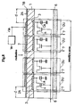
- a two-dimensional array type radiation detecting apparatus known from EP-A-1 009 038 which is a document according to Art. 54 (3) EPC, includes a thick amorphous semiconductor layer 1 for generating electron-hole pairs (carriers) in response to incident radiation, a voltage application electrode 2 formed on the front surface of semiconductor layer 1 to which a bias voltage is applied, and a plurality of carrier collection electrodes 3 arranged in a two-dimensional matrix form on the back surface of semiconductor layer 1.
- Each carrier collection electrode 3 has, connected thereto, a charge storing capacitor Ca and a charge reading switching element (e.g. a thin film transistor) 4 which is normally turned off. Charges accumulating in the capacitors Ca as a result of incident radiation are read as radiation detection signals through the switching elements 4 turned on.
- the radiation detecting apparatus having the two-dimensional array structure shown in Fig. 1 may be used in a fluoroscopic apparatus for detecting transmitted X-ray images.
- fluoroscopic images are acquired based on the radiation detection signals outputted from the radiation detecting apparatus.
- the conventional radiation detecting apparatus noted above has a drawback that the bias voltage applied to the thick amorphous semiconductor layer 1 tends to result in creeping discharges.
- the creeping discharges are caused by dielectric breakdowns occurring along surfaces from edges 2a of the voltage application electrode 2 to edges 1a of the thick amorphous semiconductor layer 1, before being grounded, as shown in Fig. 1.
- the creeping discharges result in noise in the radiation detection signals to become a detriment to image quality.
- the creeping discharges may be suppressed by reducing the bias voltage.
- an amorphous semiconductor is inferior to a single crystal semiconductor in carrier transport characteristics, and cannot demonstrate sufficient detecting sensitivity with a low bias voltage.
- This invention has been made having regard to the state of the art noted above, and its object is to provide a radiation detecting apparatus which suppresses creeping discharges due to a bias voltage applied to a radiation sensitive semiconductor layer.
- radiation to be detected is emitted while a bias voltage is applied to the voltage application electrode formed on the front surface of the radiation sensitive amorphous semiconductor layer. Then, charges accumulate in the charge storing capacitors connected to the carrier collection electrodes, in a quantity corresponding to the carriers generated by incident radiation in the amorphous semiconductor layer. As the charge reading switching elements are turned on, the charges having accumulated are read as radiation detection signals through the switching elements.
- the carrier selectivity of the carrier selective high resistance film blocks an injection of those carriers (electrons or holes) not contributing to the detection of radiation but becoming dark currents, thereby to suppress dark currents. An injection of the carriers that contribute to the detection of radiation is not blocked, thereby to maintain signal response characteristics.
- the surface of the amorphous semiconductor layer is completely covered by the carrier selective high resistance film. This construction prevents crystallization due to moisture and the like of the amorphous semiconductor layer to avoid lowering of the surface resistance.
- the electrodeless region is formed throughout the circumference between edges of the voltage application electrode and edges of the amorphous semiconductor layer.
- the voltage application electrode is surrounded by the carrier selective high resistance film having a high surface resistance. Since sufficient surface voltage endurance is provided between the voltage application electrode and the grounding side, creeping discharges from the radiation sensitive amorphous semiconductor layer due to the bias voltage are suppressed. Consequently, sufficient detection sensitivity is secured by applying a high bias voltage.
- the carrier collection electrodes may be formed in a large number and arranged in a two-dimensional matrix, each of the carrier collection electrodes having one each of the charge storing capacitors and the charge reading switching elements to constitute a two-dimensional array structure. Then, each radiation detecting unit is capable of locally detecting radiation, to enable measurement of a two-dimensional distribution of radiation intensity.
- the carrier selective high resistance film is a p-type conducting film
- a negative bias voltage is applied to the voltage application electrode. This prevents an injection of electrons that do not contribute to the detection of radiation but become dark currents. An injection of holes that contribute to the detection of radiation is allowed, thereby to detect radiation reliably.
- the carrier selective high resistance film is an n-type conducting film
- a positive bias voltage and the n-type carrier selective high resistance film prevent an injection of holes that do not contribute to the detection of radiation but become dark currents, and allows an injection of electrons that contribute to the detection of radiation. Thus, radiation may be detected reliably.
- the electrodeless region preferably, has a width as defined in claim 4.
- the width of the electrodeless region set to the above preferred range, sufficient surface voltage endurance is secured for inhibiting creeping discharges due to the bias current reliably.
- the above range does not substantially diminish the sensitive area (i.e. size of the detecting area) of the amorphous semiconductor layer.
- the creeping discharges due to the bias voltage are suppressed, and at the same time full use is made of the amorphous semiconductor layer suited for realizing an enlarged area.
- the amorphous semiconductor layer preferably, has a thickness in a range of 0.5mm to 1mm. With the thickness of the amorphous semiconductor layer set to the above preferred range, radiation is absorbed sufficiently by the semiconductor layer without passing therethrough.
- the thick amorphous semiconductor layer is formed of amorphous selenium (a-Se).
- a-Se amorphous selenium
- the thick amorphous selenium layer is particularly suited for realizing an enlarged detection area.
- the carrier selective high resistance film preferably, has a surface resistance of at least 10 8 ⁇ / ⁇ . With the surface resistance of the carrier selective high resistance film set to the above preferred value, creeping discharges are suppressed by the high surface resistance.
- the carrier selective high resistance film preferably, has a thickness in a range of 0.01 ⁇ m to 10 ⁇ m. With the thickness of the carrier selective high resistance film set to the above preferred range, an injection of unwanted carriers is inhibited while sufficiently allowing an injection of required carriers.
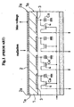
- Fig. 2 is a schematic sectional view showing a radiation sensor of a radiation detecting apparatus in a first embodiment.
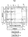
- Fig. 3 is a plan view of the radiation sensor in the first embodiment.
- Fig. 4 is an explanatory view showing a detecting operation of a radiation detecting unit in the first embodiment.
- Fig. 5 is a block diagram showing an entire apparatus in the first embodiment.
- the radiation detecting apparatus in the first embodiment includes a radiation sensor having a thick, radiation sensitive amorphous semiconductor layer 1 for generating carriers in response to incident radiation (e.g. X rays), a voltage application electrode 2 disposed on a front surface, i.e. a radiation incidence side, of semiconductor layer 1, carrier collection electrodes 3 arranged on a back surface, i.e. a radiation non-incidence side (opposite from the radiation incidence side), of semiconductor layer 1, charge storing capacitors Ca for storing carriers collected by the carrier collection electrodes 3, and thin film transistors (TFT) acting as switching elements 4, which are normally turned off (non-conductive), for taking out the charges stored in the capacitors Ca.
- incident radiation e.g. X rays
- a voltage application electrode 2 disposed on a front surface, i.e. a radiation incidence side, of semiconductor layer 1
- carrier collection electrodes 3 arranged on a back surface, i.e. a radiation non-incidence side (opposite from the radiation incidence side
- the apparatus in the first embodiment further includes a bias voltage supply (power source) Ve for applying a negative bias voltage -V A to the voltage application electrode 2.
- the carriers generated by incident radiation, with the bias voltage applied to the voltage application electrode 2 are transferred from the carrier collection electrodes 3 to the capacitors Ca to accumulate therein.
- the switching elements 4 are turned on (connected) whereby the charges are read as radiation detection signals.
- the thick amorphous semiconductor layer 1 is a high purity amorphous selenium (a-Se) layer having a high specific resistance of 10 9 ⁇ cm or more (preferably 10 11 ⁇ cm or more), and a thickness of 0.5mm to 1mm.
- the thick amorphous selenium layer 1 is particularly suited for realizing an enlarged detection area.
- the amorphous semiconductor layer 1, preferably, is as thick as 0.5mm to 1mm, since radiation would just pass through a thin layer without being sufficiently absorbed therein.
- the voltage application electrode 2 and carrier collection electrodes 3 may be formed of a metal selected from Au, Pt, Ni, In and the like, or ITO.
- a metal selected from Au, Pt, Ni, In and the like, or ITO.
- the amorphous semiconductor and electrodes are not limited to the materials cited above.
- the apparatus in the first embodiment includes, as a characterizing feature thereof, a p-type carrier selective high resistance film 1A formed between the amorphous semiconductor layer 1 and voltage application electrode 2 to cover the entire surface of amorphous semiconductor layer 1.
- a p-type carrier selective high resistance film 1A formed between the amorphous semiconductor layer 1 and voltage application electrode 2 to cover the entire surface of amorphous semiconductor layer 1.
- an electrodeless region 2A extends throughout the circumference, with a uniform width d, between the edges of voltage application electrode 2 and the edges of amorphous semiconductor layer 1.
- the p-type carrier selective high resistance film 1A preferably, has a surface resistance (sheet resistance) of 10 8 ⁇ / ⁇ or more, and a film thickness of 0.01 ⁇ m to 10 ⁇ m (usually in the order of 0.1 ⁇ m).
- the film 1A may suitably be formed of Sb 2 S 3 , SbTe, ZnTe, CdTe or AsSe, or may be an organic film.
- a film thickness less than 0.01 ⁇ m would make it difficult to inhibit an injection of unwanted carriers.
- a film thickness exceeding 10 ⁇ m would tend to hamper an injection of required carriers.
- the carrier selective high resistance film 1A covers the amorphous semiconductor layer 1 entirely (100%). However, for expediency of manufacturing or the like, small edge portions of the semiconductor layer 1 may remain uncovered.
- the width d of the electrodeless region preferably, is in the range of Bmm to 3Bmm.
- B is a numerical value when an absolute value of the bias voltage applied by the bias voltage supply Ve is expressed in kV (kilovolt).
- B is 10 and thus the width d of the electrodeless region is in the range of 10mm to 30mm.
- the radiation sensor of the apparatus in the first embodiment includes thin film transistors (of the FET type) acting as the switching elements 4 and the charge storing capacitors Ca, besides the amorphous semiconductor layer 1 and electrodes 2 and 3, all formed on one insulating substrate 6.
- the capacitors Ca are in the form of SiO 2 layers or the like.
- the insulating substrate 6 is in the form of a glass substrate or the like.
- the radiation sensor of the apparatus in the first embodiment has numerous carrier collection electrodes 3 arranged in a two-dimensional matrix.
- Each carrier collection electrode 3 has one charge storing capacitor Ca and one charge reading switching element 4, to constitute one radiation detecting element DU acting as a radiation detecting unit.
- Numerous such radiation detecting elements are arranged along X- and Y-directions (e.g. 1024 ⁇ 1024) to form a flat panel radiation sensor (area sensor) of two-dimensional array structure.
- each radiation detecting unit is capable of locally detecting radiation, to enable measurement of a two-dimensional distribution of radiation intensity.
- the thin film transistors forming the switching elements 4 of detecting elements DU have drains thereof connected to sense lines 7 arranged in the horizontal (X) direction, and gates connected to sense lines 8 arranged in the vertical (Y) direction.
- the sense lines 7 are connected to a multiplexer 10 through a group of charge-to-voltage converters (group of preamplifiers) 9.
- the sense lines 8 are connected to a gate driver 11.
- one charge-to-voltage converter 5 as shown in Fig. 4 is connected to each sense line 7.
- scan signals for fetching signals are inputted to the multiplexer 10 and gate driver 11.
- the detecting elements DU of the radiation sensor are identified by means of addresses (e.g. 0 to 1023) sequentially allocated to the detecting elements DU along the X- and Y-directions.
- the fetching scan signals serve as signals designating the addresses in the X-direction or Y-direction.
- the gate driver 11 applies a fetching voltage to the sense lines 8 arranged in the Y-direction. Then, detecting elements DU are selected on a column-by-column basis.
- the multiplexer 10 is switched by scan signals for the X-direction, the charges stored in the capacitors Ca of the detecting elements DU in the selected columns are successively outputted through the charge-to-voltage converter group 9 and multiplexer 10.
- the radiation detecting apparatus in the first embodiment is used as an X-ray detector of a fluoroscopic apparatus
- detection signals of the detecting elements DU as shown in chain lines in Fig. 5 are successively taken out of the multiplexer 10 as pixel signals.
- an image processor DT performs a necessary signal processing including a noise processing
- an image display MT displays a two-dimensional image (fluoroscopic image).
- the detection signal fetching mode of the radiation sensor in the first embodiment can be said broadly similar to that of ordinary imaging devices such as TV cameras.
- the radiation sensor may include an analog-to-digital converter (not shown), as necessary, in addition to the charge-to-voltage converter group 9, multiplexer 10 and gate driver 11, to promote an integrated construction.
- the charge-to-voltage converter group 9, multiplexer 10, gate driver 11 and the analog-to-digital converter may wholly or partly be installed separately.
- the thin film transistors for switching elements 4, capacitors Ca, carrier collection electrodes 3, amorphous semiconductor layer 1, carrier selective high resistance film 1A and voltage application electrode 2 are successively laminated on a surface of insulating substrate 6 by using the thin film forming technique based on one of various vacuum deposition methods or the pattern forming technique based on a photolithographic method.
- a radiation detecting operation of the radiation detecting apparatus in the first embodiment will be described next with reference to Fig. 4.
- radiation to be detected is emitted while a negative (minus) bias voltage (-V A ) is applied.
- This bias voltage has a polarity for moving holes h, among the carriers generated by incident radiation, toward the voltage application electrode 2 on the front surface of amorphous semiconductor layer 1.
- the carrier selectivity of p-type carrier selective high resistance film 1A blocks the injection of electrons e that do not contribute to the detection of radiation but become dark currents, thereby to suppress dark currents.
- the injection of holes h that contribute to the detection of radiation is not blocked, thereby to maintain signal response characteristics.
- holes h contributing to the detection of radiation are injected through the carrier collection electrode 3 in a large quantity corresponding to the carriers generated by incident radiation, to secure sufficient detection sensitivity.
- charges accumulate in the charge storing capacitors Ca connected to the carrier collection electrodes 3.
- the charge reading switching elements 4 are turned on, the charges having accumulated are read as radiation detection signals through the switching elements 4, and then converted into voltage signals by the charge-to-voltage converters 5.
- the surface of amorphous semiconductor layer 1 is completely covered by the carrier selective high resistance film 1A.
- This construction prevents crystallization due to moisture and the like of the amorphous semiconductor layer 1 to avoid lowering of the surface resistance.
- the electrodeless region 2A is formed throughout the circumference between the edges of voltage application electrode 2 and the edges of amorphous semiconductor layer 1.
- the voltage application electrode 2 is surrounded by the carrier selective high resistance film 1A having a high surface resistance. Since sufficient surface voltage endurance is provided between the voltage application electrode 2 and the grounding side, creeping discharges due to the bias voltage (-V A ) are suppressed.
- the width d of the electrodeless region preferably, is in the range of Bmm to 3Bmm. This range does not substantially diminish the sensitive area (i.e. size of the detecting area) of amorphous semiconductor layer 1 while securing the surface voltage endurance for inhibiting creeping discharges reliably. Thus, the creeping discharges due to the bias voltage are suppressed, and at the same time full use is made of the amorphous semiconductor layer 1 suited for realizing an enlarged area. That is, the width d of the electrodeless region less than Bmm would reduce the length of the carrier selective high resistance film 1A with a high surface resistance and surrounding the voltage application electrode 2, which would make it difficult to secure sufficient insulating voltage endurance. Conversely, where the width d of the electrodeless region limiting the radiation detecting area exceeds 3Bmm, the amorphous semiconductor layer 1 will have a reduced sensitive area (i.e. size of the detecting area).
- a radiation detecting apparatus similar to the radiation detecting apparatus in the first embodiment was constructed for testing purposes.
- the test apparatus was constructed using an a-Se layer having a thickness of 500 ⁇ m as the amorphous semiconductor layer 1, a Sb 2 S 3 film having a thickness in the order of 0.1 ⁇ m as the carrier selective high resistance film 1A, the voltage application electrode 2 being formed on the front surface of amorphous semiconductor layer 1, leaving the electrodeless region with width d of 5mm, and the carrier collection electrodes 3 being formed on the back surface of amorphous semiconductor layer 1.
- a radiation detecting apparatus was constructed for comparison purposes, which was similar to the test radiation detecting apparatus, except that the carrier selective high resistance film 1A was not formed.
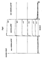
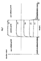
- a negative bias voltage of 1kV was applied to the voltage application electrode 2 of each of the test and comparative radiation detecting apparatus, and detection outputs (current values) of the carrier collection electrodes 3 were measured while an emission of radiation (X rays) was continued from 60 seconds to 120 seconds after a start of bias voltage application.
- Fig. 6 shows measurement results from the test radiation detecting apparatus.
- Fig. 7 shows measurement results from the comparative radiation detecting apparatus.
- Similar measurement was repeated while increasing the bias voltage in steps of 1kV. The measurement was carried out for the test radiation detecting apparatus with bias voltages up to 6kV, and for the comparative radiation detecting apparatus with bias voltages up to 5kV.
- Fig. 8 is a schematic sectional view showing a radiation sensor of a radiation detecting apparatus in a second embodiment.
- Fig. 9 is a plan view of the radiation sensor in the second embodiment.
- Fig. 10 is an explanatory view showing a detecting operation of a radiation detecting unit in the second embodiment.
- the radiation detecting apparatus in the second embodiment includes, between the amorphous semiconductor layer 1 and voltage application electrode 2, an n-type carrier selective high resistance film 1B which is the conducting type opposite to the p-type in the first embodiment. As shown in Fig. 8, a positive bias voltage V A is applied to the voltage application electrode 2.
- the apparatus in this embodiment is the same as the apparatus in the first embodiment. Only the different aspects will be described hereinafter.
- the n-type carrier selective high resistance film 1B preferably, has a surface resistance (sheet resistance) of 10 8 ⁇ / ⁇ or more, and a film thickness of 0.01 ⁇ m to 10 ⁇ m (usually in the order of 0.1 ⁇ m).
- the film 1B may suitably be formed of CdS or CeO 2 .
- a positive (plus) bias voltage (+V A ) is applied.
- This bias voltage has a polarity for moving electrons e, among the carriers generated by incident radiation, toward the voltage application electrode 2 on the front surface of amorphous semiconductor layer 1.
- the carrier selectivity of n-type carrier selective high resistance film 1B blocks the injection of holes h that do not contribute to the detection of radiation but become dark currents, thereby to suppress dark currents.
- the injection of electrons e that contribute to the detection of radiation is not blocked, thereby to maintain signal response characteristics.
- electrons e contributing to the detection of radiation are injected through the carrier collection electrode 3 in a large quantity corresponding to the carriers generated by incident radiation, to secure sufficient detection sensitivity.
- charges accumulate in the charge storing capacitors Ca connected to the carrier collection electrodes 3.
- the charge reading switching elements 4 are turned on, the charges having accumulated are read as radiation detection signals through the switching elements 4, and then converted into voltage signals by the charge-voltage converters 5.
- the surface of amorphous semiconductor layer 1 is completely covered by the carrier selective high resistance film 1B.
- This construction prevents crystallization due to moisture and the like of the amorphous semiconductor layer 1 to avoid lowering of the surface resistance.
- an electrodeless region 2A is formed throughout the circumference between the edges of voltage application electrode 2 and the edges of amorphous semiconductor layer 1.
- the voltage application electrode 2 is surrounded by the carrier selective high resistance film 1B having a high surface resistance. Since sufficient surface voltage endurance is provided between the voltage application electrode 2 and the grounding side, creeping discharges due to the bias voltage (V A ) are suppressed.
Landscapes
- Physics & Mathematics (AREA)
- Health & Medical Sciences (AREA)
- Life Sciences & Earth Sciences (AREA)
- General Physics & Mathematics (AREA)
- High Energy & Nuclear Physics (AREA)
- Molecular Biology (AREA)
- Spectroscopy & Molecular Physics (AREA)
- Measurement Of Radiation (AREA)
- Solid State Image Pick-Up Elements (AREA)
- Light Receiving Elements (AREA)
- Transforming Light Signals Into Electric Signals (AREA)
Claims (9)
- Un détecteur de rayonnement, comprenant une couche à semi-conducteur (1) sensible au rayonnement pour générer des porteurs, c'est-à-dire des paires électron-trou, en réponse à un rayonnement incident, une électrode d'application de tension (2) formée sur une surface avant de la couche à semi-conducteur pour recevoir une tension de polarisation lui étant appliquée, des électrodes de collecte de porteurs (3) portées sur une surface arrière de la couche à semi-conducteur (1), et des condensateurs de stockage de charge (Ca) et des éléments de commutation de lecture de charge (4) connectés aux électrodes de collecte de charge, les charges s'accumulant dans les condensateurs en résultat du rayonnement incident, lu en tant que signaux de détection de rayonnement, par les éléments de commutation mis en service, dans lequel :ladite couche à semi-conducteur (1) sensible au rayonnement est une couche à semi-conducteur amorphe ;un film à haute résistance sélectif aux porteurs (1A) est formé entre ladite couche à semi-conducteur amorphe et ladite électrode d'application de tension (2) pour couvrir entièrement une surface de ladite couche à semi-conducteur amorphe ; et caractérisé parune région sans électrode (2A) sur la surface supérieur du film à haute résistance (1A) qui s'étend sur une circonférence de ladite couche à semi-conducteur amorphe (1), entre le bord extérieur de ladite électrode d'application de tension (2) et le bord extérieur de ladite couche à semi-conducteur amorphe (1).
- Un détecteur de rayonnement tel que défini selon la revendication 1, dans lequel ledit film à haute résistance sélectif aux porteurs (1A) est un film à conduction de type p, et une tension de polarisation négative est appliquée à ladite électrode d'application de tension (2).
- Un détecteur de rayonnement tel que défini selon la revendication 1, dans lequel ledit film à haute résistance sélectif aux porteurs (1A) est un film à conduction de type n, et une tension de polarisation positive est appliquée à ladite électrode d'application de tension (2).
- Un détecteur de rayonnement tel que défini selon la revendication 1, dans lequel ladite région sans électrode (2A) présente une largeur d, définie comme étant d = k x VA, dans laquelle :VA : valeur absolue [kV] de la tension de polarisation ; etk : facteur [mm/kV] ayant une valeur supérieure ou égale à 1 et inférieure ou égale à 3.
- Un détecteur de rayonnement tel que défini à la revendication 1, dans lequel lesdites électrodes de collecte de porteurs (3) sont prévues pour former une matrice bidimensionnelle, chacune desdites électrodes de collecte de porteurs comprenant l'un de chacun desdits condensateurs de stockage de charge (Ca) et desdits éléments de commutation de lecture de charge (4), pour constituer une structure en matrice bidimensionnelle.
- Un détecteur de rayonnement tel que défini à la revendication 1, dans lequel ladite couche à semi-conducteur amorphe (1) présente une épaisseur dans la fourchette de 0,5 mm à 1 mm.
- Un détecteur de rayonnement tel que défini à la revendication 1, dans lequel ladite couche à semi-conducteur amorphe (1) est formée de sélénium amorphe.
- Un détecteur de rayonnement tel que défini à la revendication 1, dans lequel ledit film à haute résistance sélectif aux porteurs (1A) présente une résistance de surface d'au moins 108Ω/□.
- Un détecteur de rayonnement tel que défini à la revendication 1, dans lequel ledit film à haute résistance sélectif aux porteurs (1A) présente une épaisseur dans la fourchette de 0,01 µm à 10µm.
Applications Claiming Priority (2)
| Application Number | Priority Date | Filing Date | Title |
|---|---|---|---|
| JP24002699A JP3832615B2 (ja) | 1999-08-26 | 1999-08-26 | 放射線検出装置 |
| JP24002699 | 1999-08-26 |
Publications (3)
| Publication Number | Publication Date |
|---|---|
| EP1079437A2 EP1079437A2 (fr) | 2001-02-28 |
| EP1079437A3 EP1079437A3 (fr) | 2004-08-18 |
| EP1079437B1 true EP1079437B1 (fr) | 2007-03-14 |
Family
ID=17053373
Family Applications (1)
| Application Number | Title | Priority Date | Filing Date |
|---|---|---|---|
| EP00117472A Expired - Lifetime EP1079437B1 (fr) | 1999-08-26 | 2000-08-11 | Détecteur de radiation |
Country Status (6)
| Country | Link |
|---|---|
| US (1) | US6495817B1 (fr) |
| EP (1) | EP1079437B1 (fr) |
| JP (1) | JP3832615B2 (fr) |
| KR (1) | KR100356115B1 (fr) |
| CN (1) | CN1148807C (fr) |
| DE (1) | DE60033894T2 (fr) |
Families Citing this family (18)
| Publication number | Priority date | Publication date | Assignee | Title |
|---|---|---|---|---|
| JP3678162B2 (ja) * | 2001-04-12 | 2005-08-03 | 株式会社島津製作所 | 放射線検出装置 |
| JP3932857B2 (ja) * | 2001-10-22 | 2007-06-20 | 株式会社島津製作所 | 放射線検出装置 |
| JP3775585B2 (ja) * | 2002-02-08 | 2006-05-17 | 富士写真フイルム株式会社 | 画像記録媒体および製造方法 |
| AU2003247090A1 (en) * | 2002-08-05 | 2004-03-11 | Koninklijke Philips Electronics N.V. | Scanning device including an objective system formed of a single material |
| JP4269859B2 (ja) * | 2003-09-10 | 2009-05-27 | 株式会社島津製作所 | 放射線検出器 |
| JP2005101193A (ja) * | 2003-09-24 | 2005-04-14 | Shimadzu Corp | 放射線検出器 |
| US7928401B2 (en) | 2006-06-14 | 2011-04-19 | Fujifilm Corporation | Radiation detecting system |
| JP5213005B2 (ja) * | 2006-12-18 | 2013-06-19 | 浜松ホトニクス株式会社 | 放射線検出器 |
| JP2008227346A (ja) * | 2007-03-15 | 2008-09-25 | Fujifilm Corp | 放射線検出装置 |
| JP5264291B2 (ja) * | 2007-09-28 | 2013-08-14 | 富士フイルム株式会社 | 放射線検出器 |
| JP2009175102A (ja) * | 2008-01-28 | 2009-08-06 | Shimadzu Corp | 直接変換型x線フラットパネルセンサー |
| CN101577284B (zh) * | 2008-05-09 | 2011-04-13 | 同方威视技术股份有限公司 | 用于测量辐射的半导体探测器及成像装置 |
| CN102414580B (zh) * | 2009-04-30 | 2015-07-22 | 株式会社岛津制作所 | 放射线检测器 |
| KR101042047B1 (ko) * | 2010-05-31 | 2011-06-16 | 주식회사 디알텍 | 리드 아웃 장치 및 이를 이용한 디지털 엑스선 검출장치 |
| KR101042048B1 (ko) * | 2010-05-31 | 2011-06-16 | 주식회사 디알텍 | 리드 아웃 장치 및 이를 이용한 디지털 엑스선 검출장치 |
| US8053856B1 (en) * | 2010-06-11 | 2011-11-08 | Taiwan Semiconductor Manufacturing Company, Ltd. | Backside illuminated sensor processing |
| US10267928B2 (en) * | 2015-11-26 | 2019-04-23 | Koninklijke Philips N.V. | Dark current compensation |
| CN112083470B (zh) * | 2020-09-02 | 2023-11-24 | 重庆中易智芯科技有限责任公司 | 一种阻态敏感CdZnTe辐射探测器及其制造方法 |
Family Cites Families (6)
| Publication number | Priority date | Publication date | Assignee | Title |
|---|---|---|---|---|
| US4233514A (en) * | 1978-12-14 | 1980-11-11 | General Electric Company | Solid state radiation detector and arrays thereof |
| US5101255A (en) * | 1987-01-14 | 1992-03-31 | Sachio Ishioka | Amorphous photoelectric conversion device with avalanche |
| JPH04261071A (ja) * | 1991-01-11 | 1992-09-17 | Canon Inc | 光電変換装置 |
| DE4227096A1 (de) * | 1992-08-17 | 1994-02-24 | Philips Patentverwaltung | Röntgenbilddetektor |
| US5986285A (en) * | 1996-11-07 | 1999-11-16 | Fuji Xerox, Co., Ltd. | Group III-V amorphous and microcrystalline optical semiconductor including hydrogen, and method of forming thereof |
| JP4059463B2 (ja) * | 1998-12-10 | 2008-03-12 | 株式会社島津製作所 | 放射線検出装置 |
-
1999
- 1999-08-26 JP JP24002699A patent/JP3832615B2/ja not_active Expired - Lifetime
-
2000
- 2000-08-11 EP EP00117472A patent/EP1079437B1/fr not_active Expired - Lifetime
- 2000-08-11 DE DE60033894T patent/DE60033894T2/de not_active Expired - Lifetime
- 2000-08-16 US US09/639,086 patent/US6495817B1/en not_active Expired - Lifetime
- 2000-08-22 CN CNB001238477A patent/CN1148807C/zh not_active Expired - Fee Related
- 2000-08-24 KR KR1020000049218A patent/KR100356115B1/ko not_active Expired - Fee Related
Also Published As
| Publication number | Publication date |
|---|---|
| CN1148807C (zh) | 2004-05-05 |
| DE60033894D1 (de) | 2007-04-26 |
| EP1079437A2 (fr) | 2001-02-28 |
| CN1286406A (zh) | 2001-03-07 |
| DE60033894T2 (de) | 2007-12-06 |
| JP3832615B2 (ja) | 2006-10-11 |
| KR20010067103A (ko) | 2001-07-12 |
| EP1079437A3 (fr) | 2004-08-18 |
| US6495817B1 (en) | 2002-12-17 |
| KR100356115B1 (ko) | 2002-10-12 |
| JP2001068656A (ja) | 2001-03-16 |
Similar Documents
| Publication | Publication Date | Title |
|---|---|---|
| US6495817B1 (en) | Radiation detecting apparatus having an electrodeless region | |
| KR100451540B1 (ko) | 방사선 검출장치 | |
| EP0722188B1 (fr) | Panneau de capture d'image utilisant un dispositif à l'état solide | |
| US5930591A (en) | High resolution, low voltage flat-panel radiation imaging sensors | |
| EP1300885B1 (fr) | Détecteur de rayons X à écran plat | |
| USRE42157E1 (en) | Photoelectric converter, its driving method, and system including the photoelectric converter | |
| EP1933381B1 (fr) | Procédé de lecture de signal d'image et système de lecture de signal d'image | |
| EP0780903B1 (fr) | Dispositif de prise de vue de type à panneau plat comprenant une électrode commune à motifs | |
| US8039809B2 (en) | Sensor panel and image detecting device | |
| JP3833712B2 (ja) | 捕捉電荷が減少する放射線イメージング用フラットパネル検出器 | |
| US6528794B1 (en) | Radiation detecting apparatus | |
| EP2023163A2 (fr) | Dispositif de détection d'image | |
| US5780858A (en) | Electromagnetic radiation imaging device using dual gate thin film transistors | |
| US7705282B2 (en) | EDS protection for an image detecting device | |
| EP1073267A2 (fr) | Capteur d'image de rayonnement | |
| JP2005033002A (ja) | 放射線検出器およびその製造方法 | |
| JP2002009268A (ja) | 放射線検出装置 | |
| CA2228116A1 (fr) | Detecteur de panneau de radiographie a charges-pieges reduites |
Legal Events
| Date | Code | Title | Description |
|---|---|---|---|
| PUAI | Public reference made under article 153(3) epc to a published international application that has entered the european phase |
Free format text: ORIGINAL CODE: 0009012 |
|
| AK | Designated contracting states |
Kind code of ref document: A2 Designated state(s): AT BE CH CY DE DK ES FI FR GB GR IE IT LI LU MC NL PT SE |
|
| AX | Request for extension of the european patent |
Free format text: AL;LT;LV;MK;RO;SI |
|
| PUAL | Search report despatched |
Free format text: ORIGINAL CODE: 0009013 |
|
| AK | Designated contracting states |
Kind code of ref document: A3 Designated state(s): AT BE CH CY DE DK ES FI FR GB GR IE IT LI LU MC NL PT SE |
|
| AX | Request for extension of the european patent |
Extension state: AL LT LV MK RO SI |
|
| 17P | Request for examination filed |
Effective date: 20050125 |
|
| AKX | Designation fees paid |
Designated state(s): DE FR NL |
|
| RBV | Designated contracting states (corrected) |
Designated state(s): DE FR NL |
|
| GRAP | Despatch of communication of intention to grant a patent |
Free format text: ORIGINAL CODE: EPIDOSNIGR1 |
|
| RAP1 | Party data changed (applicant data changed or rights of an application transferred) |
Owner name: SHINDENGEN SENSOR DEVICE CO., LTD. Owner name: SHINDENGEN ELECTRIC MANUFACTURING COMPANY, LIMITED Owner name: SHIMADZU CORPORATION |
|
| GRAS | Grant fee paid |
Free format text: ORIGINAL CODE: EPIDOSNIGR3 |
|
| GRAA | (expected) grant |
Free format text: ORIGINAL CODE: 0009210 |
|
| AK | Designated contracting states |
Kind code of ref document: B1 Designated state(s): DE FR NL |
|
| REF | Corresponds to: |
Ref document number: 60033894 Country of ref document: DE Date of ref document: 20070426 Kind code of ref document: P |
|
| ET | Fr: translation filed | ||
| PLBE | No opposition filed within time limit |
Free format text: ORIGINAL CODE: 0009261 |
|
| STAA | Information on the status of an ep patent application or granted ep patent |
Free format text: STATUS: NO OPPOSITION FILED WITHIN TIME LIMIT |
|
| 26N | No opposition filed |
Effective date: 20071217 |
|
| REG | Reference to a national code |
Ref country code: NL Ref legal event code: SD Effective date: 20110117 |
|
| REG | Reference to a national code |
Ref country code: FR Ref legal event code: TP |
|
| REG | Reference to a national code |
Ref country code: DE Ref legal event code: R082 Ref document number: 60033894 Country of ref document: DE Representative=s name: KILIAN KILIAN & PARTNER MBB PATENTANWAELTE, DE Effective date: 20110707 Ref country code: DE Ref legal event code: R082 Ref document number: 60033894 Country of ref document: DE Representative=s name: WILHELMS, KILIAN & PARTNER, DE Effective date: 20110707 Ref country code: DE Ref legal event code: R081 Ref document number: 60033894 Country of ref document: DE Owner name: SHIMADZU CORP., JP Free format text: FORMER OWNER: SHIMADZU CORP., SHINDENGEN ELECTRIC MFG. CO. LT, SHINDENGEN SENSOR DEVICE CO., L, , JP Effective date: 20110707 Ref country code: DE Ref legal event code: R082 Ref document number: 60033894 Country of ref document: DE Representative=s name: KILIAN KILIAN & PARTNER, DE Effective date: 20110707 Ref country code: DE Ref legal event code: R081 Ref document number: 60033894 Country of ref document: DE Owner name: SHIMADZU CORP., JP Free format text: FORMER OWNERS: SHIMADZU CORP., KYOTO-SHI, JP; SHINDENGEN ELECTRIC MFG. CO. LTD., TOKIO/TOKYO, JP; SHINDENGEN SENSOR DEVICE CO., LTD., KOFU, YAMANASHI, JP Effective date: 20110707 |
|
| REG | Reference to a national code |
Ref country code: DE Ref legal event code: R082 Ref document number: 60033894 Country of ref document: DE Representative=s name: KILIAN KILIAN & PARTNER MBB PATENTANWAELTE, DE Ref country code: DE Ref legal event code: R082 Ref document number: 60033894 Country of ref document: DE Representative=s name: KILIAN KILIAN & PARTNER, DE |
|
| REG | Reference to a national code |
Ref country code: FR Ref legal event code: PLFP Year of fee payment: 16 |
|
| PGFP | Annual fee paid to national office [announced via postgrant information from national office to epo] |
Ref country code: NL Payment date: 20150709 Year of fee payment: 16 |
|
| PGFP | Annual fee paid to national office [announced via postgrant information from national office to epo] |
Ref country code: DE Payment date: 20150804 Year of fee payment: 16 |
|
| PGFP | Annual fee paid to national office [announced via postgrant information from national office to epo] |
Ref country code: FR Payment date: 20150629 Year of fee payment: 16 |
|
| REG | Reference to a national code |
Ref country code: DE Ref legal event code: R119 Ref document number: 60033894 Country of ref document: DE |
|
| REG | Reference to a national code |
Ref country code: NL Ref legal event code: MM Effective date: 20160901 |
|
| REG | Reference to a national code |
Ref country code: FR Ref legal event code: ST Effective date: 20170428 |
|
| PG25 | Lapsed in a contracting state [announced via postgrant information from national office to epo] |
Ref country code: NL Free format text: LAPSE BECAUSE OF NON-PAYMENT OF DUE FEES Effective date: 20160901 |
|
| PG25 | Lapsed in a contracting state [announced via postgrant information from national office to epo] |
Ref country code: DE Free format text: LAPSE BECAUSE OF NON-PAYMENT OF DUE FEES Effective date: 20170301 Ref country code: FR Free format text: LAPSE BECAUSE OF NON-PAYMENT OF DUE FEES Effective date: 20160831 |