EP1081544A1 - Dispositif et procédé pour projeter une image digitale sur un matériau photosensible - Google Patents
Dispositif et procédé pour projeter une image digitale sur un matériau photosensible Download PDFInfo
- Publication number
- EP1081544A1 EP1081544A1 EP00113646A EP00113646A EP1081544A1 EP 1081544 A1 EP1081544 A1 EP 1081544A1 EP 00113646 A EP00113646 A EP 00113646A EP 00113646 A EP00113646 A EP 00113646A EP 1081544 A1 EP1081544 A1 EP 1081544A1
- Authority
- EP
- European Patent Office
- Prior art keywords
- light
- light modulators
- partial images
- lighting unit
- beam splitter
- Prior art date
- Legal status (The legal status is an assumption and is not a legal conclusion. Google has not performed a legal analysis and makes no representation as to the accuracy of the status listed.)
- Granted
Links
Images


Classifications
-
- H—ELECTRICITY
- H04—ELECTRIC COMMUNICATION TECHNIQUE
- H04N—PICTORIAL COMMUNICATION, e.g. TELEVISION
- H04N1/00—Scanning, transmission or reproduction of documents or the like, e.g. facsimile transmission; Details thereof
- H04N1/04—Scanning arrangements, i.e. arrangements for the displacement of active reading or reproducing elements relative to the original or reproducing medium, or vice versa
- H04N1/19—Scanning arrangements, i.e. arrangements for the displacement of active reading or reproducing elements relative to the original or reproducing medium, or vice versa using multi-element arrays
- H04N1/191—Scanning arrangements, i.e. arrangements for the displacement of active reading or reproducing elements relative to the original or reproducing medium, or vice versa using multi-element arrays the array comprising a one-dimensional [1D] array
- H04N1/192—Simultaneously or substantially simultaneously scanning picture elements on one main scanning line
- H04N1/193—Simultaneously or substantially simultaneously scanning picture elements on one main scanning line using electrically scanned linear arrays, e.g. linear CCD arrays
-
- G—PHYSICS
- G02—OPTICS
- G02B—OPTICAL ELEMENTS, SYSTEMS OR APPARATUS
- G02B26/00—Optical devices or arrangements for the control of light using movable or deformable optical elements
- G02B26/08—Optical devices or arrangements for the control of light using movable or deformable optical elements for controlling the direction of light
- G02B26/0816—Optical devices or arrangements for the control of light using movable or deformable optical elements for controlling the direction of light by means of one or more reflecting elements
- G02B26/0833—Optical devices or arrangements for the control of light using movable or deformable optical elements for controlling the direction of light by means of one or more reflecting elements the reflecting element being a micromechanical device, e.g. a MEMS mirror, DMD
-
- G—PHYSICS
- G02—OPTICS
- G02B—OPTICAL ELEMENTS, SYSTEMS OR APPARATUS
- G02B27/00—Optical systems or apparatus not provided for by any of the groups G02B1/00 - G02B26/00, G02B30/00
- G02B27/10—Beam splitting or combining systems
- G02B27/1066—Beam splitting or combining systems for enhancing image performance, like resolution, pixel numbers, dual magnifications or dynamic range, by tiling, slicing or overlapping fields of view
-
- G—PHYSICS
- G02—OPTICS
- G02B—OPTICAL ELEMENTS, SYSTEMS OR APPARATUS
- G02B27/00—Optical systems or apparatus not provided for by any of the groups G02B1/00 - G02B26/00, G02B30/00
- G02B27/10—Beam splitting or combining systems
- G02B27/14—Beam splitting or combining systems operating by reflection only
- G02B27/144—Beam splitting or combining systems operating by reflection only using partially transparent surfaces without spectral selectivity
-
- G—PHYSICS
- G02—OPTICS
- G02B—OPTICAL ELEMENTS, SYSTEMS OR APPARATUS
- G02B27/00—Optical systems or apparatus not provided for by any of the groups G02B1/00 - G02B26/00, G02B30/00
- G02B27/10—Beam splitting or combining systems
- G02B27/14—Beam splitting or combining systems operating by reflection only
- G02B27/145—Beam splitting or combining systems operating by reflection only having sequential partially reflecting surfaces
-
- G—PHYSICS
- G03—PHOTOGRAPHY; CINEMATOGRAPHY; ANALOGOUS TECHNIQUES USING WAVES OTHER THAN OPTICAL WAVES; ELECTROGRAPHY; HOLOGRAPHY
- G03B—APPARATUS OR ARRANGEMENTS FOR TAKING PHOTOGRAPHS OR FOR PROJECTING OR VIEWING THEM; APPARATUS OR ARRANGEMENTS EMPLOYING ANALOGOUS TECHNIQUES USING WAVES OTHER THAN OPTICAL WAVES; ACCESSORIES THEREFOR
- G03B27/00—Photographic printing apparatus
- G03B27/32—Projection printing apparatus, e.g. enlarger, copying camera
-
- H—ELECTRICITY
- H04—ELECTRIC COMMUNICATION TECHNIQUE
- H04N—PICTORIAL COMMUNICATION, e.g. TELEVISION
- H04N1/00—Scanning, transmission or reproduction of documents or the like, e.g. facsimile transmission; Details thereof
- H04N1/04—Scanning arrangements, i.e. arrangements for the displacement of active reading or reproducing elements relative to the original or reproducing medium, or vice versa
- H04N1/19—Scanning arrangements, i.e. arrangements for the displacement of active reading or reproducing elements relative to the original or reproducing medium, or vice versa using multi-element arrays
- H04N1/191—Scanning arrangements, i.e. arrangements for the displacement of active reading or reproducing elements relative to the original or reproducing medium, or vice versa using multi-element arrays the array comprising a one-dimensional [1D] array
- H04N1/192—Simultaneously or substantially simultaneously scanning picture elements on one main scanning line
- H04N1/193—Simultaneously or substantially simultaneously scanning picture elements on one main scanning line using electrically scanned linear arrays, e.g. linear CCD arrays
- H04N1/1934—Combination of arrays
Definitions
- the invention relates to a device and a method for exposing a digital image on light-sensitive material according to the preamble of claim 1 and claim 10.
- Such devices and methods are different Applications dealing with digital imaging devices, known.
- DE-PS 42 11 1208 An example is disclosed in DE-PS 42 11 128, in which an image transmission method is described. With this method, an image template is point and scanned line by line, the individual signals are digitized and the digital ones Image signals by means of a light modulator illuminated by a light source an optic exposed on photo paper.
- This procedure is suitable for exposure procedures where it is not based on the rapid production of many pictures is well received. It offers z. B. for manufacturing from less frequent index prints between standard exposures. The loss of time due to the successive exposure of the partial images and also the calibration required between exposures can be purchased be taken. The exposure of an entire digital image takes at This procedure takes too long to process with a photographic copier in which images are to be continuously exposed.
- a special problem of this arrangement arises from the fact that the illumination and imaging beam path are spatially sufficiently far apart must be separated so that the imaging beam path is not separated from the illumination optics is vignetted. This spatial separation prevents a compact Structure of the exposure system.
- the decoupled light is sent to a sensor and there is monitored whether the exposure in the impact area is even he follows. This means that a continuous correction can be made even during the exposure the density in the joint area.
- This arrangement is disadvantageous however, as with the previous one, that a very compact structure is impossible is because the illumination and imaging beam path are spatially separated have to be. Furthermore, it is problematic with such arrangements, the two Adjust light modulators so that their images collide exactly on the photo paper.
- the object of the invention was therefore to provide a device for digital exposure Images in which partial images generated on different light modulators simultaneously are imaged side by side on light-sensitive material, so that that with a compact, adjustment-friendly construction of the Device no jumps in density occur at the joint areas of the partial images.
- prism complexes When using prism complexes, they are constructed and arranged so that the rays emitted by the lighting device under hit the prism interfaces at such a small angle that at Transition to the optically thinner medium at the respective interface on the Light modulator are totally reflected. Those reflected by the light modulator Beams hit the interface of the beam splitter prisms at a different angle than the incident rays so that they pass through the interfaces can. During transmission, the rays are deflected so that they are together with the rays reflected by other light modulators behind the Beam splitter prisms result in a common bundle of rays that on the light-sensitive material exposed a gapless image.
- VFDs Digital Micro Mirror Devices
- VFDs can be used as light modulators (Vacuum fluorescence displays), reflective LCDs, GLVs (Grating Light Valve) or any other reflective light modulator can be used.
- the beam splitter complex and lighting arrangement can compose partial images of any number of light modulators become. Although doing an even number of light modulators For reasons of symmetry, it is fundamentally also odd Numbers of light modulators can be combined.
- Metallic physical beam splitters have that Advantage that they hardly change the color of the split light, so that Composite image does not need to be corrected in color, however they do the disadvantage of a large loss of light.
- All possible multicolored light sources are suitable as the lighting unit, such as B. halogen lamps or LEDs, the light with beam splitters in a common Beam path is combined. It is only important for the lighting that the light for all light modulators comes from the same light source if possible.
- the light from the lighting unit be directed directly to the light modulators or the light of the Lighting unit is first divided by additional beam splitters so that there are several virtual images of this one light source, each then illuminate a light modulator.
- the arrangement of the lighting unit, lighting optics, beam splitter complex, Light modulators and imaging optics should be symmetrical so that both the beam paths that illuminate the light modulators and the Beam paths that the image generated on the light modulators on the photosensitive Show material that is the same length for each light modulator. This is the prerequisite for realizing a Köhler beam path can.
- the lighting optics must be arranged and constructed that the image of the light source is imaged in the pupil of the imaging optics, and the imaging optics must be designed so that the pupil of the illumination optics at the same time the hatch of the imaging optics.
- This beam path ensures that no location information of the lamp in the picture is transmitted. By erasing any location information and using it Only one light source is prevented from changing over time locally at a point in the lamp, seen on the edge of a drawing are on the edge of the abutting but not what density jumps in the joint area would result.
- the beam path can to prevent leaps in density also be constructed so that the light imaging the collision area of the partial images from the same point on the lighting unit is coming.
- the lighting unit has a light source 5 which emits multicolored light.
- a halogen lamp or red, green and blue are suitable here, for example LEDs whose light is combined in a beam path via dichroic mirrors becomes.
- the light from the light source is directed onto an illumination optics 6
- Beam splitter 7 directed from which the light in two symmetrical beam paths is split, so that there are two separate light paths via the mirror 8 and 9 result.
- the light reflected by the mirrors is generated by a beam splitter-prism complex 10 deflected and on reflective light modulators 11 and 12 headed.
- DMDs are used as reflective light modulators used.
- Light modulator can be used.
- the light modulators are operated by a control unit 13- corresponding to the image data determined by a computing unit 14 - Controlled so that it receives the incident light pixel by pixel depending on the image data reflect into or away from the imaging beam path.
- This in Modulated light reflected by the imaging beam path is emitted by both DMDs reintroduced into the prism complex 10 in one imaging beam path each, from which it is deflected so that the two imaging beam paths to be combined in one beam path.
- a ray path emerges from the prism complex, who exposes the photo paper 4 via the imaging optics 3, so that on this the image of the digital image results.
- the computing unit 14 divides the digital image into two partial images, so that only a part of the overall picture has to be generated by the DMDs.
- the partial images generated by the DMDs are then processed by the imaging system reassembled into an overall picture on the photo paper. With this procedure it is possible to generate an image with a higher resolution, than this is possible when imaging the entire image with only one DMD would. It should be noted here, however, that at the point where the drawing files meet, no density jumps may result. To avoid this the device must be adjusted and calibrated so that the edge pixels of both Butt DMDs exactly and in the joint area of both DMDs exactly that same amount of light is transmitted. It must also be ensured that changes The light source focuses on the pixels of both DMDs, which are the impact area correspond, impact immediately.
- the beam splitter an identical virtual image of the light source in the lighting unit is produced.
- the one emitted by the light source and the virtual image of the light source Each light illuminates a DMD, so that any changes in the The light source has an identical effect on both DMDs.
- the beam path can be constructed in such a way that a Koehler Lighting arrangement is realized.
- a Köhler lighting arrangement is in textbooks on optics (e.g. Gottfried Schröder, "Technical Optik”, 7th edition, 1990, pp. 152-153).
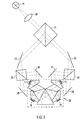
- FIG. 2 A possible Embodiment for the assembly of four fields into one The overall picture is shown in FIG. 2.
- the drawing files to be displayed are divided into four DMDs 15, 16, 17 and 18 are generated. To do this, the DMDs from a lighting unit illuminated, which is constructed so that a real light source over Intermediate images are mapped to four virtual images, with all light source images are identical.
- the partial images are generated in that light from a light source 19 is imaged on a first beam splitter 21 via an objective 20. This creates a virtual image of the light source.
- the light from a virtual image and light source is via two deflecting mirrors 22 and 23 to two further beam splitters 24 and 25 headed.
- the beam splitter creates additional virtual images.
- Their Beams are directed through the deflecting mirrors 26, 27, 28 and 29 Beam splitter complex 30 directed on which the DMDs are also arranged. in the Beam splitter complex, the illuminating beams are reflected on the DMDs which it then modulates according to the blid data of the respective field become.
- the light modulated and reflected by the DMD passes through the again Beam splitter complex and is deflected by this in such a way that that of the four DMDs reflected light is combined into a total beam in which the partial beams of the four drawing files without an overlap or a space lie side by side.
- This arrangement also ensures that all four illumination beam paths are exactly the same length, so that the Köhler'sche Beam path can be realized.
- FIG. 3 A possible complex from physical beam splitters, which achieves the object of the invention, is in FIG. 3 shown.
- the DMDs 34, 35, 36 and 37 generated partial images combined to form an overall image.
- An overall picture is then created on the photo paper, consisting of four side by side horizontal drawing files is constructed. This allows the original One-way resolution that would result from using only one DMD be quadrupled.
- this system can be expanded as required by adding more and more DMDs an additional level.
- the number of DMDs to be mapped can also be increased at the drawing level become. To do this, the DMDs must be spaced on one side of a beam splitter are set to each other, the distance being a multiple of a DMD length is. This creates gaps in the image caused by images of other DMDs Beam splitter pages are filled out.
Landscapes
- Physics & Mathematics (AREA)
- General Physics & Mathematics (AREA)
- Optics & Photonics (AREA)
- Engineering & Computer Science (AREA)
- Multimedia (AREA)
- Signal Processing (AREA)
- Spectroscopy & Molecular Physics (AREA)
- Exposure And Positioning Against Photoresist Photosensitive Materials (AREA)
- Projection-Type Copiers In General (AREA)
- Printers Or Recording Devices Using Electromagnetic And Radiation Means (AREA)
- Silver Salt Photography Or Processing Solution Therefor (AREA)
Applications Claiming Priority (2)
| Application Number | Priority Date | Filing Date | Title |
|---|---|---|---|
| DE19937417 | 1999-08-07 | ||
| DE19937417A DE19937417C1 (de) | 1999-08-07 | 1999-08-07 | Vorrichtung und Verfahren zum Belichten eines digitalen Bildes auf lichtempfindliches Material |
Publications (2)
| Publication Number | Publication Date |
|---|---|
| EP1081544A1 true EP1081544A1 (fr) | 2001-03-07 |
| EP1081544B1 EP1081544B1 (fr) | 2003-03-19 |
Family
ID=7917633
Family Applications (1)
| Application Number | Title | Priority Date | Filing Date |
|---|---|---|---|
| EP00113646A Expired - Lifetime EP1081544B1 (fr) | 1999-08-07 | 2000-06-28 | Dispositif et procédé pour projeter une image digitale sur un matériau photosensible |
Country Status (4)
| Country | Link |
|---|---|
| US (1) | US6498639B1 (fr) |
| EP (1) | EP1081544B1 (fr) |
| AT (1) | ATE235071T1 (fr) |
| DE (2) | DE19937417C1 (fr) |
Families Citing this family (3)
| Publication number | Priority date | Publication date | Assignee | Title |
|---|---|---|---|---|
| TWI298825B (en) * | 2002-06-12 | 2008-07-11 | Asml Netherlands Bv | Lithographic apparatus and device manufacturing method |
| CN100390600C (zh) | 2003-07-03 | 2008-05-28 | 汤姆森特许公司 | 使几束光束混合的照明系统 |
| DE102004053396A1 (de) * | 2004-11-05 | 2006-05-11 | Creative Computer Graphic Gmbh | Verfahren zum Belichten von Filmmaterial und Filmrecorder zur Durchführung des Verfahrens |
Citations (6)
| Publication number | Priority date | Publication date | Assignee | Title |
|---|---|---|---|---|
| US5105299A (en) * | 1990-12-31 | 1992-04-14 | Texas Instruments Incorporated | Unfolded optics for multiple row deformable mirror device |
| US5164854A (en) * | 1990-07-27 | 1992-11-17 | Victor Company Of Japan, Ltd. | Polarization converter for converting unpolarized light to linearly polarized light |
| US5704701A (en) * | 1992-03-05 | 1998-01-06 | Rank Brimar Limited | Spatial light modulator system |
| US5796526A (en) * | 1995-04-26 | 1998-08-18 | Texas Instruments Incorporated | Illumination optics for spatial light modulator |
| EP0922986A2 (fr) * | 1997-12-09 | 1999-06-16 | Unic View Ltd. | Projecteur d'images contrÔlable |
| EP1031874A1 (fr) * | 1999-02-05 | 2000-08-30 | Agfa-Gevaert AG | Dispositif et méthode d'exposition d'un image numérique sur matière photosensible |
Family Cites Families (7)
| Publication number | Priority date | Publication date | Assignee | Title |
|---|---|---|---|---|
| ATE178750T1 (de) * | 1991-01-25 | 1999-04-15 | Digital Projection Ltd | System mit raumlichem lichtmodulator für ein optisches farbausgangssignal |
| DE4211128C2 (de) * | 1992-04-03 | 1996-06-05 | Agfa Gevaert Ag | Verfahren zum Übertragen der Bildinformation einer Bildvorlage auf fotosensitives Material und Vorrichtung zur Durchführung des Verfahrens |
| JPH08262583A (ja) * | 1995-03-28 | 1996-10-11 | Fuji Photo Film Co Ltd | 分割画像露光方法 |
| US5636001A (en) * | 1995-07-31 | 1997-06-03 | Collier; John | Digital film camera and digital enlarger |
| JP3519853B2 (ja) * | 1996-02-28 | 2004-04-19 | 富士写真フイルム株式会社 | マイクロミラー式画像形成装置及びその管理方法 |
| EP0817157A3 (fr) * | 1996-06-28 | 1998-08-12 | Texas Instruments Incorporated | Des dispositifs d'affichage d'images |
| EP0933925A3 (fr) * | 1997-12-31 | 2002-06-26 | Texas Instruments Inc. | Photofinissage avec une grille de sources de lumière modulées |
-
1999
- 1999-08-07 DE DE19937417A patent/DE19937417C1/de not_active Expired - Fee Related
-
2000
- 2000-06-28 EP EP00113646A patent/EP1081544B1/fr not_active Expired - Lifetime
- 2000-06-28 DE DE50001477T patent/DE50001477D1/de not_active Expired - Fee Related
- 2000-06-28 AT AT00113646T patent/ATE235071T1/de not_active IP Right Cessation
- 2000-07-26 US US09/625,457 patent/US6498639B1/en not_active Expired - Fee Related
Patent Citations (7)
| Publication number | Priority date | Publication date | Assignee | Title |
|---|---|---|---|---|
| US5164854A (en) * | 1990-07-27 | 1992-11-17 | Victor Company Of Japan, Ltd. | Polarization converter for converting unpolarized light to linearly polarized light |
| US5105299A (en) * | 1990-12-31 | 1992-04-14 | Texas Instruments Incorporated | Unfolded optics for multiple row deformable mirror device |
| US5704701A (en) * | 1992-03-05 | 1998-01-06 | Rank Brimar Limited | Spatial light modulator system |
| US5796526A (en) * | 1995-04-26 | 1998-08-18 | Texas Instruments Incorporated | Illumination optics for spatial light modulator |
| EP0922986A2 (fr) * | 1997-12-09 | 1999-06-16 | Unic View Ltd. | Projecteur d'images contrÔlable |
| EP1031874A1 (fr) * | 1999-02-05 | 2000-08-30 | Agfa-Gevaert AG | Dispositif et méthode d'exposition d'un image numérique sur matière photosensible |
| DE19904750A1 (de) * | 1999-02-05 | 2000-08-31 | Agfa Gevaert Ag | Vorrichtung und Verfahren zum Belichten eines digitalen Bildes auf lichtempfindliches Material |
Also Published As
| Publication number | Publication date |
|---|---|
| ATE235071T1 (de) | 2003-04-15 |
| DE19937417C1 (de) | 2000-07-06 |
| US6498639B1 (en) | 2002-12-24 |
| EP1081544B1 (fr) | 2003-03-19 |
| DE50001477D1 (de) | 2003-04-24 |
Similar Documents
| Publication | Publication Date | Title |
|---|---|---|
| EP1016274B1 (fr) | Dispositif dans lequel une lumiere est dirigee sur une surface a partir d'une source lumineuse | |
| DE69614179T2 (de) | Anamorphisches Beleuchtungssystem für einen Lichtmodulator | |
| DE69730282T2 (de) | Projektionsgerät mit Mitteln zur Farbtrennung/-synthese | |
| DE102008051252B4 (de) | Projektionsobjektiv und Projektor | |
| DE69517220T2 (de) | Optisches Projektionssystem | |
| DE19833132B4 (de) | Vorrichtung und Verfahren zur Vereinigung von Lichtstrahlen mit Hilfe zweier flacher Platten mit einem dazwischenliegenden Luftspalt | |
| DE19733370C2 (de) | Vorrichtung und Verfahren zum Kopieren von Bilder auf lichtempfindliches Aufzeichnungsmaterial | |
| EP2294483A1 (fr) | Système de projection | |
| EP1145069A2 (fr) | Ensemble dans lequel de la lumiere provenant d'une source lumineuse est dirigee sur une surface | |
| DE2846696C2 (de) | Automatische Scharfeinstelleinrichtung für ein optisches Abbildungssystem | |
| DE4219851A1 (de) | Stereokamera | |
| EP1081544B1 (fr) | Dispositif et procédé pour projeter une image digitale sur un matériau photosensible | |
| DE10127620A1 (de) | Anordnung zum Projizieren eines mehrfarbigen Bildes auf eine Projektionsfläche | |
| EP1011005A2 (fr) | Unité de projection | |
| DE60006931T2 (de) | Bildprojektionssystem | |
| DE102004001389A1 (de) | Anordnung und Vorrichtung zur Minimierung von Randverfärbungen bei Videoprojektionen | |
| EP1031874A1 (fr) | Dispositif et méthode d'exposition d'un image numérique sur matière photosensible | |
| DE2412083B2 (de) | Optische strahlteileranordnung fuer eine farbfernsehkamera | |
| DE102021134130A1 (de) | Beleuchtungsvorrichtung zum Beleuchten einer Szene, Kamerasystem und Verfahren zum Beleuchten einer Szene | |
| DE102008029789B4 (de) | Projektionssystem | |
| DE102008029788B4 (de) | Projektionssystem | |
| DE19907345B4 (de) | Vorrichtung zum Abbilden eines als Raster von Bildpunkten darstellbaren Bildes auf einem Schirm | |
| EP3978983B1 (fr) | Système de projection | |
| DE102008063222A1 (de) | Verfahren und Vorrichtung zum Projizieren eines Bildes auf eine Projektionsfläche | |
| DE2736319A1 (de) | Verfahren zur homogenen ausleuchtung von objekt- und bildebenen |
Legal Events
| Date | Code | Title | Description |
|---|---|---|---|
| PUAI | Public reference made under article 153(3) epc to a published international application that has entered the european phase |
Free format text: ORIGINAL CODE: 0009012 |
|
| AK | Designated contracting states |
Kind code of ref document: A1 Designated state(s): AT BE CH CY DE DK ES FI FR GB GR IE IT LI LU MC NL PT SE |
|
| AX | Request for extension of the european patent |
Free format text: AL;LT;LV;MK;RO;SI |
|
| 17P | Request for examination filed |
Effective date: 20010907 |
|
| AKX | Designation fees paid |
Free format text: AT BE CH CY DE DK ES FI FR GB GR IE IT LI LU MC NL PT SE |
|
| 17Q | First examination report despatched |
Effective date: 20011114 |
|
| GRAH | Despatch of communication of intention to grant a patent |
Free format text: ORIGINAL CODE: EPIDOS IGRA |
|
| GRAH | Despatch of communication of intention to grant a patent |
Free format text: ORIGINAL CODE: EPIDOS IGRA |
|
| GRAA | (expected) grant |
Free format text: ORIGINAL CODE: 0009210 |
|
| AK | Designated contracting states |
Designated state(s): AT BE CH CY DE DK ES FI FR GB GR IE IT LI LU MC NL PT SE |
|
| PG25 | Lapsed in a contracting state [announced via postgrant information from national office to epo] |
Ref country code: NL Free format text: LAPSE BECAUSE OF FAILURE TO SUBMIT A TRANSLATION OF THE DESCRIPTION OR TO PAY THE FEE WITHIN THE PRESCRIBED TIME-LIMIT Effective date: 20030319 Ref country code: IE Free format text: LAPSE BECAUSE OF FAILURE TO SUBMIT A TRANSLATION OF THE DESCRIPTION OR TO PAY THE FEE WITHIN THE PRESCRIBED TIME-LIMIT Effective date: 20030319 Ref country code: GR Free format text: LAPSE BECAUSE OF FAILURE TO SUBMIT A TRANSLATION OF THE DESCRIPTION OR TO PAY THE FEE WITHIN THE PRESCRIBED TIME-LIMIT Effective date: 20030319 Ref country code: FI Free format text: LAPSE BECAUSE OF FAILURE TO SUBMIT A TRANSLATION OF THE DESCRIPTION OR TO PAY THE FEE WITHIN THE PRESCRIBED TIME-LIMIT Effective date: 20030319 |
|
| REG | Reference to a national code |
Ref country code: GB Ref legal event code: FG4D Free format text: NOT ENGLISH |
|
| REG | Reference to a national code |
Ref country code: CH Ref legal event code: EP |
|
| REG | Reference to a national code |
Ref country code: IE Ref legal event code: FG4D Free format text: GERMAN |
|
| REF | Corresponds to: |
Ref document number: 50001477 Country of ref document: DE Date of ref document: 20030424 Kind code of ref document: P |
|
| PG25 | Lapsed in a contracting state [announced via postgrant information from national office to epo] |
Ref country code: SE Free format text: LAPSE BECAUSE OF FAILURE TO SUBMIT A TRANSLATION OF THE DESCRIPTION OR TO PAY THE FEE WITHIN THE PRESCRIBED TIME-LIMIT Effective date: 20030619 Ref country code: DK Free format text: LAPSE BECAUSE OF FAILURE TO SUBMIT A TRANSLATION OF THE DESCRIPTION OR TO PAY THE FEE WITHIN THE PRESCRIBED TIME-LIMIT Effective date: 20030619 |
|
| PG25 | Lapsed in a contracting state [announced via postgrant information from national office to epo] |
Ref country code: PT Free format text: LAPSE BECAUSE OF FAILURE TO SUBMIT A TRANSLATION OF THE DESCRIPTION OR TO PAY THE FEE WITHIN THE PRESCRIBED TIME-LIMIT Effective date: 20030620 |
|
| PG25 | Lapsed in a contracting state [announced via postgrant information from national office to epo] |
Ref country code: LU Free format text: LAPSE BECAUSE OF NON-PAYMENT OF DUE FEES Effective date: 20030628 Ref country code: CY Free format text: LAPSE BECAUSE OF FAILURE TO SUBMIT A TRANSLATION OF THE DESCRIPTION OR TO PAY THE FEE WITHIN THE PRESCRIBED TIME-LIMIT Effective date: 20030628 Ref country code: AT Free format text: LAPSE BECAUSE OF NON-PAYMENT OF DUE FEES Effective date: 20030628 |
|
| PG25 | Lapsed in a contracting state [announced via postgrant information from national office to epo] |
Ref country code: MC Free format text: LAPSE BECAUSE OF NON-PAYMENT OF DUE FEES Effective date: 20030630 Ref country code: BE Free format text: LAPSE BECAUSE OF NON-PAYMENT OF DUE FEES Effective date: 20030630 |
|
| GBT | Gb: translation of ep patent filed (gb section 77(6)(a)/1977) |
Effective date: 20030718 |
|
| NLV1 | Nl: lapsed or annulled due to failure to fulfill the requirements of art. 29p and 29m of the patents act | ||
| ET | Fr: translation filed | ||
| PG25 | Lapsed in a contracting state [announced via postgrant information from national office to epo] |
Ref country code: ES Free format text: LAPSE BECAUSE OF FAILURE TO SUBMIT A TRANSLATION OF THE DESCRIPTION OR TO PAY THE FEE WITHIN THE PRESCRIBED TIME-LIMIT Effective date: 20030930 |
|
| REG | Reference to a national code |
Ref country code: IE Ref legal event code: FD4D Ref document number: 1081544E Country of ref document: IE |
|
| BERE | Be: lapsed |
Owner name: *AGFA-GEVAERT A.G. Effective date: 20030630 |
|
| PLBE | No opposition filed within time limit |
Free format text: ORIGINAL CODE: 0009261 |
|
| STAA | Information on the status of an ep patent application or granted ep patent |
Free format text: STATUS: NO OPPOSITION FILED WITHIN TIME LIMIT |
|
| 26N | No opposition filed |
Effective date: 20031222 |
|
| PGFP | Annual fee paid to national office [announced via postgrant information from national office to epo] |
Ref country code: CH Payment date: 20040616 Year of fee payment: 5 |
|
| PGFP | Annual fee paid to national office [announced via postgrant information from national office to epo] |
Ref country code: FR Payment date: 20040617 Year of fee payment: 5 |
|
| PGFP | Annual fee paid to national office [announced via postgrant information from national office to epo] |
Ref country code: GB Payment date: 20040618 Year of fee payment: 5 Ref country code: DE Payment date: 20040618 Year of fee payment: 5 |
|
| PG25 | Lapsed in a contracting state [announced via postgrant information from national office to epo] |
Ref country code: IT Free format text: LAPSE BECAUSE OF NON-PAYMENT OF DUE FEES Effective date: 20050628 Ref country code: GB Free format text: LAPSE BECAUSE OF NON-PAYMENT OF DUE FEES Effective date: 20050628 |
|
| PG25 | Lapsed in a contracting state [announced via postgrant information from national office to epo] |
Ref country code: LI Free format text: LAPSE BECAUSE OF NON-PAYMENT OF DUE FEES Effective date: 20050630 Ref country code: CH Free format text: LAPSE BECAUSE OF NON-PAYMENT OF DUE FEES Effective date: 20050630 |
|
| REG | Reference to a national code |
Ref country code: CH Ref legal event code: PUE Owner name: AGFAPHOTO GMBH Free format text: AGFA-GEVAERT AG#KAISER-WILHELM-ALLEE#51373 LEVERKUSEN (DE) -TRANSFER TO- AGFAPHOTO GMBH#KAISER-WILHELM-ALLEE#51373 LEVERKUSEN (DE) |
|
| REG | Reference to a national code |
Ref country code: CH Ref legal event code: PL |
|
| PG25 | Lapsed in a contracting state [announced via postgrant information from national office to epo] |
Ref country code: FR Free format text: LAPSE BECAUSE OF NON-PAYMENT OF DUE FEES Effective date: 20060228 |
|
| GBPC | Gb: european patent ceased through non-payment of renewal fee |
Effective date: 20050628 |
|
| REG | Reference to a national code |
Ref country code: FR Ref legal event code: ST Effective date: 20060228 |
|
| PG25 | Lapsed in a contracting state [announced via postgrant information from national office to epo] |
Ref country code: DE Free format text: LAPSE BECAUSE OF NON-PAYMENT OF DUE FEES Effective date: 20060601 |