EP1081755A2 - Méthode d'améliorer la qualité d'une couche dielectrique d'un dispositif semiconducteur - Google Patents
Méthode d'améliorer la qualité d'une couche dielectrique d'un dispositif semiconducteur Download PDFInfo
- Publication number
- EP1081755A2 EP1081755A2 EP00115048A EP00115048A EP1081755A2 EP 1081755 A2 EP1081755 A2 EP 1081755A2 EP 00115048 A EP00115048 A EP 00115048A EP 00115048 A EP00115048 A EP 00115048A EP 1081755 A2 EP1081755 A2 EP 1081755A2
- Authority
- EP
- European Patent Office
- Prior art keywords
- film
- sio
- heat treatment
- atmosphere
- quality improving
- Prior art date
- Legal status (The legal status is an assumption and is not a legal conclusion. Google has not performed a legal analysis and makes no representation as to the accuracy of the status listed.)
- Withdrawn
Links
Images


Classifications
-
- H—ELECTRICITY
- H10—SEMICONDUCTOR DEVICES; ELECTRIC SOLID-STATE DEVICES NOT OTHERWISE PROVIDED FOR
- H10P—GENERIC PROCESSES OR APPARATUS FOR THE MANUFACTURE OR TREATMENT OF DEVICES COVERED BY CLASS H10
- H10P14/00—Formation of materials, e.g. in the shape of layers or pillars
- H10P14/60—Formation of materials, e.g. in the shape of layers or pillars of insulating materials
- H10P14/65—Formation of materials, e.g. in the shape of layers or pillars of insulating materials characterised by treatments performed before or after the formation of the materials
- H10P14/6516—Formation of materials, e.g. in the shape of layers or pillars of insulating materials characterised by treatments performed before or after the formation of the materials of treatments performed after formation of the materials
- H10P14/6529—Formation of materials, e.g. in the shape of layers or pillars of insulating materials characterised by treatments performed before or after the formation of the materials of treatments performed after formation of the materials by exposure to a gas or vapour
-
- H—ELECTRICITY
- H10—SEMICONDUCTOR DEVICES; ELECTRIC SOLID-STATE DEVICES NOT OTHERWISE PROVIDED FOR
- H10P—GENERIC PROCESSES OR APPARATUS FOR THE MANUFACTURE OR TREATMENT OF DEVICES COVERED BY CLASS H10
- H10P14/00—Formation of materials, e.g. in the shape of layers or pillars
- H10P14/60—Formation of materials, e.g. in the shape of layers or pillars of insulating materials
- H10P14/63—Formation of materials, e.g. in the shape of layers or pillars of insulating materials characterised by the formation processes
- H10P14/6326—Deposition processes
- H10P14/6328—Deposition from the gas or vapour phase
- H10P14/6334—Deposition from the gas or vapour phase using decomposition or reaction of gaseous or vapour phase compounds, i.e. chemical vapour deposition
-
- H—ELECTRICITY
- H10—SEMICONDUCTOR DEVICES; ELECTRIC SOLID-STATE DEVICES NOT OTHERWISE PROVIDED FOR
- H10P—GENERIC PROCESSES OR APPARATUS FOR THE MANUFACTURE OR TREATMENT OF DEVICES COVERED BY CLASS H10
- H10P14/00—Formation of materials, e.g. in the shape of layers or pillars
- H10P14/60—Formation of materials, e.g. in the shape of layers or pillars of insulating materials
- H10P14/63—Formation of materials, e.g. in the shape of layers or pillars of insulating materials characterised by the formation processes
- H10P14/6326—Deposition processes
- H10P14/6342—Liquid deposition, e.g. spin-coating, sol-gel techniques or spray coating
-
- H—ELECTRICITY
- H10—SEMICONDUCTOR DEVICES; ELECTRIC SOLID-STATE DEVICES NOT OTHERWISE PROVIDED FOR
- H10P—GENERIC PROCESSES OR APPARATUS FOR THE MANUFACTURE OR TREATMENT OF DEVICES COVERED BY CLASS H10
- H10P14/00—Formation of materials, e.g. in the shape of layers or pillars
- H10P14/60—Formation of materials, e.g. in the shape of layers or pillars of insulating materials
- H10P14/66—Formation of materials, e.g. in the shape of layers or pillars of insulating materials characterised by the type of materials
- H10P14/668—Formation of materials, e.g. in the shape of layers or pillars of insulating materials characterised by the type of materials the materials being characterised by the deposition precursor materials
- H10P14/6681—Formation of materials, e.g. in the shape of layers or pillars of insulating materials characterised by the type of materials the materials being characterised by the deposition precursor materials the precursor containing a compound comprising Si
- H10P14/6684—Formation of materials, e.g. in the shape of layers or pillars of insulating materials characterised by the type of materials the materials being characterised by the deposition precursor materials the precursor containing a compound comprising Si the compound comprising silicon and oxygen
- H10P14/6686—Formation of materials, e.g. in the shape of layers or pillars of insulating materials characterised by the type of materials the materials being characterised by the deposition precursor materials the precursor containing a compound comprising Si the compound comprising silicon and oxygen the compound being a molecule comprising at least one silicon-oxygen bond and the compound having hydrogen or an organic group attached to the silicon or oxygen, e.g. a siloxane
-
- H—ELECTRICITY
- H10—SEMICONDUCTOR DEVICES; ELECTRIC SOLID-STATE DEVICES NOT OTHERWISE PROVIDED FOR
- H10P—GENERIC PROCESSES OR APPARATUS FOR THE MANUFACTURE OR TREATMENT OF DEVICES COVERED BY CLASS H10
- H10P14/00—Formation of materials, e.g. in the shape of layers or pillars
- H10P14/60—Formation of materials, e.g. in the shape of layers or pillars of insulating materials
- H10P14/69—Inorganic materials
- H10P14/692—Inorganic materials composed of oxides, glassy oxides or oxide-based glasses
- H10P14/6921—Inorganic materials composed of oxides, glassy oxides or oxide-based glasses containing silicon
- H10P14/69215—Inorganic materials composed of oxides, glassy oxides or oxide-based glasses containing silicon the material being a silicon oxide, e.g. SiO2
-
- H—ELECTRICITY
- H10—SEMICONDUCTOR DEVICES; ELECTRIC SOLID-STATE DEVICES NOT OTHERWISE PROVIDED FOR
- H10P—GENERIC PROCESSES OR APPARATUS FOR THE MANUFACTURE OR TREATMENT OF DEVICES COVERED BY CLASS H10
- H10P14/00—Formation of materials, e.g. in the shape of layers or pillars
- H10P14/60—Formation of materials, e.g. in the shape of layers or pillars of insulating materials
- H10P14/69—Inorganic materials
- H10P14/692—Inorganic materials composed of oxides, glassy oxides or oxide-based glasses
- H10P14/6921—Inorganic materials composed of oxides, glassy oxides or oxide-based glasses containing silicon
- H10P14/6922—Inorganic materials composed of oxides, glassy oxides or oxide-based glasses containing silicon the material containing Si, O and at least one of H, N, C, F or other non-metal elements, e.g. SiOC, SiOC:H or SiONC
-
- H—ELECTRICITY
- H10—SEMICONDUCTOR DEVICES; ELECTRIC SOLID-STATE DEVICES NOT OTHERWISE PROVIDED FOR
- H10P—GENERIC PROCESSES OR APPARATUS FOR THE MANUFACTURE OR TREATMENT OF DEVICES COVERED BY CLASS H10
- H10P95/00—Generic processes or apparatus for manufacture or treatments not covered by the other groups of this subclass
Definitions
- the present invention relates to a film quality improving method for an insulating film and a semiconductor device and, more particularly, a film quality improving method for an SiO 2 film for densifying the SiO 2 film by reducing impurities such as hydrocarbon, etc., which are contained in the SiO 2 film (insulating film) formed by the CVD (Chemical Vapor Deposition) method using a reaction gas containing TEOS (Tetraethoxysilane), and a semiconductor device.
- CVD Chemical Vapor Deposition
- heat treatment called annealing is applied to the insulating film.
- This heat treatment is performed for the purpose of improving the film quality of the insulating film.
- This heat treatment is performed by exposing the surface of the insulating film to the high temperature atmosphere containing an inert gas such as N 2 , etc.
- the heat treatment is performed by exposing the surface of the SiO 2 film (insulating film), which is formed by the CVD (Chemical Vapor Deposition) method using a reaction gas containing TEOS (Tetraethoxysilane), to the atmosphere containing steam.
- CVD Chemical Vapor Deposition
- TEOS Tetraethoxysilane
- steam or OH group dissociated from the steam enters into the inside of the SiO 2 film, then impurities such as hydrocarbon, etc. contained in the film are oxidized to desorb to the outside of the film.
- dangling bonds of Si (silicon) atoms contained in the film are replaced with SiO 2 bonds by a strong oxidizing tendency of the steam-containing atmosphere.
- the SiO 2 film whose film quality is close to the thermal oxide film can be obtained at the lower temperature compared with the heat treatment in the N 2 (nitrogen) atmosphere.
- the reason for this may be considered that the desorption of the above impurities and replacement of dangling bonds of the Si (silicon) atoms with the SiO 2 bonds can be achieved at the relatively low temperature. Therefore, since the heat treatment is performed at the lower temperature compared with the heat treatment in the N 2 (nitrogen) atmosphere, the device failure due to the heat treatment at the high temperature atmosphere is prevented.
- the film quality improvement reaches not only an upper layer portion of the SiO 2 film but also an almost 1.0 ⁇ m depth from a surface of the film. Therefore, the film quality improvement of the SiO 2 film that is formed in the deep trench, for example, can also be attained.
- FIGS.1A to 1G are sectional views showing the film quality Improving method for the insulating film according to the present embodiment.
- the film quality improving method for the insulating film according to the present invention will be explained with reference to steps of burying a STI (Shallow Trench Isolation) structure for device isolation as an example.
- STI Shallow Trench Isolation
- an SiN film 102 having an opening portion 102a is formed on a surface of a wafer (silicon single crystal) 101 that is a substrate.
- the dry etching is performed by using the SiN film 102 as a mask. Accordingly, the wafer (silicon single crystal) 101 located directly under the opening portion 102a is selectively etched, whereby a trench 103 is formed.
- a thermal oxide film 104 is formed in the trench 103 by exposing the wafer (silicon single crystal) 101 to the high temperature oxygen atmosphere.
- an SiO 2 film (insulating film) 105 is formed on an overall surface.
- This SiO 2 film 105 is formed by the atmospheric pressure CVD (atmospheric pressure Chemical Vapor Deposition) method containing TEOS and a high concentration O 3 in a reaction gas. It has been known that, if O 3 is added to the reaction gas at a relatively high concentration, the formed SiO 2 film 105 exhibits a surface flowability (also referred to as a "flow characteristic" hereinafter).
- TEOS is supplied to a chamber (not shown) by means of N 2 bubbling.
- the "TEOS/N 2 flow rate” on the fifth line of Table 1 is defined as the flow rate of N 2 used in this bubbling.
- the "N” in the unit “g/Nm 3 " on the sixth line of Table 1 is an abbreviation for "Normal (standard state)", and this unit “g/Nm 3 " is defined as a density in the standard state (0 °C, 1 atmospheric pressure).
- the impurities such as hydrocarbon, etc. are contained in the SiO 2 film 105 formed by the CVD method using the reaction gas containing TEOS. Such impurities exert a bad influence upon the characteristic of the semiconductor device. Therefore, the impurities such as hydrocarbon, etc. in the SiO 2 film 105 must be reduced to improve the film quality.
- a heat treatment is performed for the SiO 2 film 105. This heat treatment is carried out by exposing the surface of the SiO 2 film 105 to the steam-containing atmosphere.
- the oxygen and the hydrogen are supplied to the chamber to react with each other (hydrogen burning method).
- the heat treatment conditions temperature, oxygen flow rate, and hydrogen flow rate
- results obtained in the following are similar.
- the SiO 2 film 105 on the surface of the SiN film 102 is removed by polishing a surface of the SiO 2 film 105 by means of the CMP (Chemical Mechanical Polishing) method.
- CMP Chemical Mechanical Polishing
- the SiN film 102 formed on the surface of the wafer (silicon single crystal) 101 is removed, whereby the STI structure burying steps have been completed.
- the film quality of the SiO 2 film 105 which has been subjected to the heat treatment performed in the steam- containing atmosphere, as shown in FIG.1E, will be explained hereunder based on various measurements carried out by the inventors of the present invention. In particular, such film quality will be explained while comparing with the case where the heat treatment is performed by using N 2 (nitrogen).
- the inventors of the present invention investigated (I) a relationship between the heat treatment temperature and a wet etching rate ratio of the SiO 2 film 105 to the thermal oxide film, (II) a relationship between a depth from the surface of the SiO 2 film 105 and the wet etching rate ratio of the SiO 2 film 105 to the thermal oxide film at this depth, and (III) a relationship between the heat treatment temperature of the SiO 2 film 105 and change in the film thickness.
- the wet etching rate ratio of the SiO 2 film 105 to the thermal oxide film is defined as (wet etching rate of the SiO 2 film 105)/(wet etching rate of the thermal oxide film). This wet etching rate ratio serves as a criterion to decide to what extent the film quality of the SiO 2 film 105 is made close to that of the thermal oxide film.
- the wet etching rate ratio of the film is increased by them and therefore the wet etching rate ratio to the thermal oxide film is increased.
- the wet etching rate of the film comes close to that of the thermal oxide film and therefore the wet etching rate ratio to the thermal oxide film comes close to 1.
- the wet etching rate ratio to the thermal oxide film is closer to 1, a smaller amount of dangling bonds and the impurities are contained in the film, and therefore the film quality comes close to that of the thermal oxide film.
- the above heat treatment should be performed at low temperature as possible.
- FIG.2 is a graph showing the relationship between the heat treatment temperature and the wet etching rate ratio of the SiO 2 film 105 to the thermal oxide film.
- the film forming conditions of the SiO 2 film 105 at this time are given in Table 1.
- the 2 % hydrofluoric acid buffer solution is employed as the etchant.
- the results obtained when the heat treatment is performed in the N 2 (nitrogen) atmosphere are also depicted for comparison.
- the heat treatment conditions at this time are as shown in Table 2.
- the wet etching rate ratios are measured when the heat treatment temperature is set to 800 °C, 850 °C , 900 °C, 950 °C , 1000 °C , 1050 °C , and 1100 °C respectively.
- N 2 atmosphere Comp. example
- Steam-containing atmosphere Present invention
- N 2 flow rate 10.0 slm ------ H 2 flow rate ------ 6.0 slm O 2 flow rate ------ 8.0 slm Heat treatment
- the wet etching rate ratio cannot become smaller than 1.1 after the heat treatment of 1100 °C.
- the wet etching rate ratio becomes 1.06 , which is smaller than 1.1, after the heat treatment of 1000 °C which is lower than 1100 °C.
- the reason for this may be considered as follows. That is, if the steam is contained in the heat treatment atmosphere, an oxidizing tendency of the atmosphere is increased. Thus, because of the increased oxidizing tendency, the impurities such as hydrocarbon, etc. contained in the SiO 2 film 105 are oxidized to become lower molecular weight CO 2 . H 2 O, etc. and then easily desorb from the film. At the same time, dangling bonds of Si (silicon) atoms existing in the SiO 2 film 105 are perfectly replaced with SiO 2 bonds.
- the film quality of the SiO 2 film 105 can come much more closer to that of the thermal oxide film at the lower temperature than the case where the heat treatment is carried out in the N 2 atmosphere.
- the film quality improving method for the insulating film according to the present invention is applied to the SiO 2 film 105, the film quality of the SiO 2 film 105 can be made closer to that of the thermal oxide film at the lower temperature than the case where the heat treatment using the N 2 (nitrogen) is applied.
- the inventors of the present invention have found that, if a width of the trench 103 is narrow, the impurity 106 such as hydrocarbon, etc. is contained considerably in the inside of the SiO 2 film 105 buried in the trench 103 during the step of burying the SiO 2 film 105 (insulating film) into the trench 103 shown in FIG.1D.
- This reason may be considered such that, since the step of burying the SiO 2 film 105 into the trench 103 is completed in a short time if the width of the trench 103 is narrow, there is no time for the impurities such as hydrocarbon, etc., that are largely contained in the TEOS molecules constituting the oligomer to desorb from the film.
- the inventors of the present invention have applied the heat treatment to the SiO 2 film 105 in the N 2 (nitrogen) atmosphere.
- the inventors of the present invention have found that the impurities contained in the deep portion of the trench 103 as described above cannot be reduced sufficiently in the heat treatment using the N 2 (nitrogen). The reason for this may be considered such that, since the N 2 (nitrogen)is not oxidative, the impurity 106 cannot be sufficiently expelled to the outside of the film by the N 2 (nitrogen).
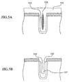
- FIG.5B is a sectional view showing experimental results obtained by the inventors of the present invention to verify that the impurities contained in the deep portion of the film cannot be sufficiently reduced in the heat treatment using the N 2 (nitrogen).
- FIG.5B shows the situation where the SiO 2 film 105 is exposed to the etchant such as HF (hydrofluoric acid), hydrofluoric acid buffer solution, etc. after the SiO 2 film 105 is subjected to the heat treatment using N 2 .
- the etchant such as HF (hydrofluoric acid), hydrofluoric acid buffer solution, etc.
- a void 107 is formed in the SiO 2 film 105 formed in the trench 103. This is because the etching rate of the SiO 2 film 105 where the impurity 106 is remained is increased higher than the SiO 2 film 105 where the impurity 106 is not remained and thus a portion of the SiO 2 film 105 where the impurity 106 is contained is apt to be etched.
- the impurities located not only in the surface layer of the film but also in the deep portion of the film can be reduced by the heat treatment of the SiO 2 film 105.
- the inventors of the present invention have examined a relationship between a depth from the surface of the SiO 2 film 105 and the wet etching rate ratio of the SiO 2 film 105 to the thermal oxide film at this depth.
- FIG.3 is a graph showing a relationship between the depth from the surface of the SiO 2 film 105 and the wet etching rate ratio of the SiO 2 film 105 to the thermal oxide film at this depth.
- the wet etching rate ratio of the SiO 2 film 105 to the thermal oxide film is substantially constant in the depth range of 0.0 ⁇ m to 1.0 ⁇ m from the surface of the film. This indicates that the film quality improving effect is attained not only in the surface layer portion of the film, but also attained in the whole of the film uniformly.
- the film quality improving method for the insulating film of the present invention it can be expected the film quality in the deeper portion of the SiO 2 film 105 can be improved compared with the heat treatment using the N 2 (nitrogen).
- the insulating film such as the SiO 2 film 105, etc. is thermally shrunken by the heat treatment. This is because the insulating film is densified by the heat treatment and thus the film is shrunken by an amount of increase of the density.
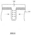
- FIG.6 shows the situation of such shrinkage when employing the heat treatment using N 2 .
- the SiO 2 film 105 is shrunken along the direction indicated by solid line arrows in FIG.6.
- the tensile stress is applied to the wafer (silicon single crystal) 101 along the direction indicated by broken line arrows in FIG.6 with the shrinkage of the SiO 2 film 105.
- This tensile stress causes the crystal defect in the wafer (silicon single crystal) 101 and thus causes the device failure.
- the inventors of the present invention have examined how the film thickness of the SiO 2 film 105 is changed by the film quality improving method for the insulating film according to the present invention.
- FIG.4 is a graph showing a relationship between the heat treatment temperature of the SiO 2 film 105 and change in the film thickness.
- the results obtained when the heat treatment is performed in the N 2 atmosphere are also depicted for the sake of comparison.
- the reduction of the film thickness of about 30 nm to 50 nm is found.
- the reduction of the film thickness of about 1.5 nm is found at 950 °C, and the increase of the film thickness of about 10 nm is found at 1100 °C at which the change in the film thickness is maximum.
- the change in the film thickness is monotonously reduced as the heat treatment temperature is increased. This is because the film is densified with the increase of the heat treatment temperature and thus the film is shrunken by an amount of the increase of the density.
- the change in the film thickness is monotonously increased with the increase of the heat treatment temperature.
- Si (silicon) layers on the side wall portion and the bottom portion of the trench 103 are thermally oxidized by the strong oxidizing tendency of the steam-containing atmosphere to generate new SiO 2 .
- the increase of the film thickness of the SiO 2 film 105 due to the newly generated SiO 2 is larger than the reduction of the film thickness due to the desorption of the impurities such as hydrocarbon, etc.
- the overall film thickness of the SiO 2 film 105 is increased.
- an amount of the newly generated SiO 2 as explained above is increased if the heat treatment temperature is increased, the change of the film thickness is monotonously increased as a function of the heat treatment temperature.
- the change of the film thickness of the SiO 2 film 105, to which the film quality improving method for the insulating film according to the present invention is applied is smaller than zero. It may be considered as the reason for this that the reduction of the film thickness due to the desorption of the impurities is larger than the increase of the film thickness due to the newly generated SiO 2 at this temperature or less.
- the change of the film thickness of the SiO 2 film 105 becomes almost zero. It may be considered as the reason for this that the reduction of the film thickness due to the desorption of the impurities such as hydrocarbon, etc. and the increase of the film thickness due to the newly generated SiO 2 cancel each other and thus the overall film thickness of the SiO 2 film 105 is not changed.
- the improving method of the present invention is performed at the temperature of about 1000°C
- the change in the film thickness of the SiO 2 film 105 due to the heat treatment can be reduced compared with the heat treatment in the N 2 (nitrogen) atmosphere.
- the film quality improving method according to the present invention is applied to the SiO 2 film which is formed by using the CVD method using TEOS, but the present invention should not be limited to the above. That is, the film quality improving method according to the present invention can also be applied to the silicon oxide film formed by any film forming method.
- the film quality improving method for the insulating film according to the present invention was explained while taking the steps of burying the STI structure of the semiconductor device as an example.
- the scope in which the present invention can be applied should not be limited to the above.
- the present invention can be applied to the interlayer insulating film of the semiconductor device, etc.
- the film quality improving method for the insulating film according to the present invention was explained in the above, the insulating film whose quality is improved by using the improving method of the present invention may be applied to the semiconductor device.
- the impurities contained in the insulating film is reduced sufficiently, such a problem seldom occurs that the characteristics of the device are harmfully affected by the impurities.
- such another problem is hard to occur that the device failure of the semiconductor device is caused by the tensile stress of the insulating film due to the heat treatment.
- the film quality improving method for the insulating film of the present invention following advantages can be achieved by applying the heat treatment in the steam-containing atmosphere to the SiO 2 film, which is formed by the CVD method using the reaction gas containing TEOS.
- the insulating film that is subjected to the film quality improving method for the insulating film according to the present invention is applied to the semiconductor device, the number of impurities contained in the insulating film as well as the tensile stress caused by the heat treatment can be satisfactorily reduced. As a result, the semiconductor device in which the device failure is seldom caused can be provided.
Landscapes
- Formation Of Insulating Films (AREA)
- Internal Circuitry In Semiconductor Integrated Circuit Devices (AREA)
Applications Claiming Priority (2)
| Application Number | Priority Date | Filing Date | Title |
|---|---|---|---|
| JP24772799A JP3245136B2 (ja) | 1999-09-01 | 1999-09-01 | 絶縁膜の膜質改善方法 |
| JP24772799 | 1999-09-01 |
Publications (2)
| Publication Number | Publication Date |
|---|---|
| EP1081755A2 true EP1081755A2 (fr) | 2001-03-07 |
| EP1081755A3 EP1081755A3 (fr) | 2001-11-07 |
Family
ID=17167784
Family Applications (1)
| Application Number | Title | Priority Date | Filing Date |
|---|---|---|---|
| EP00115048A Withdrawn EP1081755A3 (fr) | 1999-09-01 | 2000-07-26 | Méthode d'améliorer la qualité d'une couche dielectrique d'un dispositif semiconducteur |
Country Status (5)
| Country | Link |
|---|---|
| US (2) | US6548426B1 (fr) |
| EP (1) | EP1081755A3 (fr) |
| JP (1) | JP3245136B2 (fr) |
| KR (1) | KR100394504B1 (fr) |
| TW (1) | TW471072B (fr) |
Families Citing this family (9)
| Publication number | Priority date | Publication date | Assignee | Title |
|---|---|---|---|---|
| DE60226022D1 (de) | 2001-04-24 | 2008-05-21 | Nissan Chemical Ind Ltd | Verfahren zur herstellung eines dicken films auf basis von siliciumdioxid |
| JP4342895B2 (ja) * | 2003-10-06 | 2009-10-14 | 東京エレクトロン株式会社 | 熱処理方法及び熱処理装置 |
| JP4285184B2 (ja) * | 2003-10-14 | 2009-06-24 | 東京エレクトロン株式会社 | 成膜方法及び成膜装置 |
| JP2005203730A (ja) | 2003-12-18 | 2005-07-28 | Seiko Epson Corp | 絶縁膜、半導体素子、電子デバイスおよび電子機器 |
| JP4649899B2 (ja) * | 2004-07-13 | 2011-03-16 | パナソニック株式会社 | 半導体記憶装置およびその製造方法 |
| JP4764988B2 (ja) * | 2004-07-29 | 2011-09-07 | 富士電機株式会社 | 絶縁ゲート型電界効果トランジスタの製造方法 |
| EP2024532A4 (fr) * | 2006-05-30 | 2014-08-06 | Applied Materials Inc | Depot chimique en phase vapeur de dioxyde de silicium a ecoulement de haute qualite a partir d'un precurseur contenant du silicium et d'oxygene atomique |
| JP2014011234A (ja) | 2012-06-28 | 2014-01-20 | Tokyo Electron Ltd | シリコン酸化膜の形成方法およびその形成装置 |
| JP6013313B2 (ja) * | 2013-03-21 | 2016-10-25 | 東京エレクトロン株式会社 | 積層型半導体素子の製造方法、積層型半導体素子、及び、その製造装置 |
Family Cites Families (18)
| Publication number | Priority date | Publication date | Assignee | Title |
|---|---|---|---|---|
| KR0165856B1 (ko) | 1988-05-17 | 1999-02-01 | 윌리엄 에이취 오우웬 | 침착 터널링 산화물의 제조방법 |
| US5525550A (en) | 1991-05-21 | 1996-06-11 | Fujitsu Limited | Process for forming thin films by plasma CVD for use in the production of semiconductor devices |
| KR930010401B1 (ko) | 1991-06-17 | 1993-10-23 | 삼성전자 주식회사 | 접촉구 형성후의 bpsg 리플로우 방법 |
| JP3113957B2 (ja) | 1992-11-17 | 2000-12-04 | 日本電信電話株式会社 | 半導体装置 |
| JP3416163B2 (ja) * | 1992-01-31 | 2003-06-16 | キヤノン株式会社 | 半導体基板及びその作製方法 |
| JPH05304147A (ja) | 1992-04-27 | 1993-11-16 | Fujitsu Ltd | 半導体装置の製造方法 |
| US5561082A (en) * | 1992-07-31 | 1996-10-01 | Kabushiki Kaisha Toshiba | Method for forming an electrode and/or wiring layer by reducing copper oxide or silver oxide |
| JPH06151416A (ja) | 1992-11-09 | 1994-05-31 | Hitachi Ltd | 半導体装置及びその製造方法 |
| US5492858A (en) | 1994-04-20 | 1996-02-20 | Digital Equipment Corporation | Shallow trench isolation process for high aspect ratio trenches |
| KR960002520A (ko) * | 1994-06-20 | 1996-01-26 | 김주용 | 반도체 소자의 층간 절연막 형성방법 |
| US5530293A (en) * | 1994-11-28 | 1996-06-25 | International Business Machines Corporation | Carbon-free hydrogen silsesquioxane with dielectric constant less than 3.2 annealed in hydrogen for integrated circuits |
| KR970052909A (ko) | 1995-12-26 | 1997-07-29 | 김광호 | 반도체 장치의 평탄화 방법 |
| JP2980052B2 (ja) * | 1997-03-31 | 1999-11-22 | 日本電気株式会社 | 半導体装置の製造方法 |
| JPH10284484A (ja) | 1997-04-04 | 1998-10-23 | Sony Corp | シリコン酸化膜の形成方法 |
| JPH10335325A (ja) * | 1997-05-29 | 1998-12-18 | Seiko Epson Corp | 酸化硅素膜形成方法 |
| JPH10340909A (ja) * | 1997-06-06 | 1998-12-22 | Hitachi Ltd | 半導体集積回路装置の製造方法 |
| JPH113936A (ja) * | 1997-06-13 | 1999-01-06 | Nec Corp | 半導体装置の製造方法 |
| JPH11233508A (ja) | 1998-02-13 | 1999-08-27 | Sony Corp | 絶縁膜の形成方法 |
-
1999
- 1999-09-01 JP JP24772799A patent/JP3245136B2/ja not_active Expired - Fee Related
-
2000
- 2000-07-24 TW TW089114713A patent/TW471072B/zh not_active IP Right Cessation
- 2000-07-25 US US09/625,355 patent/US6548426B1/en not_active Expired - Fee Related
- 2000-07-26 EP EP00115048A patent/EP1081755A3/fr not_active Withdrawn
- 2000-08-23 KR KR10-2000-0048809A patent/KR100394504B1/ko not_active Expired - Fee Related
-
2003
- 2003-01-02 US US10/334,971 patent/US20030181062A1/en not_active Abandoned
Also Published As
| Publication number | Publication date |
|---|---|
| KR100394504B1 (ko) | 2003-08-14 |
| EP1081755A3 (fr) | 2001-11-07 |
| JP3245136B2 (ja) | 2002-01-07 |
| JP2001077105A (ja) | 2001-03-23 |
| KR20010030117A (ko) | 2001-04-16 |
| US20030181062A1 (en) | 2003-09-25 |
| US6548426B1 (en) | 2003-04-15 |
| TW471072B (en) | 2002-01-01 |
Similar Documents
| Publication | Publication Date | Title |
|---|---|---|
| US6719012B2 (en) | Method of forming trench isolation regions | |
| US6277706B1 (en) | Method of manufacturing isolation trenches using silicon nitride liner | |
| KR100788183B1 (ko) | 유동성 산화물 필름 중의 탄소를 제거하기 위한 증착후오존 처리방법 | |
| US5726090A (en) | Gap-filling of O3 -TEOS for shallow trench isolation | |
| US8221642B2 (en) | Methods for removing dielectric materials | |
| US7033945B2 (en) | Gap filling with a composite layer | |
| US6271153B1 (en) | Semiconductor processing method and trench isolation method | |
| EP1081755A2 (fr) | Méthode d'améliorer la qualité d'une couche dielectrique d'un dispositif semiconducteur | |
| JP2001085511A (ja) | 素子分離方法 | |
| US6992020B2 (en) | Method of fabricating semiconductor device | |
| US6323101B1 (en) | Semiconductor processing methods, methods of forming silicon dioxide methods of forming trench isolation regions, and methods of forming interlevel dielectric layers | |
| KR100334245B1 (ko) | 소자분리영역의 형성 방법 | |
| KR100403628B1 (ko) | 반도체 장치의 소자분리 방법 | |
| KR100297171B1 (ko) | 반도체소자의소자분리방법 | |
| KR100492790B1 (ko) | 반도체소자의소자분리절연막형성방법 | |
| KR20010109544A (ko) | 반도체 장치의 소자분리막 형성 방법 | |
| KR20040001874A (ko) | 반도체 소자의 트렌치형 소자분리막 형성방법 | |
| KR20020002161A (ko) | 반도체 소자분리막 형성방법 |
Legal Events
| Date | Code | Title | Description |
|---|---|---|---|
| PUAI | Public reference made under article 153(3) epc to a published international application that has entered the european phase |
Free format text: ORIGINAL CODE: 0009012 |
|
| AK | Designated contracting states |
Kind code of ref document: A2 Designated state(s): DE FR GB NL Kind code of ref document: A2 Designated state(s): AT BE CH CY DE DK ES FI FR GB GR IE IT LI LU MC NL PT SE |
|
| AX | Request for extension of the european patent |
Free format text: AL;LT;LV;MK;RO;SI |
|
| PUAL | Search report despatched |
Free format text: ORIGINAL CODE: 0009013 |
|
| AK | Designated contracting states |
Kind code of ref document: A3 Designated state(s): AT BE CH CY DE DK ES FI FR GB GR IE IT LI LU MC NL PT SE |
|
| AX | Request for extension of the european patent |
Free format text: AL;LT;LV;MK;RO;SI |
|
| 17P | Request for examination filed |
Effective date: 20011211 |
|
| AKX | Designation fees paid |
Free format text: DE FR GB NL |
|
| STAA | Information on the status of an ep patent application or granted ep patent |
Free format text: STATUS: THE APPLICATION IS DEEMED TO BE WITHDRAWN |
|
| 18D | Application deemed to be withdrawn |
Effective date: 20060425 |