EP1081765B1 - Circuit intégré dans un substrat protégé contre une inversion de tension - Google Patents
Circuit intégré dans un substrat protégé contre une inversion de tension Download PDFInfo
- Publication number
- EP1081765B1 EP1081765B1 EP00109566A EP00109566A EP1081765B1 EP 1081765 B1 EP1081765 B1 EP 1081765B1 EP 00109566 A EP00109566 A EP 00109566A EP 00109566 A EP00109566 A EP 00109566A EP 1081765 B1 EP1081765 B1 EP 1081765B1
- Authority
- EP
- European Patent Office
- Prior art keywords
- well
- circuit arrangement
- semiconductor switch
- substrate
- arrangement according
- Prior art date
- Legal status (The legal status is an assumption and is not a legal conclusion. Google has not performed a legal analysis and makes no representation as to the accuracy of the status listed.)
- Expired - Lifetime
Links
Images



Classifications
-
- H—ELECTRICITY
- H10—SEMICONDUCTOR DEVICES; ELECTRIC SOLID-STATE DEVICES NOT OTHERWISE PROVIDED FOR
- H10D—INORGANIC ELECTRIC SEMICONDUCTOR DEVICES
- H10D89/00—Aspects of integrated devices not covered by groups H10D84/00 - H10D88/00
- H10D89/60—Integrated devices comprising arrangements for electrical or thermal protection, e.g. protection circuits against electrostatic discharge [ESD]
- H10D89/601—Integrated devices comprising arrangements for electrical or thermal protection, e.g. protection circuits against electrostatic discharge [ESD] for devices having insulated gate electrodes, e.g. for IGFETs or IGBTs
-
- H—ELECTRICITY
- H02—GENERATION; CONVERSION OR DISTRIBUTION OF ELECTRIC POWER
- H02H—EMERGENCY PROTECTIVE CIRCUIT ARRANGEMENTS
- H02H11/00—Emergency protective circuit arrangements for preventing the switching-on in case an undesired electric working condition might result
- H02H11/002—Emergency protective circuit arrangements for preventing the switching-on in case an undesired electric working condition might result in case of inverted polarity or connection; with switching for obtaining correct connection
- H02H11/003—Emergency protective circuit arrangements for preventing the switching-on in case an undesired electric working condition might result in case of inverted polarity or connection; with switching for obtaining correct connection using a field effect transistor as protecting element in one of the supply lines
Definitions
- the present invention relates to a reverse polarity protected integratable circuit in a first conductivity type substrate having first and second opposing major surfaces.
- the substrate has at least one first well of the second conductivity type, which contains at least one field-effect-controllable semiconductor component.
- the first tub reaches to the first main page.
- Monolithically integrated circuit arrangements are realized in a semiconductor substrate which may be n-type or p-type.
- the semiconductor elements of the integrated circuit device are provided in a p-well disposed in the substrate.
- the entire circuit arrangement can be provided either in a single well or in a plurality of wells in the substrate.
- power components are also realized together with logic components in a substrate.
- the logic components are then isolated from the power device.
- electrical isolation occurs through the pn junction formed by the p-well and the substrate.
- the n-type substrate must then have a higher potential than the p-type wells.
- self-insulating technology In this case, one speaks of a so-called self-insulating technology.
- the electrical contacts of the logic devices are located on the major surface of the substrate to which the well in which the logic devices are integrated extends. This main page will be referred to as the first main area. If additionally a power component is provided, this is often realized in a vertical form, ie the second main surface of the substrate is usually connected to a high supply potential.
- the above arrangement described by way of example may represent a smart semiconductor switch. Such an arrangement is described, for example, in document DE 44 23 733 A1.
- the basic circuit arrangement of a smart cruffleerschalters is shown in Figure 4.
- the figure shows a so-called high-side switch. This is characterized by the fact that the semiconductor switch 21, which is shown in the present figure as a MOSFET, drain connected to a high supply potential V bb . This is connected to a supply potential terminal 7.
- a load 15 is connected in series, whose non-connected to the MOSFET 7 terminal is connected to a reference potential terminal 8b, which is usually the ground potential.
- the MOSFET 21 is controlled by a drive circuit 19, which contains all elements for controlling the high-side switch. These include z. B. a charge pump with, the gate voltage of the MOSFET can be set to a value which is higher than the supply voltage V bb .
- a semiconductor switch which is connected between the gate and the source of the MOSFET 21 and with which the MOSFET 21 can be turned off.
- the drive circuit 19 includes at least one transistor in the gate lead, with which the charge current for the gate-source capacitance of the MOSFET 21 can be controlled.
- the structure of the functional block is known per se and therefore not the subject of the invention.
- the drive circuit 19 is further connected via a resistor 17 to a reference potential terminal 8a. It is connected via a control terminal and is further connected to the supply potential terminal 7, which is usually located on the second main surface of the substrate.
- the elements necessary for driving the semiconductor switch 21 are usually integrated together in a first well 2b, which is provided in a substrate 1 (indicated schematically).
- the well 2b is usually connected to the source terminal S of the MOSFET 21.
- further wells 2c, 2d may be provided which include, for example, an overtemperature protection or overcurrent detection.
- the tubs 2b, 2c, 2d are electrically separated from each other.
- the reference potential terminals 8a, 8b in the case of the present circuit arrangement, have no direct electrical connection to one another.
- a condition critical for the circuit arrangement exists when the potential applied to the supply potential terminal 7 drops below that at the reference potential terminal 8a, 8b, ie. H. there is a reverse polarity.
- a current can flow from the reference potential terminal 8 b to the supply potential terminal 7 via the reverse-sequence diode which is technologically conditioned in the MOSFET 21.
- It is a high power dissipation implemented in the MOSFET 21, which can lead to destruction of the smart semiconductor switch.
- the reverse polarity is equally critical for the drive circuit 19, since the self-isolation no longer works and there is a high thermal power loss is implemented. In order to prevent thermal destruction of the integrated circuit arrangement, it is therefore necessary in a Verpolfall 13, Kunststoffn the MOSFET 21, so that a current through the technologically related reverse diode is avoided.
- the object of the present invention is therefore to provide a circuit arrangement which prevents failure of the circuit arrangement in a Verpolfall.
- the circuit arrangement should also be technologically integrable.
- the invention is based on the recognition that a first semiconductor switch, connected in series with a load between two supply potential terminals, must be conductively controlled in a coil.
- the drive circuit must provide the first semiconductor switch at its control terminal a voltage available, which is sufficient to turn this conductive. If the drive circuit is realized in a self-insulating technology in a substrate, then in a Verpolfall parasitic elements, for. B. bipolar transistors formed between the substrate of the first conductivity type, a first well of the second conductivity type therein and integrated therein elements containing regions of the first conductivity type are formed, which oppose the desired operation.
- the drive circuit 19 is in Verpolfall not able to provide the control terminal of the first semiconductor switch, a voltage which is sufficient to switch the first semiconductor switch conductive.
- the impairment may be due to parasitic elements in Verpolfall also other functions, such. B. a temperature monitoring or overload protection are disturbed.
- the second conductivity-type second well having the first conductivity-type region formed therein together with the substrate in a coil form another parasitic bipolar transistor, the collector of which drives the bipolar transistors in the at least one well and eliminates their negative effects in the coil.
- the functionality of the functions provided in a drive circuit can also be maintained in the field of polarity, since the base of the parasitic bipolar transistor in the first well is short-circuited via the further parasitic bipolar transistor.
- the second well is connected to a power source, which normally provides no power and which in Verpolfall provides a stream. In this way it is ensured that the parasitic bipolar transistors are driven in the first well only in a Verpolfall. In normal operation, there is no influence by the structure formed with the second well.
- the first well it is advantageous to refer the first well to a defined potential via a resistor. In this case, a "float" of the first tub is avoided. Floating the first tub could adversely affect the functionality of the components therein during normal operation.
- the integrable circuit arrangement according to the invention has a plurality of first wells, wherein elements for driving the first semiconductor switch are provided in one of the first wells.
- elements for driving the first semiconductor switch are provided in one of the first wells.
- the current source connected to the second well may be implemented as a resistor, which is also connected to the output of the circuit arrangement.
- a MOS diode is provided in a further of the first wells.
- the MOS diode and a resistor are connected in series between the control terminal of the first semiconductor switch and a reference potential terminal.
- a polarity reversal protection for the first semiconductor switch can be realized in a simple manner. In this case, a control of the first semiconductor switch in a Verpolfall is guaranteed regardless of a drive circuit.
- a second and a third semiconductor switch is advantageously provided in the first well, in which the MOS diode is integrated. These bring in normal operation the connection point between the diode and the resistor to the potential of the output terminal.
- Figure 1 shows in cross section a section of the integrated circuit arrangement according to the invention.
- a substrate 1 which is n-conductive in the present example, a first well 2b is arranged, which extends to the first main surface I of the substrate 1.
- the first well 2b is of the conductivity type opposite to the substrate, ie p-type in the present embodiment.
- two semiconductor switches 13 are shown.
- the semiconductor switches 13 are shown as lateral field-effect-controlled components. These have a control terminal 13G, an n-type source region 13S and a likewise n-type drain region 13D.
- first well 2b for example, those components are integrated, which serve for the direct control of a first semiconductor switch, which is connected in series with a load.
- the first well 2b is connected to an output terminal 14, which is the connection point between the load and the first semiconductor switch.
- the second main surface II is connected to a supply potential terminal 7, to which a high supply potential V bb is normally applied.
- the lowest supply potential, -V bb is present at the supply potential terminal 7.
- a parasitic bipolar transistor 10 is formed between the n-type substrate 1, the p-type first well 2b, and the drain and source regions 13D, 13S of the semiconductor switch 13, respectively.
- the first well 2b is connected to a resistor 6, which may for example be designed as an external resistor.
- the resistor 6 serves to keep the first well 2b at a fixed potential.
- the base of the parasitic bipolar transistor 10 obtained via the resistor 6 control current, so that this would be turned on. The correct operation of the semiconductor switch 13 would not be guaranteed in this case.
- a second well 3b which is p-type.
- the second well 3b extends to the first main surface I of the substrate 1.
- a region 4 is provided, which is n-type and extends to the first main surface I.
- the region 4 is electrically connected to the p-type first well 2b. This can be done for example via a metallization. In the present example, this is arranged adjacent to the first well 2b. However, this is not absolutely necessary. Relevant is an electrical connection between the area 4 and the first tub, so that the local arrangement plays a minor role.
- the second well 3b is further connected via a resistor 9.
- the resistor 9 is also connected to the output terminal 14. However, if there is no connection of the p-type first well with the output terminal 14, the resistor 9 is to be connected to a reference potential terminal. This would be the case, for example, for logical functions that do not serve to drive the first semiconductor switch.
- a further parasitic bipolar transistor 11 is formed.
- the collector of the parasitic bipolar transistor 11 is connected to the base of the parasitic bipolar transistor 10 in the first well 2b.
- the output terminal 14 is in this case (via a load) to a high potential, ie it provides via the resistor 9 to the bipolar transistor 11, a control current, which in turn drives the base of the parasitic bipolar transistor 10.
- the dysfunctional Effect of the bipolar transistor 10 in the first well 2b can be prevented in this way.
- FIG. 2 shows a variation of the integrated circuit arrangement described in FIG.
- a MOS diode 12 is provided in a first well 2a, which is not identical to the first well 2b of Figure 1, a MOS diode 12 is provided.
- the source terminal 12S of the MOS diode 12 is connected to the gate terminal 12G. This is also connected via an external resistor 16 to a reference potential terminal 8a.
- the control terminal of a first semiconductor switch 21 is connected via a resistor 18.
- Adjacent to the first well 2a, a second well 3a is provided, which is introduced into the substrate 1.
- An n-conducting region 4 is also provided on the first main surface I. The region 4 is connected to the first well 2a via an electrical connection.
- the second tub 3a and the second tub 3b of Figure 1 are not identical. There is also no electrical connection between these two areas.
- the section shown in Figure 2 of the circuit arrangement according to the invention allows a reverse polarity protection for a semiconductor switch in a simple manner.
- a reverse polarity of the bipolar transistor 11 controls the bipolar transistor 10 in the first well 2a, so that a sufficiently high voltage can be applied to the control terminal of the first semiconductor switch to conduct it in the event of reverse polarity.
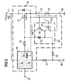
- FIG. 3 shows the basic electrical equivalent circuit of the polarity reversal protection according to the invention for the high-side semiconductor switch already described above.
- the first semiconductor switch 21 which is designed in the present example as a MOSFET, is on the drain side with connect the supply to the supply 7.
- the connection terminal between the source terminal and the load 15 constitutes an output terminal 14.
- the MOSFET 21 is controlled via a drive circuit 19.
- a gate charge resistor 18 is provided.
- the drive circuit 19 is controlled via a control terminal 20.
- the areas 2b to 2d shown by dashed lines in the drive circuit 19 are intended to indicate different functional blocks of an intelligent semiconductor switch, which are each realized in different first wells 2b, 2c or 2d.
- the first well 2b combines the necessary to control the gate terminal G components. As shown in FIG. 1, the first well 2b is accommodated in the substrate 1, which is connected to the output terminal 14.
- the drive circuit 19 is further connected via a resistor 17 to a reference potential terminal 8a.
- the reference potential terminals 8a and 8b have no electrical connection to each other.
- the polarity reversal protection of the present invention consists of a diode 12 and a resistor 16, which are connected in series between the gate G and the reference potential terminal 8a. On the cathode side, the diode 12 is connected to the gate G of the MOSFET 21.
- the polarity reversal protection according to the invention further comprises a second and a third semiconductor switch 23, 24 whose load paths are connected in series between the supply potential terminal 7 and the output terminal 14.
- the second semiconductor switch 23 is realized as a MOSFET, while the third semiconductor switch 24 is designed as a bipolar transistor.
- the collector of the bipolar transistor 24 is connected to the supply potential terminal 7.
- the emitter of the bipolar transistor 24 is connected on the one hand to the drain of the MOSFET 23 and on the other hand to the connection point of the resistor 16 and the diode 12.
- the base terminal of the bipolar transistor 24 is connected to the source terminal of the MOSFET 23 connected.
- the gate of the MOSFET 23 is connected to the supply potential terminal 7.
- the gate of the MOSFET 21 is a diode voltage above the reference potential 8a. Thus, it is ensured that the MOSFET 21 is turned on in a Verpolfall.
- the semiconductor switches 23, 24 ensure that the connection point between the diode 12 and the resistor 16 is at the potential of the output terminal 14. Thus, the function of the drive circuit 19 is not affected in normal operation.
- the MOSFET 23 is conductively controlled in normal operation, since the potential at its gate is above the potential of the source terminal.
Landscapes
- Semiconductor Integrated Circuits (AREA)
- Metal-Oxide And Bipolar Metal-Oxide Semiconductor Integrated Circuits (AREA)
Claims (9)
- Circuit protégé contre une inversion de tension et intégré dans un substrat (1) d'un premier type de conductibilité avec une première surface principale (I) et une deuxième surface principale (II) opposée à la première, avec:- au moins une première cuvette (2a-2d) du deuxième type de conductibilité, qui comprend au moins un élément semi-conducteur (12, 13, 23, 24) pouvant être commandé par effet de champ, et qui est disposée sur la première surface principale (I) de façon à pénétrer dans le substrat (1)- une connexion de potentiel d'alimentation (7) raccordée au substrat (1), et- au moins une deuxième cuvette (3a, 3b) du deuxième type de conductibilité sur la première surface principale (I) et pénétrant dans le substrat (1), et qui comporte une zone du premier type de conductibilité (4), dans lequel la zone (4) est électriquement raccordée directement à au moins une première cuvette (2a-2d).
- Circuit selon la revendication 1,
caractérisé en ce que
la deuxième cuvette (3a, 3b) est raccordée à une source de courant (9), qui ne fournit aucun courant en fonctionnement normal et qui fournit un courant en cas d'inversion de tension. - Circuit selon la revendication 1 ou 2,
caractérisé en ce que
la première cuvette (2a-2d) est portée à un potentiel défini au moyen d'une résistance (6). - Circuit selon l'une quelconque des revendications 1 à 3,
caractérisé en ce qu'
une des premières cuvettes (2b-2d) comprend des éléments pour commander un premier commutateur statique (21), dans lequel la première cuvette est reliée à une connexion de sortie. - Circuit selon l'une quelconque des revendications 1 à 4,
caractérisé en ce qu'
une autre des premières cuvettes (2a) comprend une diode MOS (12). - Circuit selon la revendication 5,
caractérisé en ce que
la diode (12) et une résistance (16) sont montées en série entre la connexion de commande du premier commutateur statique (21) et une connexion de potentiel de référence (8a). - Circuit selon la revendication 5 ou 6,
caractérisé en ce qu'
il est prévu un deuxième et un troisième commutateurs statiques (23, 24) dans la première cuvette (2a) qui, en fonctionnement normal, portent le point de raccordement entre la diode (12) et la résistance (16) au potentiel d'une première connexion principale du premier commutateur statique (21). - Circuit selon l'une quelconque des revendications 4 à 7,
caractérisé en ce que
la première connexion principale du premier commutateur statique (21) est raccordée à une charge (15) par l'intermédiaire de la connexion de sortie (14). - Circuit selon l'une quelconque des revendications 2 à 8,
caractérisé en ce que
la source de courant (9) est réalisée sous la forme d'une résistance, qui est raccordée à la première connexion principale du premier commutateur statique (21).
Applications Claiming Priority (2)
| Application Number | Priority Date | Filing Date | Title |
|---|---|---|---|
| DE19941342 | 1999-08-31 | ||
| DE19941342A DE19941342C1 (de) | 1999-08-31 | 1999-08-31 | Gegen Verpolung geschützte integrierbare Schaltungsanordnung in einem Substrat |
Publications (3)
| Publication Number | Publication Date |
|---|---|
| EP1081765A2 EP1081765A2 (fr) | 2001-03-07 |
| EP1081765A3 EP1081765A3 (fr) | 2001-07-04 |
| EP1081765B1 true EP1081765B1 (fr) | 2006-07-19 |
Family
ID=7920233
Family Applications (1)
| Application Number | Title | Priority Date | Filing Date |
|---|---|---|---|
| EP00109566A Expired - Lifetime EP1081765B1 (fr) | 1999-08-31 | 2000-05-04 | Circuit intégré dans un substrat protégé contre une inversion de tension |
Country Status (2)
| Country | Link |
|---|---|
| EP (1) | EP1081765B1 (fr) |
| DE (2) | DE19941342C1 (fr) |
Family Cites Families (8)
| Publication number | Priority date | Publication date | Assignee | Title |
|---|---|---|---|---|
| DE3344428A1 (de) * | 1983-12-08 | 1985-06-20 | Siemens AG, 1000 Berlin und 8000 München | Schaltungsanordnung mit einem fototransistor |
| FR2596931B1 (fr) * | 1986-04-04 | 1993-03-26 | Thomson Csf | Multiplicateur de tension continue pouvant etre integre a une structure semi-conductrice |
| JP3075892B2 (ja) * | 1993-07-09 | 2000-08-14 | 株式会社東芝 | 半導体装置 |
| DE4423733C2 (de) * | 1994-07-06 | 1999-04-01 | Siemens Ag | Integriertes Leistungs-Halbleiterbauelement mit Schutzstruktur |
| DE19522516C1 (de) * | 1995-06-21 | 1997-02-06 | Siemens Ag | Schaltungsanordnung zum Abschalten eines Leistungs-MOSFET bei Übertemperatur |
| EP0765025A3 (fr) * | 1995-09-21 | 1998-12-30 | Siemens Aktiengesellschaft | Circuit de démarrage et dispositif à semi-conducteur pour tel circuit de démarrage |
| JP3036423B2 (ja) * | 1996-02-06 | 2000-04-24 | 日本電気株式会社 | 半導体装置 |
| DE19717527A1 (de) * | 1997-04-25 | 1998-10-29 | Bosch Gmbh Robert | Elektronische Schaltung mit Verpolschutz |
-
1999
- 1999-08-31 DE DE19941342A patent/DE19941342C1/de not_active Expired - Fee Related
-
2000
- 2000-05-04 EP EP00109566A patent/EP1081765B1/fr not_active Expired - Lifetime
- 2000-05-04 DE DE50013181T patent/DE50013181D1/de not_active Expired - Lifetime
Also Published As
| Publication number | Publication date |
|---|---|
| EP1081765A2 (fr) | 2001-03-07 |
| DE50013181D1 (de) | 2006-08-31 |
| EP1081765A3 (fr) | 2001-07-04 |
| DE19941342C1 (de) | 2001-01-25 |
Similar Documents
| Publication | Publication Date | Title |
|---|---|---|
| DE68905269T2 (de) | MOS-Transistor und Anwendung bei einer Freilaufdiode. | |
| DE69212868T2 (de) | Halbleiterbauelement mit n-dotiertem Gebiet niedriger Konzentration zur Verbesserung der dV/dt Eigenschaften | |
| DE10046668B4 (de) | Elektrische Lastansteuerungsschaltung mit Schutzeinrichtung | |
| DE102004014744B4 (de) | Halbleiterbaugruppe mit einem Graben zum Treiben eines Schaltselement und Vermeiden eines Latch-up Durchbruchs | |
| EP1175700B1 (fr) | Composant a semi-conducteur | |
| DE3834841C2 (de) | Integrierte Anordnung in einem Substrat zur Vermeidung parasitärer Substrateffekte | |
| DE68917839T2 (de) | Integrierte Schaltung mit selbsttätigem Schutz gegen Umkehr der Polarität der Energieversorgungsbatterie. | |
| EP0438700A1 (fr) | Dispositif semi-conducteur de puissance, contrôlé par MOS, à extinction commandable et méthode de fabrication | |
| DE69225026T2 (de) | Überspannungsgeschützter Halbleiterschalter | |
| DE102005036543B4 (de) | Halbleitervorrichtung | |
| DE19814675A1 (de) | Ausgabeschaltung für einen Leistungs-IC mit hoher Durchbruchsspannung | |
| DE4318205C2 (de) | Halbleitervorrichtungen | |
| WO2004077573A2 (fr) | Diode a semi-conducteur, composant electronique, convertisseur de circuit de tension intermediaire et procede de commande | |
| DE69624493T2 (de) | Vorrichtung und Verfahren zur Unterdrückung von parasitären Effekten in einer integrierten Schaltung mit pn-Isolationszonen | |
| DE69220722T2 (de) | Leistungsbauelement mit Sperrspannungsschutz | |
| DE10223950A1 (de) | MOS-Leistungstransistor | |
| EP0520355A1 (fr) | Composant semi-conducteur de puissance à commande d'extinction et procédé de sa fabrication | |
| EP0355501B1 (fr) | Transistor bipolaire comme élément de protection pour circuits intégrés | |
| DE102021110214A1 (de) | Halbleitervorrichtung | |
| DE10350112A1 (de) | Fotovoltaisches Festkörperrelais | |
| DE60004008T2 (de) | Halbleiterschaltung mit einem Bauelement mit isoliertem Gate und einer zugehörigen Kontrollschaltung | |
| EP0657066A1 (fr) | Composant a semiconducteur a commande par effet de champ | |
| DE69421758T2 (de) | Halbleiteranordnung mit einem Schutzmittel | |
| EP1259989B1 (fr) | Composant semi-conducteur integre de facon monolithique | |
| DE10123818B4 (de) | Anordnung mit Schutzfunktion für ein Halbleiterbauelement |
Legal Events
| Date | Code | Title | Description |
|---|---|---|---|
| PUAI | Public reference made under article 153(3) epc to a published international application that has entered the european phase |
Free format text: ORIGINAL CODE: 0009012 |
|
| AK | Designated contracting states |
Kind code of ref document: A2 Designated state(s): DE FR GB IT |
|
| AX | Request for extension of the european patent |
Free format text: AL;LT;LV;MK;RO;SI |
|
| PUAL | Search report despatched |
Free format text: ORIGINAL CODE: 0009013 |
|
| AK | Designated contracting states |
Kind code of ref document: A3 Designated state(s): AT BE CH CY DE DK ES FI FR GB GR IE IT LI LU MC NL PT SE |
|
| AX | Request for extension of the european patent |
Free format text: AL;LT;LV;MK;RO;SI |
|
| 17P | Request for examination filed |
Effective date: 20011207 |
|
| AKX | Designation fees paid |
Free format text: DE FR GB IT |
|
| GRAP | Despatch of communication of intention to grant a patent |
Free format text: ORIGINAL CODE: EPIDOSNIGR1 |
|
| GRAS | Grant fee paid |
Free format text: ORIGINAL CODE: EPIDOSNIGR3 |
|
| GRAA | (expected) grant |
Free format text: ORIGINAL CODE: 0009210 |
|
| AK | Designated contracting states |
Kind code of ref document: B1 Designated state(s): DE FR GB IT |
|
| PG25 | Lapsed in a contracting state [announced via postgrant information from national office to epo] |
Ref country code: IT Free format text: LAPSE BECAUSE OF FAILURE TO SUBMIT A TRANSLATION OF THE DESCRIPTION OR TO PAY THE FEE WITHIN THE PRESCRIBED TIME-LIMIT;WARNING: LAPSES OF ITALIAN PATENTS WITH EFFECTIVE DATE BEFORE 2007 MAY HAVE OCCURRED AT ANY TIME BEFORE 2007. THE CORRECT EFFECTIVE DATE MAY BE DIFFERENT FROM THE ONE RECORDED. Effective date: 20060719 Ref country code: GB Free format text: LAPSE BECAUSE OF FAILURE TO SUBMIT A TRANSLATION OF THE DESCRIPTION OR TO PAY THE FEE WITHIN THE PRESCRIBED TIME-LIMIT Effective date: 20060719 |
|
| REG | Reference to a national code |
Ref country code: GB Ref legal event code: FG4D Free format text: NOT ENGLISH |
|
| REF | Corresponds to: |
Ref document number: 50013181 Country of ref document: DE Date of ref document: 20060831 Kind code of ref document: P |
|
| GBV | Gb: ep patent (uk) treated as always having been void in accordance with gb section 77(7)/1977 [no translation filed] |
Effective date: 20060719 |
|
| EN | Fr: translation not filed | ||
| PLBE | No opposition filed within time limit |
Free format text: ORIGINAL CODE: 0009261 |
|
| STAA | Information on the status of an ep patent application or granted ep patent |
Free format text: STATUS: NO OPPOSITION FILED WITHIN TIME LIMIT |
|
| 26N | No opposition filed |
Effective date: 20070420 |
|
| PG25 | Lapsed in a contracting state [announced via postgrant information from national office to epo] |
Ref country code: FR Free format text: LAPSE BECAUSE OF FAILURE TO SUBMIT A TRANSLATION OF THE DESCRIPTION OR TO PAY THE FEE WITHIN THE PRESCRIBED TIME-LIMIT Effective date: 20070511 |
|
| PG25 | Lapsed in a contracting state [announced via postgrant information from national office to epo] |
Ref country code: FR Free format text: LAPSE BECAUSE OF FAILURE TO SUBMIT A TRANSLATION OF THE DESCRIPTION OR TO PAY THE FEE WITHIN THE PRESCRIBED TIME-LIMIT Effective date: 20060719 |
|
| PGFP | Annual fee paid to national office [announced via postgrant information from national office to epo] |
Ref country code: DE Payment date: 20180716 Year of fee payment: 19 |
|
| REG | Reference to a national code |
Ref country code: DE Ref legal event code: R119 Ref document number: 50013181 Country of ref document: DE |
|
| PG25 | Lapsed in a contracting state [announced via postgrant information from national office to epo] |
Ref country code: DE Free format text: LAPSE BECAUSE OF NON-PAYMENT OF DUE FEES Effective date: 20191203 |