EP1081861A2 - Système de calibration de gain et procédé de création de convertisseurs A/N appariés - Google Patents
Système de calibration de gain et procédé de création de convertisseurs A/N appariés Download PDFInfo
- Publication number
- EP1081861A2 EP1081861A2 EP20000116959 EP00116959A EP1081861A2 EP 1081861 A2 EP1081861 A2 EP 1081861A2 EP 20000116959 EP20000116959 EP 20000116959 EP 00116959 A EP00116959 A EP 00116959A EP 1081861 A2 EP1081861 A2 EP 1081861A2
- Authority
- EP
- European Patent Office
- Prior art keywords
- converters
- converter
- analog
- outputs
- gain
- Prior art date
- Legal status (The legal status is an assumption and is not a legal conclusion. Google has not performed a legal analysis and makes no representation as to the accuracy of the status listed.)
- Withdrawn
Links
- 238000000034 method Methods 0.000 title abstract description 16
- 238000012937 correction Methods 0.000 claims abstract description 12
- 238000010586 diagram Methods 0.000 description 10
- 230000005355 Hall effect Effects 0.000 description 6
- 238000012986 modification Methods 0.000 description 3
- 230000004048 modification Effects 0.000 description 3
- 238000013459 approach Methods 0.000 description 2
- 238000006243 chemical reaction Methods 0.000 description 2
- 231100001261 hazardous Toxicity 0.000 description 2
- 230000006698 induction Effects 0.000 description 1
- 238000005259 measurement Methods 0.000 description 1
- 229910000679 solder Inorganic materials 0.000 description 1
- 238000004804 winding Methods 0.000 description 1
Images



Classifications
-
- H—ELECTRICITY
- H03—ELECTRONIC CIRCUITRY
- H03M—CODING; DECODING; CODE CONVERSION IN GENERAL
- H03M1/00—Analogue/digital conversion; Digital/analogue conversion
- H03M1/10—Calibration or testing
- H03M1/1009—Calibration
- H03M1/1014—Calibration at one point of the transfer characteristic, i.e. by adjusting a single reference value, e.g. bias or gain error
-
- H—ELECTRICITY
- H03—ELECTRONIC CIRCUITRY
- H03M—CODING; DECODING; CODE CONVERSION IN GENERAL
- H03M1/00—Analogue/digital conversion; Digital/analogue conversion
- H03M1/12—Analogue/digital converters
- H03M1/1205—Multiplexed conversion systems
Definitions
- the present invention relates to analog-to-digital (A/D) converters. More specifically, the present invention relates to systems and methods for matching the outputs of two or more A/D converters.
- A/D analog-to-digital
- the inventive system includes a mechanism for sensing the output of the first converter and a mechanism for sensing the output of the second converter.
- a microprocessor runs software that computes a correction factor in response to the outputs of the first and second converters. The correction factor is used to adjust the output of the second converter to match the gain of the first converter in accordance with the needs of a particular application.
- the correction factor is such that the gain of said second converter is equal to that of the first converter and the software includes code for adjusting the gain of the second converter to be greater than or equal to the output of the first converter.
- the analog inputs to the A/D converters are provided by series sense resistors.
- Fig. 1 is a schematic/block diagram of an illustrative implementation of an application of a system for matching the gains of first and second analog-to-digital converters constructed in accordance with conventional teachings.
- a typical motor drive system 10' current from a three-phase source 12 is rectified to direct current (DC) by a diode rectifier circuit 14.
- the DC current is applied as a level adjusted, simulated, three-phase current to an induction motor 20 via a plurality of drive transistors 16 and 18.
- a controller 30 supplies gate drive voltage to the drive transistors 16 and 18 via isolated gate drive circuits 22 and adjusts the level of same (and thereby the speed of the motor 20) via isolated current sensing circuits 23 and 24.
- the current sensing was effected with Hall effect devices 25 and 26.
- the analog current sensed by the Hall effect devices 25 and 26 was converted to a digital voltage by variable analog to digital converters 27 and 28.
- the digitized voltages were used by the controller to adjust the timing, speed and direction of actuation of the motor 20.
- Fig. 2 is a schematic/block diagram of an illustrative application of a system for matching the gains of first and second analog-to-digital converters constructed in accordance with the teachings of the present invention.
- the system 10 is similar to the system 10' of Fig. 1 with the exception that the inventive system 10 includes isolated modulators 32 and 34 which form first and second A/D converters when combined with digital filters 40 and 42.
- Fig. 3 is block diagram showing the isolated modulator and A/D converter of Fig 2 in greater detail.
- the isolated modulators may be purchased from Hewlett Packard as HCPL 7860.
- the modulators 32 and 34 include a ⁇ modulator 44, an encoder 46 and a light emitting diode 48.
- the voltage sensed by the modulator 44 is converted to light by the diode 48.
- the light output by the diode 48 is sensed by a detector 50 and decoded by a decoder 52.
- the output of the decoder is the output of the modulator 32 or 34 and input to an associated digital filter 40 or 42.
- the digital filter completes the programmable A/D converter 54.
- the converter 54 is programmable in response to a signal received from the controller 30.
- the digital filter may be purchased from Hewlett Packard as HCPL 7870. While those skilled in the art will understand how to effect microprocessor control of the filters 40 and 42, a data sheet is provided in the enclosed appendix to facilitate an understanding of same.
- the controller 30 receives and senses the ouputs of the first and second A/D converters 54 and 56.
- the controller includes a microprocessor, which runs software that computes a correction factor in response to the outputs of the first and second converters 54 and 56. As discussed more fully below, the correction factor is used 10 adjust the output of the second converter 56 to match that of the first converter 54 in accordance with the needs of a particular application.
- the method of the present invention takes advantage of the fact that in a 3-phase inverter motor drive with 2 phase current sensors, it is possible to deliver equal magnitude currents to the two sensors. This can be done by not turning on the 3rd phase, forcing all current to flow into phase (channel) 1 and out phase 2.
- this current can be a DC current from an external power supply.
- this current can arise by applying a fixed voltage pulse across phases 1 and 2 noting that the motor inductance will cause a linear ramp of current vs. time.
- gain mismatch is evaluated.
- An offset calibration should be performed before gain calibration for best accuracy.
- appropriate correction factors can be determined in a manner described below.
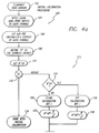
- Fig. 4a is a flow diagram of an illustrative calibration method for the system for matching the outputs of first and second analog-to-digital converters implemented in accordance with the teachings of the present invention.
- the calibration method 100 includes the steps of eliminating zero errors 102.
- step 104 equal nonzero inputs are applied to two of the three windings (channels) by the controller 30.
- the uncorrected outputs of the two channels are denoted as A and B.
- A is arbitrarily defined as the correct value.
- a parameter B' is set equal to B.
- the range of index i is set by a tradeoff between accuracy and speed.
- the routine 113 includes a decision step 114 which compares the value of B' to A. If B' is less than A, then at step 116, a calibration bit i is set. Then, at step 118, B' is incremented by B/2 i and the routine returns to step 114.
- step 114 If at step 114, B' is not less than A, then at step 120, the calibration bit is cleared and B' is decremented by B/2 i and the routine returns to step 114.
- step 124 the calibration of the system 10 is complete and the system goes to normal operational mode 200 depicted in Fig. 4b.
- Fig. 4b is a flow diagram of a normal method of operation for the system 10 of the present invention.
- a and B are denoted the uncalibrated outputs of each channel.
- a parameter A' is set equal to A and B' is set equal to B, respectively.
- the calibration bit is checked to determine if it has been set. If so, at step 212, B' is incremented by B/2 i and the routine returns to step 210. If the calibration bit is not set, at step 214, B' is decremented by B/2 i and the routine returns to step 218.
- A' and B' are the calibrated outputs.
Landscapes
- Engineering & Computer Science (AREA)
- Theoretical Computer Science (AREA)
- Analogue/Digital Conversion (AREA)
- Control Of Electric Motors In General (AREA)
Applications Claiming Priority (2)
| Application Number | Priority Date | Filing Date | Title |
|---|---|---|---|
| US387005 | 1982-06-10 | ||
| US38700599A | 1999-08-31 | 1999-08-31 |
Publications (1)
| Publication Number | Publication Date |
|---|---|
| EP1081861A2 true EP1081861A2 (fr) | 2001-03-07 |
Family
ID=23528035
Family Applications (1)
| Application Number | Title | Priority Date | Filing Date |
|---|---|---|---|
| EP20000116959 Withdrawn EP1081861A2 (fr) | 1999-08-31 | 2000-08-07 | Système de calibration de gain et procédé de création de convertisseurs A/N appariés |
Country Status (2)
| Country | Link |
|---|---|
| EP (1) | EP1081861A2 (fr) |
| JP (1) | JP2001102924A (fr) |
Cited By (2)
| Publication number | Priority date | Publication date | Assignee | Title |
|---|---|---|---|---|
| EP1280277A3 (fr) * | 2001-07-12 | 2004-02-18 | Cirrus Logic, Inc. | Calibration des convertisseurs analogique-numérique isolés |
| CN113721178A (zh) * | 2020-07-01 | 2021-11-30 | 镇江英创电力电子有限公司 | 一种高压隔离变送器全自动校准方法及系统 |
-
2000
- 2000-08-07 EP EP20000116959 patent/EP1081861A2/fr not_active Withdrawn
- 2000-08-23 JP JP2000253091A patent/JP2001102924A/ja active Pending
Cited By (2)
| Publication number | Priority date | Publication date | Assignee | Title |
|---|---|---|---|---|
| EP1280277A3 (fr) * | 2001-07-12 | 2004-02-18 | Cirrus Logic, Inc. | Calibration des convertisseurs analogique-numérique isolés |
| CN113721178A (zh) * | 2020-07-01 | 2021-11-30 | 镇江英创电力电子有限公司 | 一种高压隔离变送器全自动校准方法及系统 |
Also Published As
| Publication number | Publication date |
|---|---|
| JP2001102924A (ja) | 2001-04-13 |
Similar Documents
| Publication | Publication Date | Title |
|---|---|---|
| US5012169A (en) | Motor drive system | |
| US4891764A (en) | Program controlled force measurement and control system | |
| US7483279B2 (en) | Apparatus and method for detecting phase currents of inverter | |
| US11984808B2 (en) | Self-tuning regulator for interleaved power factor correction circuits and method of self-tuning regulation | |
| JP2727315B2 (ja) | 射出成形機の保圧制御方法 | |
| US20090040797A1 (en) | Pulse Width Modulation Method for a Power Converter | |
| JPH0744813B2 (ja) | 位置検出器 | |
| US5619114A (en) | Signal averager for use with motor controller | |
| US6639810B2 (en) | Inverter apparatus for controlling a generator output to sign-wave voltage | |
| EP0104909B1 (fr) | Méthode pour la commande d'un servomoteur et appareil y relatif | |
| US5021724A (en) | Controlling apparatus for induction motor | |
| EP0427527A2 (fr) | Circuit de correction de décalage pour onduleur à modulation de largeur d'impulsion | |
| EP1081861A2 (fr) | Système de calibration de gain et procédé de création de convertisseurs A/N appariés | |
| US10608526B2 (en) | Device and method for calculating switching time | |
| JPH07170799A (ja) | 交流電動機の制御方法と装置および電動機電流の補正方法 | |
| US5208524A (en) | Current control apparatus for PWM control | |
| US20220260615A1 (en) | Apparatus and method for measuring a current flowing through a pwm-controlled inductive load | |
| CN111669181A (zh) | 半导体装置、电机驱动控制装置及电机组件 | |
| US11063546B2 (en) | Motor control device | |
| KR101288196B1 (ko) | 초기 보정 기능을 갖는 모터 구동 장치 및 방법 | |
| KR940006963B1 (ko) | 동기형교류 서보모터의 위상보상방법 | |
| JP3354633B2 (ja) | ステッピングモータ駆動装置 | |
| US9529026B2 (en) | Angle detector, motor drive controller, and motor device | |
| JP2866361B2 (ja) | 射出機構の駆動装置 | |
| JP2003037989A (ja) | Pmモータの自動位相調整装置 |
Legal Events
| Date | Code | Title | Description |
|---|---|---|---|
| PUAI | Public reference made under article 153(3) epc to a published international application that has entered the european phase |
Free format text: ORIGINAL CODE: 0009012 |
|
| AK | Designated contracting states |
Kind code of ref document: A2 Designated state(s): AT BE CH CY DE DK ES FI FR GB GR IE IT LI LU MC NL PT SE |
|
| AX | Request for extension of the european patent |
Free format text: AL;LT;LV;MK;RO;SI |
|
| RAP1 | Party data changed (applicant data changed or rights of an application transferred) |
Owner name: AGILENT TECHNOLOGIES INC. |
|
| RAP1 | Party data changed (applicant data changed or rights of an application transferred) |
Owner name: AGILENT TECHNOLOGIES INC. A DELAWARE CORPORATION |
|
| RAP1 | Party data changed (applicant data changed or rights of an application transferred) |
Owner name: AGILENT TECHNOLOGIES, INC. (A DELAWARE CORPORATION |
|
| STAA | Information on the status of an ep patent application or granted ep patent |
Free format text: STATUS: THE APPLICATION HAS BEEN WITHDRAWN |
|
| 18W | Application withdrawn |
Withdrawal date: 20020829 |