EP1081864B1 - Verfahren zur binär-thermometrischen Umkodierung - Google Patents
Verfahren zur binär-thermometrischen Umkodierung Download PDFInfo
- Publication number
- EP1081864B1 EP1081864B1 EP00203010A EP00203010A EP1081864B1 EP 1081864 B1 EP1081864 B1 EP 1081864B1 EP 00203010 A EP00203010 A EP 00203010A EP 00203010 A EP00203010 A EP 00203010A EP 1081864 B1 EP1081864 B1 EP 1081864B1
- Authority
- EP
- European Patent Office
- Prior art keywords
- signal
- thermometric
- digital
- analog
- vin
- Prior art date
- Legal status (The legal status is an assumption and is not a legal conclusion. Google has not performed a legal analysis and makes no representation as to the accuracy of the status listed.)
- Expired - Lifetime
Links
- 238000000034 method Methods 0.000 title claims description 17
- 238000006243 chemical reaction Methods 0.000 claims description 22
- 230000010287 polarization Effects 0.000 claims description 4
- 235000021183 entrée Nutrition 0.000 description 19
- 230000007704 transition Effects 0.000 description 11
- 230000003071 parasitic effect Effects 0.000 description 9
- 101100328957 Caenorhabditis elegans clk-1 gene Proteins 0.000 description 5
- 101100113692 Caenorhabditis elegans clk-2 gene Proteins 0.000 description 3
- 230000001934 delay Effects 0.000 description 3
- 238000010586 diagram Methods 0.000 description 3
- 238000005265 energy consumption Methods 0.000 description 3
- 230000036039 immunity Effects 0.000 description 3
- 240000008042 Zea mays Species 0.000 description 2
- 230000000295 complement effect Effects 0.000 description 2
- WNTGYJSOUMFZEP-UHFFFAOYSA-N 2-(4-chloro-2-methylphenoxy)propanoic acid Chemical compound OC(=O)C(C)OC1=CC=C(Cl)C=C1C WNTGYJSOUMFZEP-UHFFFAOYSA-N 0.000 description 1
- 238000006677 Appel reaction Methods 0.000 description 1
- XUIMIQQOPSSXEZ-UHFFFAOYSA-N Silicon Chemical compound [Si] XUIMIQQOPSSXEZ-UHFFFAOYSA-N 0.000 description 1
- 241001080024 Telles Species 0.000 description 1
- 229940082150 encore Drugs 0.000 description 1
- 244000045947 parasite Species 0.000 description 1
- 229910052710 silicon Inorganic materials 0.000 description 1
- 239000010703 silicon Substances 0.000 description 1
Images

Classifications
-
- H—ELECTRICITY
- H03—ELECTRONIC CIRCUITRY
- H03M—CODING; DECODING; CODE CONVERSION IN GENERAL
- H03M7/00—Conversion of a code where information is represented by a given sequence or number of digits to a code where the same, similar or subset of information is represented by a different sequence or number of digits
- H03M7/02—Conversion to or from weighted codes, i.e. the weight given to a digit depending on the position of the digit within the block or code word
- H03M7/04—Conversion to or from weighted codes, i.e. the weight given to a digit depending on the position of the digit within the block or code word the radix thereof being two
-
- H—ELECTRICITY
- H03—ELECTRONIC CIRCUITRY
- H03M—CODING; DECODING; CODE CONVERSION IN GENERAL
- H03M7/00—Conversion of a code where information is represented by a given sequence or number of digits to a code where the same, similar or subset of information is represented by a different sequence or number of digits
- H03M7/14—Conversion to or from non-weighted codes
- H03M7/16—Conversion to or from unit-distance codes, e.g. Gray code, reflected binary code
- H03M7/165—Conversion to or from thermometric code
Definitions
- the present invention relates to a method for converting a binary word into a thermometric signal.
- thermometric being governed by an equation of its own, logical door chains are not identical to each other and have different transit times from a chain to the other, which means that not all bits of the thermometric signal will take simultaneously the value that should be theirs, thus causing parasitic transitions in the value of the thermometric signal, and therefore also in the output signal value of the digital to analog converter. This type of conversion error is obviously avoided.
- the present invention aims to remedy to a large extent these disadvantages by proposing a binary / thermometric conversion process that does not require no logic gate network for its implementation.
- the bits of the output signal are all generated from the same way and therefore do not show any significant switching delays, compared to others.
- the conversion and comparison steps can be performed by simple structures, which are therefore inexpensive and do not induce delays in decoding important.
- a process as described above is characterized in that it further comprises inserted between the conversion and comparison, a step of storing the analog signal.
- the memorization of the analog signal allows, to a large extent, to immunize the binary / thermometric conversion process against parasitic transitions of the word input binary, which occur when all bits of said binary word do not take simultaneously the value that should be theirs.
- all the bits of the output signal are generated simultaneously by the comparators, which prevents parasitic transitions from occur in said output signal.
- the converter Digital / Analog has a simple and inexpensive structure. This is made possible thanks to comparators memorize their own output signals, which is equivalent to storage of the thermometric output signal. Indeed, the converter digital / analog described above is vulnerable to parasitic transitions of the binary word input. The storage of the thermometric output signal makes it possible to immunize said signal against parasitic transitions of the analog signal.
- thermometric signal to parasitic transitions of the analogue signal
- a variant of this implementation method makes it possible to halve the complexity of the means of which equipped with the comparators to memorize their output signals.
- the encoder comprises means for storing the signal analog.
- the encoder described above also comprises a first scale of resistances arranged between the first and second power terminals and intended to be biased to the means of a so-called polarization current source, a connection between two resistors adjacent ones being intended to generate an electric potential constituting one of the values of reference to which the analog signal is to be compared.
- the resistive element induced in the digital / analogue converter is constituted by a second scale of resistances, identical, with a resistance close to the first scale of resistance, the maximum value of the current likely to traverse the second scale of resistances being equal to the value of the current discharged by the source of bias current.
- Each comparator is provided with means for storing its own output signal. These means are clocked by a first clock signal Clk1.
- the storage of the thermometric output signal T1 ... TN makes it possible to immunize T1 ... TN said signal against parasitic transitions of the analog signal Vin, which can occur when all the bits of the input binary word IN (0: P-1) do not simultaneously take the value that should be theirs, thus causing non-simultaneous switching of current sources I0 ... IP-1.
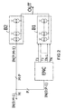
- the encoder ENC indeed comprises MEM means for storing the analog signal. These means comprise a sampler / blocker consisting of a switch SW and a capacitive element C, and driven by a second clock signal Clk2.
- thermometric output signal T1 When this signal is at a logic level 1, the switch SW is closed and the capacitive element C has at its terminals a voltage, which constitutes the analog signal Vin, which reproduces the voltage delivered by the output terminal of the digital converter / analog.
- the second clock signal Clk2 After a predetermined time sufficient for all the bits of the input binary word to have taken the value which must be theirs, the second clock signal Clk2 is at logic level 0 and the value of the analog signal Vin is stored. by the capacitive element C.
- the first and second clock signals Clk1 and Clk2 will advantageously be complementary to one another and have a frequency equal to twice that of the variations of the input binary word IN (0: P-1).
Landscapes
- Engineering & Computer Science (AREA)
- Theoretical Computer Science (AREA)
- Analogue/Digital Conversion (AREA)
Claims (8)
- Verfahren zum Umwandeln eines binären Worts (IN(0:P-1)) in ein thermometrisches Signal (T(1:N), wobei das besagte Verfahren enthält:einen Schritt zur Umwandlung des binären Worts (IN(0:P-1)) in ein analoges Signal (Vin),einen Schritt zum Vergleichen des besagten analogen Signals (Vin) mit einer Vielzahl von Referenzsignalen (V1... VN), um eine Einheit logischer Signale (T1...TN) zu erzeugen, welche das besagte thermometrische Signal (T(1:N)) definieren.
- Verfahren nach Anspruch 1 mit einem Schritt zum Speichern des besagten analogen Signals (Vin), wobei der besagte Schritt zum Speichern zwischen den Schritt zum Umwandeln und den Schritt zum Vergleichen eingefügt wird.
- Thermometrischer Kodierer für den Erhalt eines binären Eingangsworts (IN(0:P-1) und die Ausgabe an einem digitalen Ausgang eines thermometrischen Signals (T(1:N), wobei der besagte thermometrische Kodierer enthält:einen Digital/Analog-Wandler für die Ausgabe eines das binäre Eingangswort IN(0:P- 1)darstellenden analogen Signals (Vin),eine Vielzahl von Vergleichern, jeweils mit einem dafür bestimmten Ausgang ausgestattet, ein das Ergebnis eines Vergleichs zwischen dem Wert des analogen Signals (Vin) und einem Referenzwert (Vi) darstellendes digitales Signal (T1...TN) auszugeben, wobei die Ausgänge der Vergleicher den digitalen Ausgang des thermometrischen Kodierers bilden.
- Thermometrischer Kodierer nach Anspruch 3, in dem der Digital/Analog-Wandler enthält:wobei jeder Vergleicher mit Mitteln zum Abspeichern seines eigenen Ausgangssignals ausgestattet ist.eine Vielzahl von Stromquellen (I0 ... IP-1), wobei die Leitung jeder der Stromquellen (Ij) von einem der Bits (IN(j) des binären Eingangsworts (IN(0:P-1) gesteuert wird und die Stromquellen zwischen einer ersten Versorgungsklemme (GND) und einer Ausgangsklemme des Digital/Analog-Wandlers für die Ausgabe des analogen Signals (Vin) angeordnet sind;ein resistives Element (LD2), zwischen einer zweiten Versorgungsklemme (VCC) und der Ausgangsklemme des Digital/Analog-Wandlers angeordnet,
- Thermometrischer Kodierer nach Anspruch 3 oder 4 mit Mitteln (MEM) zum Abspeichern des analogen Signals (Vin).
- Thermometrischer Kodierer nach Anspruch 3, 4 oder 5 mit außerdem einer ersten Widerstandsstufe (LD1), zwischen der ersten und zweiten Versorgungsklemme (GND, VCC) angeordnet und dafür bestimmt, mittels einer Polarisations-Stromquelle (IT) polarisiert zu werden, wobei eine Verbindung zwischen zwei angrenzenden Widerständen dazu bestimmt ist, ein elektrisches Potenzial zu erzeugen, welches einen der Referenzwerte (Vj) bildet, mit dem das analoge Signal (Vin) verglichen werden muss.
- Kodierer nach Anspruch 3, 4, 5 oder 6, in dem das im Digital/Analog-Wandler enthaltene resistive Element (LD2) aus einer zweiten Widerstandsstufe gebildet wird, bis auf einen Widerstand mit der ersten Widerstandsstufe (LD1) identisch, wobei der maximale Wert des gegebenenfalls durch die zweite Widerstandsstufe fließenden Stroms gleich dem Wert des von der Polarisations-Stromquelle (IT) abgegebenen Stroms ist.
- Vorrichtung zum Umwandeln eines digitalen Eingangssignals (IN(0:M-1)) in ein analoges Ausgangssignal (OUT), wobei die besagte Vorrichtung enthält:einen ersten Akkumulator der Stromquellen (B1) und einen zweiten Akkumulator der Stromquellen (B2) mit miteinander verbundenen Ausgängen und dafür bestimmt, das besagte analoge Ausgangssignal (OUT) auszugeben,einen thermometrischen Kodierer (ENC) entsprechend Anspruch 3 für die Ausgabe eines Ausgangssignals (T(1:N) zum Steuern der Leitung des ersten Akkumulators der Stromquellen (B1) und für den Erhalt eines binären Eingangsworts, (IN(0:P-1) gebildet von den Bits geringen Stellenwerts (IN(0) ... JIN(P-1) des digitalen Eingangssignals (IN(0:M-1), wobei die Bits großen Stellenwerts (IN(P)...IN(M-1) des besagten Eingangssignals (IN(0:M-1)) dafür bestimmt sind, die Leitung des zweiten Akkumulators der Stromquellen (B2) zu steuern.
Applications Claiming Priority (2)
| Application Number | Priority Date | Filing Date | Title |
|---|---|---|---|
| FR9910955A FR2798020A1 (fr) | 1999-08-31 | 1999-08-31 | Procede d'encodage binaire/thermometrique simplifie a resolution amelioree |
| FR9910955 | 1999-08-31 |
Publications (2)
| Publication Number | Publication Date |
|---|---|
| EP1081864A1 EP1081864A1 (de) | 2001-03-07 |
| EP1081864B1 true EP1081864B1 (de) | 2005-01-26 |
Family
ID=9549453
Family Applications (1)
| Application Number | Title | Priority Date | Filing Date |
|---|---|---|---|
| EP00203010A Expired - Lifetime EP1081864B1 (de) | 1999-08-31 | 2000-08-29 | Verfahren zur binär-thermometrischen Umkodierung |
Country Status (6)
| Country | Link |
|---|---|
| US (1) | US6335697B1 (de) |
| EP (1) | EP1081864B1 (de) |
| JP (1) | JP2001102928A (de) |
| KR (1) | KR100678786B1 (de) |
| DE (1) | DE60017651T2 (de) |
| FR (1) | FR2798020A1 (de) |
Families Citing this family (2)
| Publication number | Priority date | Publication date | Assignee | Title |
|---|---|---|---|---|
| US6992609B1 (en) * | 2004-09-17 | 2006-01-31 | Pulselink, Inc. | Digital to analog converter |
| US7425856B2 (en) * | 2006-06-30 | 2008-09-16 | Agere Systems Inc. | Phase interpolator with output amplitude correction |
Family Cites Families (9)
| Publication number | Priority date | Publication date | Assignee | Title |
|---|---|---|---|---|
| GB233171A (en) * | 1924-06-13 | 1925-05-07 | Lawrence Robert Callum | A direction indicator for day and night use on road vehicles |
| DE1220891B (de) * | 1963-10-11 | 1966-07-14 | Olympia Werke Ag | Codeumsetzer mit UND-Schaltungen |
| KR930001724B1 (ko) * | 1985-03-25 | 1993-03-12 | 가부시기가이샤 히다찌세이사꾸쇼 | 저항체 및 이것을 사용한 전자장치 |
| US5283580A (en) * | 1992-09-28 | 1994-02-01 | Motorola, Inc. | Current/resistor digital-to-analog converter having enhanced integral linearity and method of operation |
| US5345234A (en) * | 1993-08-31 | 1994-09-06 | Advanced Micro Devices Inc. | Method and apparatus for combining a flash analog to digital converter with digital to analog functions |
| US5606318A (en) * | 1994-09-30 | 1997-02-25 | Honeywell Inc. | Apparatus for conversion of scaled binary data |
| JP3247810B2 (ja) * | 1994-10-07 | 2002-01-21 | 三菱電機株式会社 | バーグラフデコーダ |
| CA2134310A1 (en) * | 1994-10-25 | 1996-04-26 | Telemus Inc. | Wideband digital peak detector |
| US5706008A (en) * | 1996-03-01 | 1998-01-06 | Analog Devices, Inc. | High bandwidth parallel analog-to-digital converter |
-
1999
- 1999-08-31 FR FR9910955A patent/FR2798020A1/fr not_active Withdrawn
-
2000
- 2000-08-28 US US09/649,676 patent/US6335697B1/en not_active Expired - Lifetime
- 2000-08-29 EP EP00203010A patent/EP1081864B1/de not_active Expired - Lifetime
- 2000-08-29 DE DE60017651T patent/DE60017651T2/de not_active Expired - Lifetime
- 2000-08-30 KR KR1020000050626A patent/KR100678786B1/ko not_active Expired - Fee Related
- 2000-08-31 JP JP2000264237A patent/JP2001102928A/ja not_active Withdrawn
Also Published As
| Publication number | Publication date |
|---|---|
| DE60017651T2 (de) | 2005-12-22 |
| FR2798020A1 (fr) | 2001-03-02 |
| DE60017651D1 (de) | 2005-03-03 |
| EP1081864A1 (de) | 2001-03-07 |
| KR100678786B1 (ko) | 2007-02-05 |
| KR20010021462A (ko) | 2001-03-15 |
| US6335697B1 (en) | 2002-01-01 |
| JP2001102928A (ja) | 2001-04-13 |
Similar Documents
| Publication | Publication Date | Title |
|---|---|---|
| EP0181664B1 (de) | Synchronisierter Komparator | |
| EP1085659B1 (de) | Digital-Analog-Wandler des Stromtyps | |
| FR2577366A1 (fr) | Reseau resistance | |
| EP2944008B1 (de) | Ladungsausgleich innerhalb einer elektrischen batterie | |
| FR2911737A1 (fr) | Procede pour numeriser une grandeur analogique, dispositif de numerisation mettant en oeuvre ce procede et detecteur de rayonnements electromagnetiques integrant un tel dispositif | |
| EP0421896B1 (de) | Analog-Digitalwandler von hoher Umwandlungsfrequenz | |
| FR2699025A1 (fr) | Convertisseur analogique numérique. | |
| FR2755806A1 (fr) | Convertisseur numerique-analogique a sources de courant a autocalibration | |
| FR2961979A1 (fr) | Convertisseur analogique-numerique differentiel a approximations successives | |
| FR2586516A1 (fr) | Convertisseur analogique-numerique a conversion fractionnee comportant un circuit d'isolation entre un noeud de soustraction et un codeur de bits de faible poids | |
| FR2606564A1 (fr) | Dispositif et procede pour engendrer des tensions de reference | |
| FR2527400A1 (fr) | Convertisseur analogique/numerique par impulsion electrique ayant une charge d'entree reduite | |
| FR2700084A1 (fr) | Convertisseur analogique numérique avec échantillonneur bloqueur distribué. | |
| EP0263751B1 (de) | Analog-Digital-Wandler mit geschalteten Kondensatoren | |
| EP1039643A1 (de) | Analog-Digital-Wandleranordnung mit konstanter differentieller nicht-linearität | |
| EP0317421A1 (de) | Analog/Digital-Umwandler vom parallelen Typ | |
| FR2722625A1 (fr) | Convertisseur a/n a comparaison multiple utilisant le principe d'interpolation | |
| FR2767984A1 (fr) | Convertisseur analogique-numerique | |
| EP0817390A1 (de) | Analog-Digital-Wandler | |
| FR2798020A1 (fr) | Procede d'encodage binaire/thermometrique simplifie a resolution amelioree | |
| EP0834990B1 (de) | Programmierbarer digitaler Phasenschieber und Analog-Digital-Umsetzer damit | |
| EP0346988B1 (de) | Integrierte Halbleiterschaltung mit synchronisiertem Komparator | |
| EP0866562A1 (de) | Analog-Digital-Wandler mit einer Verstärkungskalibriervorrichtung | |
| EP0130646B1 (de) | Synchronisierter Komparator | |
| FR2763443A1 (fr) | Circuit de sortie |
Legal Events
| Date | Code | Title | Description |
|---|---|---|---|
| PUAI | Public reference made under article 153(3) epc to a published international application that has entered the european phase |
Free format text: ORIGINAL CODE: 0009012 |
|
| AK | Designated contracting states |
Kind code of ref document: A1 Designated state(s): DE FR GB |
|
| AX | Request for extension of the european patent |
Free format text: AL;LT;LV;MK;RO;SI |
|
| 17P | Request for examination filed |
Effective date: 20010907 |
|
| AKX | Designation fees paid |
Free format text: DE FR GB |
|
| 17Q | First examination report despatched |
Effective date: 20031008 |
|
| GRAP | Despatch of communication of intention to grant a patent |
Free format text: ORIGINAL CODE: EPIDOSNIGR1 |
|
| GRAS | Grant fee paid |
Free format text: ORIGINAL CODE: EPIDOSNIGR3 |
|
| GRAA | (expected) grant |
Free format text: ORIGINAL CODE: 0009210 |
|
| AK | Designated contracting states |
Kind code of ref document: B1 Designated state(s): DE FR GB |
|
| REG | Reference to a national code |
Ref country code: GB Ref legal event code: FG4D Free format text: NOT ENGLISH |
|
| REF | Corresponds to: |
Ref document number: 60017651 Country of ref document: DE Date of ref document: 20050303 Kind code of ref document: P |
|
| GBT | Gb: translation of ep patent filed (gb section 77(6)(a)/1977) |
Effective date: 20050321 |
|
| PLBE | No opposition filed within time limit |
Free format text: ORIGINAL CODE: 0009261 |
|
| STAA | Information on the status of an ep patent application or granted ep patent |
Free format text: STATUS: NO OPPOSITION FILED WITHIN TIME LIMIT |
|
| 26N | No opposition filed |
Effective date: 20051027 |
|
| REG | Reference to a national code |
Ref country code: GB Ref legal event code: 732E |
|
| REG | Reference to a national code |
Ref country code: FR Ref legal event code: TP |
|
| PGFP | Annual fee paid to national office [announced via postgrant information from national office to epo] |
Ref country code: DE Payment date: 20090827 Year of fee payment: 10 |
|
| REG | Reference to a national code |
Ref country code: DE Ref legal event code: R119 Ref document number: 60017651 Country of ref document: DE Effective date: 20110301 |
|
| PG25 | Lapsed in a contracting state [announced via postgrant information from national office to epo] |
Ref country code: DE Free format text: LAPSE BECAUSE OF NON-PAYMENT OF DUE FEES Effective date: 20110301 |
|
| PGFP | Annual fee paid to national office [announced via postgrant information from national office to epo] |
Ref country code: GB Payment date: 20120725 Year of fee payment: 13 |
|
| GBPC | Gb: european patent ceased through non-payment of renewal fee |
Effective date: 20130829 |
|
| PG25 | Lapsed in a contracting state [announced via postgrant information from national office to epo] |
Ref country code: GB Free format text: LAPSE BECAUSE OF NON-PAYMENT OF DUE FEES Effective date: 20130829 |
|
| REG | Reference to a national code |
Ref country code: FR Ref legal event code: PLFP Year of fee payment: 17 |
|
| REG | Reference to a national code |
Ref country code: FR Ref legal event code: PLFP Year of fee payment: 18 |
|
| REG | Reference to a national code |
Ref country code: FR Ref legal event code: PLFP Year of fee payment: 19 |
|
| PGFP | Annual fee paid to national office [announced via postgrant information from national office to epo] |
Ref country code: FR Payment date: 20190722 Year of fee payment: 20 |