EP1083603B1 - Leistungshalbleiter-Modul - Google Patents
Leistungshalbleiter-Modul Download PDFInfo
- Publication number
- EP1083603B1 EP1083603B1 EP00118296A EP00118296A EP1083603B1 EP 1083603 B1 EP1083603 B1 EP 1083603B1 EP 00118296 A EP00118296 A EP 00118296A EP 00118296 A EP00118296 A EP 00118296A EP 1083603 B1 EP1083603 B1 EP 1083603B1
- Authority
- EP
- European Patent Office
- Prior art keywords
- power semiconductor
- semiconductor module
- contact
- module according
- elements
- Prior art date
- Legal status (The legal status is an assumption and is not a legal conclusion. Google has not performed a legal analysis and makes no representation as to the accuracy of the status listed.)
- Expired - Lifetime
Links
Images


Classifications
-
- H—ELECTRICITY
- H10—SEMICONDUCTOR DEVICES; ELECTRIC SOLID-STATE DEVICES NOT OTHERWISE PROVIDED FOR
- H10W—GENERIC PACKAGES, INTERCONNECTIONS, CONNECTORS OR OTHER CONSTRUCTIONAL DETAILS OF DEVICES COVERED BY CLASS H10
- H10W90/00—Package configurations
Definitions
- the invention relates to a power semiconductor module with a Base plate on which at least one equipped with power semiconductor chips Substrate is arranged, which can be pressed against the base plate via pressure elements is.
- the power semiconductors or power semiconductor chips from the basic or Insulate the heat sink, which is used for heat dissipation; find this widely used ceramic insulators in disk form with a metallized surface, e.g. Direct copper bonding (DCB) substrates, application on one of which Surface essentially the power semiconductor chips are arranged while the other surface is thermally coupled to the heat sink.
- DCB Direct copper bonding
- circuit breakers are housed in a common housing, what the assembly technically by reducing the number of components simplified, such as in view of a three-phase bridge circuit for three-phase unidirectional or alternating direction that becomes apparent instead of up to six controllable and six non-controllable circuit breakers in the Execution as individual components from just a single component can exist.
- Examples of power semiconductor modules are widely known, cf. e.g. EP-A-0 265 833, EP 0 277 546B1.
- conductive connectors soldered onto the DCB substrate for example tabs, conductive connectors pressed onto the DCB substrate, in particular Pressure contacts, and in an additional insulator, e.g. a case frame, located conductive connector used to which the electrical connection for example by wire bonding, which is one of these processes previous installation of the insulator.
- thermal coupling to the cooling medium - typically over the underside of the component - forms on a module with a DCB base - see. DE35 21 572A1 - the surface of the DCB ceramic that is not occupied by the chips the bottom of the device.
- the thermal coupling is in the Usually by pressing on a typically metallic heat sink produced by a cooling medium, such as air or cooling liquid, heat is withdrawn, the interface between the DCB bottom and the heat sink advantageously with an intermediate layer made of a thermally bonding Medium, e.g. Thermal grease to be provided.
- the one not used by the chips is used Surface of the DCB ceramic with a usually made of a metal or Composite existing base plate thermally coupled; the coupling can by pressing - cf. DE41 31 200C2, DE41 11 247C2 and DE 41 22 428C2 typically in turn using a thermally bonding Medium, e.g. Thermal paste, by soldering - cf. DE43 38 107C1 - or through other coherent connections, the latter in particular with floor slabs Composites are manufactured.
- the bottom plate in turn is then cooled, which can happen, for example, by pressing on one Heatsink or by flow with a cooling medium, such as air or Coolant, provided a suitable geometric Layout.
- Power semiconductor modules according to State of the art in the described embodiments contradict each other such higher integration insofar as they as closed units with own housing, which are based on requirements such as mechanical stability takes up more volume than with higher integration would be required; this fact is both from the point of view of Cost and space economy as well as in terms of electrical behavior, et al influenced by parasitic lead inductances, disadvantageous; too will the accessibility, for example, to those in the power semiconductor module existing electrical potentials through the housing, which makes it difficult not insignificant design effort to connect the module may require.
- Power semiconductor modules are often characterized by complex Constructions from: So in DE4 131 200C2 a structure with a special designed bridge element.
- a semiconductor unit which has a base plate with a substrate that is equipped with a semiconductor chip.
- the contacting of the semiconductor chip takes place via conductive and flexible power connection elements, which are attached to an outer frame.
- the disadvantage is that the reduction in Dimensions of the module due to the height of the spring-loaded Connection elements are limited.
- the object of the invention is to provide a power semiconductor module to create the type mentioned, its structure depending on the application to the essential Parts is reduced and its integrability into a peripheral device, for example a Control device, is nevertheless promoted.
- a peripheral device for example a Control device
- the greatest possible space economy as well as optimal accessibility of the electrical potentials and thermal Resistance of the connections can be guaranteed.
- what should be created Module can be produced economically by simple manufacturing processes and parts as well by using standard components even more flexibility for offer application-specific customization.
- the pressure elements have elastic and conductive contact cords, which between contact rails and substrates are arranged, the contact cords having an elastic core and have an electrically conductive covering.
- the contact cords are both held down by relatively strong pressure elements against this as well as against that on the opposite side of the contact cords arranged metallizations of the substrates pressed. In this way, one reliable permanent electrical connection between the metallizations of the Substrates with which the semiconductor chips are electrically connected, and the Pressure elements reached via the contact cords; also press the Contact cords the substrates against the one on the opposite side Base plate, so that a favorable heat transfer between the substrates with the to cooling semiconductor chips and the cooled base plate is achieved.
- the arrangement and development of the contact cords according to the invention creates at the same time the prerequisite for an advantageous training of the overall structure of the power semiconductor module according to the invention in the direction of a comparatively simple production, also for different application and Applications. It is characterized by the fact that there are fields on the base plate defining frame can be fixed by means of centering elements, at least some of the fields correspond to substrates using power semiconductor chips are equipped.
- This inventive design of a power semiconductor module gives defined positions for the substrates with the semiconductor chips on them in front. In adaptation to different needs it is possible to all or to cover individual fields with substrates and then to contact them. A change in the tools for making the frame for different applications are therefore not required.
- the contacting of the Chips and the entire production of the power semiconductor module according to the invention improved if on the centering elements and the contact and Counter rails pressure bracket are provided.
- the pressure bracket can be approx Match length and width with the counter rails.
- the frame is grid-shaped and the grid of the Frame integrally formed with it guides for auxiliary contacts. These are thus in one operation together with the frame, in particular manufactured by injection molding.
- the guides are electrical Contacts can be inserted, e.g. connect to one on the Power semiconductor module according to the invention arranged circuit board manufacture, which in turn is an interface to an additional unit, e.g. one Control unit, forms.
- a power semiconductor module 10 according to the invention is described in the following Order of assembly of an exemplary three-phase controlled Bridge circuit explained:
- the base plate 1 is in usually the base plate of a control unit, not shown form, the further, especially electronic assemblies, and in finished design can be closed by additional housing parts.
- the typically metallic base plate 1 can be cooled, e.g. by Air also flows onto cooling fins (not shown) or flows through them Integrated channels with coolant, not specifically shown. If necessary can on the base plate 1 in the area between the threaded bolt 2 Heat transfer to those to be pressed in a later assembly step Medium that improves substrates - e.g. Thermal compound - to be applied.
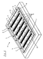
- Fig. 1 also shows a frame placed on the base plate 1 or Housing frame 3. It is, as explained below, in the assembled state of the Power semiconductor module pressed onto the base plate 1. It serves as protection of the power semiconductor chips by the potting compound applied to them prevents it from flowing away, as well as the management of those listed below Components during and partly after assembly. This means that at the Housing frame 3 no special requirements with regard to the recording of forces, so that it is an inexpensive thin-walled plastic part, e.g. made of a thermoset.
- the frame 3 has a circumferential Edge part 4 from a right-angled angle profile; continue a longitudinal web 5 and crossbars 6, which form a grid which defines individual fields 7.
- auxiliary contacts intended at the Longitudinal web 5 are integrally formed guides 8 for auxiliary contacts intended. They have recesses 9 into which these auxiliary contacts be introduced, e.g. for the transmission of control signals to one on the Module to be provided circuit board (not shown).
- the frame 3 has at its on the base plate 1 leg 19, the right angle to the edge part 4 is provided, corresponding to the centering elements 2 Openings so that it can be placed on the base plate 1 and in there the level of the base plate 1 is fixed.
- substrates 13 into the fields 7 of the housing frame 3rd are inserted. These are DCB substrates, as is known, on which the Power semiconductor chips are arranged.
- substrates 13 with different chip configurations - are shown larger chips 11 and smaller chips 12 - without further design changes to use on the structure of the frame 3.
- High efficiency of the manufacturing process is achieved by using identical substrates for all switches.
- the soldered and wire-bonded substrates 13 can during their Manufacturing process can already be checked for errors, so that the installation defective components in the power semiconductor module 10 is to be excluded.
- a plurality of substrates 13 can also be connected in parallel in order to a circuit breaker with a higher number of chips than economical on one Can be realized to build substrate:
- the arrangement shown Three-phase bridge consisting of six switches is with twelve substrates, therefore two of them per switch.
- the substrates 13 correspond in their Dimensions of those of the fields 7, so that during assembly by the Grid of the frame are held reliably.
- counter rails 14 on the Threaded bolt 2 inserted. Their task is also to manage the contact rails 15 to be used for the next assembly step, see FIG. 3 Inclusion of the contact rails 15 and clear fixation are the Counter rails 14 are provided with recesses 16, the cross section of which the Contact rails 15 corresponds to those in the embodiment shown Recesses 16 and the contact rails 15 dimensioned so that they on the Top edge, that is in the area of the exit of the threaded bolts 2 from the Counter rails, flush with the upper edge of the edge part of the frame 3 to lock.
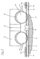
- FIG. 5 is a cross section of a contact rail 15, of contact cords 17th and the substrates 13 contacted therewith.
- the electrical connection on the other hand, the surface pressure of the substrates 13 against the surface heat-dissipating base plate 1 for thermal coupling.
- Advantageous executed contact cords consist of a core 20 made of elastic Material, e.g. Silicone rubber that is conductive and flexible, but not necessarily surrounded by elastic sheath 21, e.g. Copper wire mesh. In this way, one decouples the Features flat pressure - that of which in particular is sufficient heat-resistant elastomer core is applied - and electrical Contacting with the lowest possible resistance and long service life is also carried out in thermal-mechanical cycles.
- the contact cord 17 with its sheath 21 is in the uncompressed state State drawn between the contact rail 15 and the substrate 13 to the compression that occurs during final assembly in the illustration to indicate overlapping areas. In fact, they are in the assembled state Contact cords 17 on the profile 30 of the contact rails 15 and flat on A possible long-term impairment of the chips 11, 12 by Contamination of the encapsulation to be introduced later by the material of the Contact cords 17 can be excluded if an elastomer material, e.g. based on silicone, such as silicone rubber.
- the chips 11, 12 are over a solder layer 22 connected to the substrate 13, which has an electrically conductive copper layer 25
- the layer 24 represents a thermal paste 24, which between Substrate 13 and the base or cooling plate 1 is present.
- contact cords 17 there are preferably two contact cords 17 per contact rail 15. She extend essentially over the length of the contact rails 15, in which further recesses 23 are provided. You can use it to attach one circuit board covering power semiconductor module according to the invention be used.
- the structure mentioned also has an advantageous effect in the construction according to the invention Guide the contact rails 15 in the counter rails 14 from. If push bar 18 are placed on the threaded bolts 2, as shown in Fig. 4, results in by pressing the pressure bracket 18 and counter rails 14 together Stop by means of nuts screwed onto the threaded bolts 2 a constant Contact pressure regardless of the exact torque when tightening, which the Variance of relevant product properties such as electrical and thermal Coupling of the power semiconductors minimized.
- the gate contact springs shown in FIG. 3 and FIG. 4 serve the electrical Connection of control potentials required for controllable switches. she are not burdened with larger currents.
- mechanical Guides 8 are provided in the housing frame, which slide sideways prevent, but otherwise do not absorb mechanical forces.
- a circuit board for example, can be attached in a simple manner to the structure of the power semiconductor module 10 shown in FIG. 4, which is typically done by screwing on using the recesses 23, which can be designed as threaded holes.
- This circuit board can have contact surfaces on its side facing the contact rails, which contact the contact rails on their surface visible in FIG. 4, which contains the recesses 23, by the pressure of the screwing on flat and thus with high current carrying capacity.
- capacitors can be arranged between the positive and negative electrical potential of the intermediate circuit, as are typically used in voltage intermediate circuit converters.
- the construction according to the invention has the particular advantage that the capacitors are located in the immediate vicinity of the semiconductor chips, which, as a low-inductance construction, contributes in particular to optimizing the switching behavior of the semiconductor chips.
- the external connection of the power semiconductor module for example for the external voltage supply and the consumer, typically an electrical machine, can be carried out analogously to the fastening of the printed circuit board using the screw connections already mentioned, which use the recesses 23.
- the control potentials are removed from the substrates 13 by means of contact springs. If a circuit board is attached to the power semiconductor module in the manner described, these contact springs can transmit the control potentials to metallized fields arranged at corresponding locations on the circuit board. This contacting takes place without additional operations during the described mounting of the circuit board.
- the gate drivers will be arranged on the circuit board, which in turn are in the immediate vicinity of the semiconductor chips. This is advantageous both in terms of assembly technology and in terms of electrical behavior.
- the arrangement of the individual components described above results from the connection sequence of the power semiconductor module according to the invention, namely in the case L + , G 1 , L 1 , G 2 , L - , G 4 , L 2 , G 3 shown in FIG. 4 , L + , G 5 , L 3 , G 6 , L - , based on the usual designation scheme for three-phase controlled bridges.
- the pressure bracket 18 can serve as a leading assembly aid when assembling the circuit board.
- a power semiconductor module 10 assembled in this way can already be fully tested, so that components, in particular substrates 13, can still be replaced if necessary. Otherwise, you will continue with partial or complete potting of the power semiconductor module 10 and assembly of the other components of the control unit, the part of which it can form.
- the counter rails 14 and pressure bracket 18 can also be made inexpensive thermosets are manufactured.
Landscapes
- Cooling Or The Like Of Semiconductors Or Solid State Devices (AREA)
- Cooling Or The Like Of Electrical Apparatus (AREA)
- Die Bonding (AREA)
Description
- Fig. 1 bis 4
- die Abfolge des Zusammenbaus wesentlicher Teile eines erfindungsgemäßen Leistungshalbleiter-Moduls in perspektivischer Darstellung und
- Fig. 5
- einen Teilschnitt durch den Gegenstand der Fig. 3 gemäß der Schnittebene V-V.
Claims (9)
- Leistungshalbleiter-Modul (10) mit einer Grundplatte (1), auf der mindestens ein mit Leistungshalbleiter-Chips (11, 12) bestücktes Substrat (13) angeordnet ist, das über Druckelemente an die Grundplatte (1) andrückbar ist, wobei die Druckelemente elastische und leitfähige Anschlußelemente (17) aufweisen, welche zwischen Kontaktschienen (15) und den Substraten (13) angeordnet sind,
dadurch gekennzeichnet, dass die Anschlußelemente Kontaktschnüre (17) sind, die einen elastischen Kern (20) und eine elektrisch leitfähige Umhüllung (21) aufweisen. - Leistungshalbleiter-Modul nach Anspruch 1,
dadurch gekennzeichnet, dass die Kontaktschienen (15) an einer die Kontaktschnüre (17) kontaktierenden Fläche mit einem diesen angepaßten Profil versehen sind. - Leistungshalbleitermodul nach mindestens einem der vorhergehenden Ansprüche,
dadurch gekennzeichnet, dass auf der Grundplatte (1) ein Felder (7) definierender Rahmen (3) mittels Zentrierelementen (2) fixierbar ist, wobei mindestens ein Teil der Felder (7) korrespondierende Substrate (13), die mit Leistungshalbleiter-Chips (11, 12) bestückt sind, aufnimmt. - Leistungshalbleitermodul nach mindestens einem der vorhergehenden Ansprüche,
dadurch gekennzeichnet, dass an einander gegenüberliegenden Seiten des Rahmens (3) Gegenschienen (14) mit Ausnehmungen (16) für die als Kontaktschienen (15) ausgebildeten Druckelemente vorgesehen sind, und dass die Gegenschienen (14) auf den Zentrierelementen (2) angeordnet sind. - Leistungshalbleitermodul nach mindestens einem der vorhergehenden Ansprüche,
dadurch gekennzeichnet, dass die Zentrierelemente Gewindebolzen (2) sind. - Leistungshalbleitermodul nach mindestens einem der vorhergehenden Ansprüche,
dadurch gekennzeichnet, dass das Gitter des Rahmens (3) einstückig mit ihm ausgebildete Führungen (8) für Hilfskontakte aufweist, wobei die Hilfskontakte elektrische Verbindungen zu mindestens einer auf den Kontaktschienen (15) angebrachten Leiterplatte herstellen. - Leistungshalbleitermodul nach mindestens einem der vorhergehenden Ansprüche,
dadurch gekennzeichnet, dass auf den Gegenschienen (14) Druckbügel (18) vorgesehen sind, die die Kontaktschienen (15) niederhalten und über die Zentrierelemente (2) geführt werden. - Leistungshalbleitermodul nach mindestens einem der vorhergehenden Ansprüche,
dadurch gekennzeichnet, dass der Rahmen (3) gitterförmig ausgebildet und mit hochgezogenen Seiten versehen ist. - Leistungshalbleitermodul nach mindestens einem der vorhergehenden Ansprüche,
dadurch gekennzeichnet, dass die Kontaktschienen (15) Einrichtungen, wie Gewindebohrungen (23), aufweisen zum Anschluß der den Laststrom führenden äußeren elektrischen Verbindungen des Leistungshalbleiter-Moduls sowie zur flächigen Kontaktierung mindestens einer Leiterplatte, die mit Bauelementen des Leistungsteils bestückt ist.
Applications Claiming Priority (2)
| Application Number | Priority Date | Filing Date | Title |
|---|---|---|---|
| DE19942770 | 1999-09-08 | ||
| DE19942770A DE19942770A1 (de) | 1999-09-08 | 1999-09-08 | Leistungshalbleiter-Modul |
Publications (3)
| Publication Number | Publication Date |
|---|---|
| EP1083603A2 EP1083603A2 (de) | 2001-03-14 |
| EP1083603A3 EP1083603A3 (de) | 2001-07-11 |
| EP1083603B1 true EP1083603B1 (de) | 2003-12-03 |
Family
ID=7921144
Family Applications (1)
| Application Number | Title | Priority Date | Filing Date |
|---|---|---|---|
| EP00118296A Expired - Lifetime EP1083603B1 (de) | 1999-09-08 | 2000-09-06 | Leistungshalbleiter-Modul |
Country Status (3)
| Country | Link |
|---|---|
| US (1) | US6507108B1 (de) |
| EP (1) | EP1083603B1 (de) |
| DE (2) | DE19942770A1 (de) |
Cited By (1)
| Publication number | Priority date | Publication date | Assignee | Title |
|---|---|---|---|---|
| DE102005047547A1 (de) * | 2005-09-30 | 2007-04-19 | Siemens Ag | Andrückkonzept für Leistungsmodule bestehned aus mindestens einem "Direct Copper Bonding" (DCB) mit Leistungshalbleitern bestückt |
Families Citing this family (16)
| Publication number | Priority date | Publication date | Assignee | Title |
|---|---|---|---|---|
| DE10125695A1 (de) * | 2001-05-25 | 2002-12-05 | Eupec Gmbh & Co Kg | Leistungshalbleiteranordnung |
| DE10141114C1 (de) * | 2001-06-08 | 2002-11-21 | Semikron Elektronik Gmbh | Schaltungsanordnung |
| DE10149886A1 (de) | 2001-10-10 | 2003-04-30 | Eupec Gmbh & Co Kg | Leistunghalbleitermodul |
| DE10159119B4 (de) * | 2001-12-01 | 2005-02-17 | Semikron Elektronik Gmbh | Umrichter in Druckkontaktierung |
| KR100902766B1 (ko) * | 2002-09-27 | 2009-06-15 | 페어차일드코리아반도체 주식회사 | 절연성 세라믹 히트 싱크를 갖는 디스크리트 패키지 |
| DE10316356B4 (de) * | 2003-04-10 | 2012-07-26 | Semikron Elektronik Gmbh & Co. Kg | Modular aufgebautes Leistungshalbleitermodul |
| US7505294B2 (en) * | 2003-05-16 | 2009-03-17 | Continental Automotive Systems Us, Inc. | Tri-level inverter |
| DE10326176A1 (de) * | 2003-06-10 | 2005-01-05 | eupec Europäische Gesellschaft für Leistungshalbleiter mbH | Leistungshalbleitermodul |
| DE102006032441A1 (de) * | 2006-07-13 | 2008-01-17 | Siemens Ag | Vorrichtung aufweisend eine Leiterplatte und ein Modul sowie Verfahren zum Aufbau einer derartigen Vorrichtung |
| DE102006052620B4 (de) * | 2006-11-08 | 2009-07-09 | Semikron Elektronik Gmbh & Co. Kg | Schaltungsanordnung mit einem Leistungsmodul, das mit einer Leiterplatte kombiniert ist. |
| DE102009002993B4 (de) * | 2009-05-11 | 2012-10-04 | Infineon Technologies Ag | Leistungshalbleitermodul mit beabstandeten Schaltungsträgern |
| FR2967796A1 (fr) * | 2010-11-18 | 2012-05-25 | St Microelectronics Sa | Procede et systeme de gestion de l'alimentation d'un composant, par exemple un processeur et d'une memoire, par exemple une memoire cache dudit processeur |
| KR101983160B1 (ko) * | 2013-11-29 | 2019-05-28 | 삼성전기주식회사 | 전력반도체 모듈 |
| DE102014104718B3 (de) * | 2014-04-03 | 2015-08-20 | Infineon Technologies Ag | Halbleiterbaugruppe mit Chiparrays |
| FR3074012B1 (fr) | 2017-11-22 | 2019-12-06 | Safran | Module electronique de puissance |
| CN111405833B (zh) * | 2020-04-15 | 2024-10-01 | 稳力(广东)科技有限公司 | 电机控制器用高性能散热器 |
Family Cites Families (17)
| Publication number | Priority date | Publication date | Assignee | Title |
|---|---|---|---|---|
| DE283236C (de) | ||||
| DE3508456C2 (de) * | 1985-03-09 | 1987-01-08 | Brown, Boveri & Cie Ag, 6800 Mannheim | Leistungshalbleitermodul und Verfahren zur Herstellung eines solchen Moduls |
| DE3521572A1 (de) | 1985-06-15 | 1986-12-18 | Brown, Boveri & Cie Ag, 6800 Mannheim | Leistungshalbleitermodul mit keramiksubstrat |
| JPH088269B2 (ja) | 1986-10-22 | 1996-01-29 | シーメンス、アクチエンゲゼルシヤフト | 半導体デバイス |
| US5060048A (en) | 1986-10-22 | 1991-10-22 | Siemens Aktiengesellschaft & Semikron GmbH | Semiconductor component having at least one power mosfet |
| DE3643288A1 (de) * | 1986-12-18 | 1988-06-30 | Semikron Elektronik Gmbh | Halbleiterbaueinheit |
| US4907068A (en) | 1987-01-21 | 1990-03-06 | Siemens Aktiengesellschaft | Semiconductor arrangement having at least one semiconductor body |
| JP2585834B2 (ja) * | 1990-04-11 | 1997-02-26 | オークマ株式会社 | インバータモジュール |
| DE4111247C3 (de) | 1991-04-08 | 1996-11-21 | Export Contor Ausenhandelsgese | Schaltungsanordnung |
| DE4131200C2 (de) | 1991-09-19 | 1995-05-11 | Export Contor Ausenhandelsgese | Schaltungsanordnung |
| DE4338107C1 (de) | 1993-11-08 | 1995-03-09 | Eupec Gmbh & Co Kg | Halbleiter-Modul |
| JP3269745B2 (ja) * | 1995-01-17 | 2002-04-02 | 株式会社日立製作所 | モジュール型半導体装置 |
| DE19529237C1 (de) * | 1995-08-09 | 1996-08-29 | Semikron Elektronik Gmbh | Schaltungsanordnung |
| JP3396566B2 (ja) * | 1995-10-25 | 2003-04-14 | 三菱電機株式会社 | 半導体装置 |
| DE19630173C2 (de) * | 1996-07-26 | 2001-02-08 | Semikron Elektronik Gmbh | Leistungsmodul mit Halbleiterbauelementen |
| DE19726534A1 (de) * | 1997-06-23 | 1998-12-24 | Asea Brown Boveri | Leistungshalbleitermodul mit geschlossenen Submodulen |
| DE19732738A1 (de) * | 1997-07-30 | 1999-02-04 | Asea Brown Boveri | Leistungshalbleiterbauelemente mit druckausgleichender Kontaktplatte |
-
1999
- 1999-09-08 DE DE19942770A patent/DE19942770A1/de not_active Withdrawn
-
2000
- 2000-09-06 DE DE50004627T patent/DE50004627D1/de not_active Expired - Lifetime
- 2000-09-06 EP EP00118296A patent/EP1083603B1/de not_active Expired - Lifetime
- 2000-09-07 US US09/656,780 patent/US6507108B1/en not_active Expired - Fee Related
Cited By (2)
| Publication number | Priority date | Publication date | Assignee | Title |
|---|---|---|---|---|
| DE102005047547A1 (de) * | 2005-09-30 | 2007-04-19 | Siemens Ag | Andrückkonzept für Leistungsmodule bestehned aus mindestens einem "Direct Copper Bonding" (DCB) mit Leistungshalbleitern bestückt |
| DE102005047547B4 (de) * | 2005-09-30 | 2008-02-14 | Siemens Ag | Andrückkonzept für ein Substrat eines Leistungsmoduls und Leistungsmodul |
Also Published As
| Publication number | Publication date |
|---|---|
| DE50004627D1 (de) | 2004-01-15 |
| DE19942770A1 (de) | 2001-03-15 |
| EP1083603A3 (de) | 2001-07-11 |
| US6507108B1 (en) | 2003-01-14 |
| EP1083603A2 (de) | 2001-03-14 |
Similar Documents
| Publication | Publication Date | Title |
|---|---|---|
| EP1083603B1 (de) | Leistungshalbleiter-Modul | |
| DE10310809B4 (de) | Leistungshalbleitereinrichtung | |
| DE112007002446B4 (de) | Elektronische Schaltungsvorrichtung und Verfahren zu ihrer Herstellung | |
| DE102007013186B4 (de) | Halbleitermodul mit Halbleiterchips und Verfahren zur Herstellung desselben | |
| DE10322745B4 (de) | Leistungshalbleiter-Bauelement mit hoher Abstrahlungseffizienz | |
| DE19854180B4 (de) | Modulgehäuse für Halbleiterbauteile | |
| DE102012206596B4 (de) | Halbleitervorrichtung | |
| DE19939933B4 (de) | Elektronische Leistungs-Moduleinheit | |
| DE102011076235B4 (de) | Leistungshalbleitervorrichtung | |
| DE10238037B4 (de) | Halbleitereinrichtung mit Gehäuse und Halterung | |
| EP1083599B1 (de) | Leistungshalbleitermodul | |
| EP2114113B1 (de) | Leiterplatteneinheit und Verfahren zu deren Herstellung | |
| DE102009055882A1 (de) | Leistungshalbleitervorrichtung | |
| EP2114116B1 (de) | Hybridkühlung | |
| DE10337640A1 (de) | Leistungshalbleitermodul mit verbessertem thermischen Kontakt | |
| EP1642334B1 (de) | Elektronisches leistungsmodul mit gummidichtung und entsprechendes herstellungsverfahren | |
| DE10340297A1 (de) | Schaltungsanordnung für aktive und passive elektrische und elektronische Bauelemente | |
| DE102020124822A1 (de) | Elektrisches Wechselrichter-System | |
| DE102022119251B4 (de) | Halbleitermodul, leistungselektroniksystem und verfahren zur herstellung eines halbleitermoduls und eines leistungselektroniksystems | |
| DE102020109500A1 (de) | Verfahren zum Verbinden von wenigstens zwei elektronischen Bauteilen | |
| DE10249205B3 (de) | Leistungsbauelementanordnung zur mechatronischen Integration von Leistungsbauelementen | |
| DE102022103471A1 (de) | Elektrische Schaltungseinrichtung, elektrische Antriebseinrichtung und Kraftfahrzeug | |
| DE19902462A1 (de) | Halbleiterbauelement mit Chip-on-Chip-Aufbau | |
| DE10139287A1 (de) | Halbleitermodul | |
| DE19904279B4 (de) | Halbleitervorrichtung |
Legal Events
| Date | Code | Title | Description |
|---|---|---|---|
| PUAI | Public reference made under article 153(3) epc to a published international application that has entered the european phase |
Free format text: ORIGINAL CODE: 0009012 |
|
| AK | Designated contracting states |
Kind code of ref document: A2 Designated state(s): DE FR GB IT |
|
| AX | Request for extension of the european patent |
Free format text: AL;LT;LV;MK;RO;SI |
|
| PUAL | Search report despatched |
Free format text: ORIGINAL CODE: 0009013 |
|
| AK | Designated contracting states |
Kind code of ref document: A3 Designated state(s): AT BE CH CY DE DK ES FI FR GB GR IE IT LI LU MC NL PT SE |
|
| AX | Request for extension of the european patent |
Free format text: AL;LT;LV;MK;RO;SI |
|
| RIC1 | Information provided on ipc code assigned before grant |
Free format text: 7H 01L 25/065 A, 7H 01L 23/485 B, 7H 01L 25/07 B |
|
| 17P | Request for examination filed |
Effective date: 20010914 |
|
| AKX | Designation fees paid |
Free format text: DE FR GB IT |
|
| 17Q | First examination report despatched |
Effective date: 20021015 |
|
| GRAH | Despatch of communication of intention to grant a patent |
Free format text: ORIGINAL CODE: EPIDOS IGRA |
|
| GRAS | Grant fee paid |
Free format text: ORIGINAL CODE: EPIDOSNIGR3 |
|
| GRAA | (expected) grant |
Free format text: ORIGINAL CODE: 0009210 |
|
| AK | Designated contracting states |
Kind code of ref document: B1 Designated state(s): DE FR GB IT |
|
| REG | Reference to a national code |
Ref country code: GB Ref legal event code: FG4D Free format text: NOT ENGLISH |
|
| REF | Corresponds to: |
Ref document number: 50004627 Country of ref document: DE Date of ref document: 20040115 Kind code of ref document: P |
|
| GBT | Gb: translation of ep patent filed (gb section 77(6)(a)/1977) |
Effective date: 20040223 |
|
| ET | Fr: translation filed | ||
| PLBE | No opposition filed within time limit |
Free format text: ORIGINAL CODE: 0009261 |
|
| STAA | Information on the status of an ep patent application or granted ep patent |
Free format text: STATUS: NO OPPOSITION FILED WITHIN TIME LIMIT |
|
| 26N | No opposition filed |
Effective date: 20040906 |
|
| PG25 | Lapsed in a contracting state [announced via postgrant information from national office to epo] |
Ref country code: IT Free format text: LAPSE BECAUSE OF NON-PAYMENT OF DUE FEES Effective date: 20050906 |
|
| PGFP | Annual fee paid to national office [announced via postgrant information from national office to epo] |
Ref country code: FR Payment date: 20101005 Year of fee payment: 11 |
|
| PGFP | Annual fee paid to national office [announced via postgrant information from national office to epo] |
Ref country code: GB Payment date: 20100929 Year of fee payment: 11 |
|
| PGFP | Annual fee paid to national office [announced via postgrant information from national office to epo] |
Ref country code: DE Payment date: 20101025 Year of fee payment: 11 |
|
| GBPC | Gb: european patent ceased through non-payment of renewal fee |
Effective date: 20110906 |
|
| REG | Reference to a national code |
Ref country code: FR Ref legal event code: ST Effective date: 20120531 |
|
| REG | Reference to a national code |
Ref country code: DE Ref legal event code: R119 Ref document number: 50004627 Country of ref document: DE Effective date: 20120403 |
|
| PG25 | Lapsed in a contracting state [announced via postgrant information from national office to epo] |
Ref country code: DE Free format text: LAPSE BECAUSE OF NON-PAYMENT OF DUE FEES Effective date: 20120403 |
|
| PG25 | Lapsed in a contracting state [announced via postgrant information from national office to epo] |
Ref country code: GB Free format text: LAPSE BECAUSE OF NON-PAYMENT OF DUE FEES Effective date: 20110906 Ref country code: FR Free format text: LAPSE BECAUSE OF NON-PAYMENT OF DUE FEES Effective date: 20110930 |