EP1083613A2 - Leitende organische Verbindung mit einer pi-Elektronen-Resonanzstruktur - Google Patents
Leitende organische Verbindung mit einer pi-Elektronen-Resonanzstruktur Download PDFInfo
- Publication number
- EP1083613A2 EP1083613A2 EP00307698A EP00307698A EP1083613A2 EP 1083613 A2 EP1083613 A2 EP 1083613A2 EP 00307698 A EP00307698 A EP 00307698A EP 00307698 A EP00307698 A EP 00307698A EP 1083613 A2 EP1083613 A2 EP 1083613A2
- Authority
- EP
- European Patent Office
- Prior art keywords
- liquid crystal
- layer
- phase
- conductive
- conductive liquid
- Prior art date
- Legal status (The legal status is an assumption and is not a legal conclusion. Google has not performed a legal analysis and makes no representation as to the accuracy of the status listed.)
- Withdrawn
Links
- 150000002894 organic compounds Chemical class 0.000 title claims abstract description 34
- 239000004973 liquid crystal related substance Substances 0.000 claims abstract description 159
- 238000001771 vacuum deposition Methods 0.000 claims abstract description 40
- 239000004985 Discotic Liquid Crystal Substance Substances 0.000 claims abstract description 27
- 239000004990 Smectic liquid crystal Substances 0.000 claims abstract description 21
- 239000010410 layer Substances 0.000 claims description 206
- 239000012044 organic layer Substances 0.000 claims description 29
- 238000005401 electroluminescence Methods 0.000 claims description 23
- 239000000758 substrate Substances 0.000 claims description 23
- 238000004020 luminiscence type Methods 0.000 claims description 20
- 238000010438 heat treatment Methods 0.000 claims description 11
- 238000003475 lamination Methods 0.000 claims description 8
- 239000012071 phase Substances 0.000 description 96
- TVIVIEFSHFOWTE-UHFFFAOYSA-K tri(quinolin-8-yloxy)alumane Chemical compound [Al+3].C1=CN=C2C([O-])=CC=CC2=C1.C1=CN=C2C([O-])=CC=CC2=C1.C1=CN=C2C([O-])=CC=CC2=C1 TVIVIEFSHFOWTE-UHFFFAOYSA-K 0.000 description 36
- 238000002347 injection Methods 0.000 description 32
- 239000007924 injection Substances 0.000 description 32
- 239000010408 film Substances 0.000 description 27
- 150000001875 compounds Chemical class 0.000 description 24
- 230000006870 function Effects 0.000 description 18
- 229910052751 metal Inorganic materials 0.000 description 16
- 239000002184 metal Substances 0.000 description 16
- 239000000463 material Substances 0.000 description 15
- 239000013078 crystal Substances 0.000 description 12
- 239000011521 glass Substances 0.000 description 12
- 230000000052 comparative effect Effects 0.000 description 10
- 230000007704 transition Effects 0.000 description 10
- 230000005684 electric field Effects 0.000 description 9
- 229910001148 Al-Li alloy Inorganic materials 0.000 description 8
- XCJYREBRNVKWGJ-UHFFFAOYSA-N copper(II) phthalocyanine Chemical compound [Cu+2].C12=CC=CC=C2C(N=C2[N-]C(C3=CC=CC=C32)=N2)=NC1=NC([C]1C=CC=CC1=1)=NC=1N=C1[C]3C=CC=CC3=C2[N-]1 XCJYREBRNVKWGJ-UHFFFAOYSA-N 0.000 description 7
- IBHBKWKFFTZAHE-UHFFFAOYSA-N n-[4-[4-(n-naphthalen-1-ylanilino)phenyl]phenyl]-n-phenylnaphthalen-1-amine Chemical compound C1=CC=CC=C1N(C=1C2=CC=CC=C2C=CC=1)C1=CC=C(C=2C=CC(=CC=2)N(C=2C=CC=CC=2)C=2C3=CC=CC=C3C=CC=2)C=C1 IBHBKWKFFTZAHE-UHFFFAOYSA-N 0.000 description 7
- 238000004528 spin coating Methods 0.000 description 7
- 230000000694 effects Effects 0.000 description 6
- 230000006872 improvement Effects 0.000 description 6
- 238000000034 method Methods 0.000 description 6
- -1 triphenylene compound Chemical class 0.000 description 6
- 229910017073 AlLi Inorganic materials 0.000 description 5
- 229940125898 compound 5 Drugs 0.000 description 5
- 230000001747 exhibiting effect Effects 0.000 description 5
- 238000004770 highest occupied molecular orbital Methods 0.000 description 5
- 239000011368 organic material Substances 0.000 description 5
- AHLBNYSZXLDEJQ-FWEHEUNISA-N orlistat Chemical compound CCCCCCCCCCC[C@H](OC(=O)[C@H](CC(C)C)NC=O)C[C@@H]1OC(=O)[C@H]1CCCCCC AHLBNYSZXLDEJQ-FWEHEUNISA-N 0.000 description 5
- 125000005580 triphenylene group Chemical group 0.000 description 5
- 230000008901 benefit Effects 0.000 description 4
- 230000015572 biosynthetic process Effects 0.000 description 4
- 230000008859 change Effects 0.000 description 4
- 238000000151 deposition Methods 0.000 description 4
- 230000008021 deposition Effects 0.000 description 4
- 230000008520 organization Effects 0.000 description 4
- 238000004544 sputter deposition Methods 0.000 description 4
- HEDRZPFGACZZDS-UHFFFAOYSA-N Chloroform Chemical compound ClC(Cl)Cl HEDRZPFGACZZDS-UHFFFAOYSA-N 0.000 description 3
- 229910045601 alloy Inorganic materials 0.000 description 3
- 239000000956 alloy Substances 0.000 description 3
- 230000004888 barrier function Effects 0.000 description 3
- 239000012535 impurity Substances 0.000 description 3
- 239000007791 liquid phase Substances 0.000 description 3
- 238000004768 lowest unoccupied molecular orbital Methods 0.000 description 3
- 150000002739 metals Chemical class 0.000 description 3
- 238000001228 spectrum Methods 0.000 description 3
- FYYHWMGAXLPEAU-UHFFFAOYSA-N Magnesium Chemical compound [Mg] FYYHWMGAXLPEAU-UHFFFAOYSA-N 0.000 description 2
- SLGBZMMZGDRARJ-UHFFFAOYSA-N Triphenylene Natural products C1=CC=C2C3=CC=CC=C3C3=CC=CC=C3C2=C1 SLGBZMMZGDRARJ-UHFFFAOYSA-N 0.000 description 2
- XLOMVQKBTHCTTD-UHFFFAOYSA-N Zinc monoxide Chemical compound [Zn]=O XLOMVQKBTHCTTD-UHFFFAOYSA-N 0.000 description 2
- 229910052782 aluminium Inorganic materials 0.000 description 2
- XAGFODPZIPBFFR-UHFFFAOYSA-N aluminium Chemical compound [Al] XAGFODPZIPBFFR-UHFFFAOYSA-N 0.000 description 2
- MWPLVEDNUUSJAV-UHFFFAOYSA-N anthracene Chemical compound C1=CC=CC2=CC3=CC=CC=C3C=C21 MWPLVEDNUUSJAV-UHFFFAOYSA-N 0.000 description 2
- 125000003118 aryl group Chemical group 0.000 description 2
- HFACYLZERDEVSX-UHFFFAOYSA-N benzidine Chemical compound C1=CC(N)=CC=C1C1=CC=C(N)C=C1 HFACYLZERDEVSX-UHFFFAOYSA-N 0.000 description 2
- IOJUPLGTWVMSFF-UHFFFAOYSA-N benzothiazole Chemical group C1=CC=C2SC=NC2=C1 IOJUPLGTWVMSFF-UHFFFAOYSA-N 0.000 description 2
- 230000000903 blocking effect Effects 0.000 description 2
- 238000001816 cooling Methods 0.000 description 2
- 230000006866 deterioration Effects 0.000 description 2
- JNTHRSHGARDABO-UHFFFAOYSA-N dibenzo[a,l]pyrene Chemical group C1=CC=CC2=C3C4=CC=CC=C4C=C(C=C4)C3=C3C4=CC=CC3=C21 JNTHRSHGARDABO-UHFFFAOYSA-N 0.000 description 2
- 238000002474 experimental method Methods 0.000 description 2
- 230000003993 interaction Effects 0.000 description 2
- 239000011777 magnesium Substances 0.000 description 2
- 229910052749 magnesium Inorganic materials 0.000 description 2
- 125000001624 naphthyl group Chemical group 0.000 description 2
- 230000003287 optical effect Effects 0.000 description 2
- 150000004866 oxadiazoles Chemical class 0.000 description 2
- 125000002080 perylenyl group Chemical class C1(=CC=C2C=CC=C3C4=CC=CC5=CC=CC(C1=C23)=C45)* 0.000 description 2
- CSHWQDPOILHKBI-UHFFFAOYSA-N peryrene Natural products C1=CC(C2=CC=CC=3C2=C2C=CC=3)=C3C2=CC=CC3=C1 CSHWQDPOILHKBI-UHFFFAOYSA-N 0.000 description 2
- YNPNZTXNASCQKK-UHFFFAOYSA-N phenanthrene Chemical group C1=CC=C2C3=CC=CC=C3C=CC2=C1 YNPNZTXNASCQKK-UHFFFAOYSA-N 0.000 description 2
- 125000001997 phenyl group Chemical group [H]C1=C([H])C([H])=C(*)C([H])=C1[H] 0.000 description 2
- BASFCYQUMIYNBI-UHFFFAOYSA-N platinum Chemical compound [Pt] BASFCYQUMIYNBI-UHFFFAOYSA-N 0.000 description 2
- 230000008569 process Effects 0.000 description 2
- 230000006798 recombination Effects 0.000 description 2
- 238000005215 recombination Methods 0.000 description 2
- 239000007787 solid Substances 0.000 description 2
- 239000002904 solvent Substances 0.000 description 2
- 238000002366 time-of-flight method Methods 0.000 description 2
- 238000007740 vapor deposition Methods 0.000 description 2
- QLZBVNHNENRPAK-UHFFFAOYSA-N (3,6,7,10,11-pentapentoxytriphenylen-2-yl) cyclohexanecarboxylate Chemical compound CCCCCOC1=CC2=C3C=C(OCCCCC)C(OCCCCC)=CC3=C3C=C(OCCCCC)C(OCCCCC)=CC3=C2C=C1OC(=O)C1CCCCC1 QLZBVNHNENRPAK-UHFFFAOYSA-N 0.000 description 1
- FXQKTVQNFVFWAA-UHFFFAOYSA-N 1,2,3,4,5,6-hexahexoxytriphenylene Chemical group CCCCCCOC1=C(OCCCCCC)C(OCCCCCC)=C2C3=C(OCCCCCC)C(OCCCCCC)=CC=C3C3=CC=CC=C3C2=C1OCCCCCC FXQKTVQNFVFWAA-UHFFFAOYSA-N 0.000 description 1
- BCMCBBGGLRIHSE-UHFFFAOYSA-N 1,3-benzoxazole Chemical class C1=CC=C2OC=NC2=C1 BCMCBBGGLRIHSE-UHFFFAOYSA-N 0.000 description 1
- 125000000355 1,3-benzoxazolyl group Chemical group O1C(=NC2=C1C=CC=C2)* 0.000 description 1
- PNJTZJDRBBJYKP-UHFFFAOYSA-N 1-[2,2-bis(4-methylphenyl)ethenyl]-4-[4-[2,2-bis(4-methylphenyl)ethenyl]phenyl]benzene Chemical group C1=CC(C)=CC=C1C(C=1C=CC(C)=CC=1)=CC1=CC=C(C=2C=CC(C=C(C=3C=CC(C)=CC=3)C=3C=CC(C)=CC=3)=CC=2)C=C1 PNJTZJDRBBJYKP-UHFFFAOYSA-N 0.000 description 1
- IANQTJSKSUMEQM-UHFFFAOYSA-N 1-benzofuran Chemical group C1=CC=C2OC=CC2=C1 IANQTJSKSUMEQM-UHFFFAOYSA-N 0.000 description 1
- IYDMICQAKLQHLA-UHFFFAOYSA-N 1-phenylnaphthalene Chemical class C1=CC=CC=C1C1=CC=CC2=CC=CC=C12 IYDMICQAKLQHLA-UHFFFAOYSA-N 0.000 description 1
- DFTDNOACRIXKPA-UHFFFAOYSA-N 2-butoxy-6-(3-octylphenyl)naphthalene Chemical compound CCCCCCCCC1=CC=CC(C=2C=C3C=CC(OCCCC)=CC3=CC=2)=C1 DFTDNOACRIXKPA-UHFFFAOYSA-N 0.000 description 1
- TXAORCSLBBFWGZ-UHFFFAOYSA-N 2-butoxy-6-octan-4-ylnaphthalene Chemical compound C1=C(C(CCC)CCCC)C=CC2=CC(OCCCC)=CC=C21 TXAORCSLBBFWGZ-UHFFFAOYSA-N 0.000 description 1
- WWVFJJKBBZXWFV-UHFFFAOYSA-N 2-naphthalen-1-yl-5-phenyl-1,3-oxazole Chemical compound C=1N=C(C=2C3=CC=CC=C3C=CC=2)OC=1C1=CC=CC=C1 WWVFJJKBBZXWFV-UHFFFAOYSA-N 0.000 description 1
- XBHOUXSGHYZCNH-UHFFFAOYSA-N 2-phenyl-1,3-benzothiazole Chemical class C1=CC=CC=C1C1=NC2=CC=CC=C2S1 XBHOUXSGHYZCNH-UHFFFAOYSA-N 0.000 description 1
- OGGKVJMNFFSDEV-UHFFFAOYSA-N 3-methyl-n-[4-[4-(n-(3-methylphenyl)anilino)phenyl]phenyl]-n-phenylaniline Chemical compound CC1=CC=CC(N(C=2C=CC=CC=2)C=2C=CC(=CC=2)C=2C=CC(=CC=2)N(C=2C=CC=CC=2)C=2C=C(C)C=CC=2)=C1 OGGKVJMNFFSDEV-UHFFFAOYSA-N 0.000 description 1
- VESMRDNBVZOIEN-UHFFFAOYSA-N 9h-carbazole-1,2-diamine Chemical class C1=CC=C2C3=CC=C(N)C(N)=C3NC2=C1 VESMRDNBVZOIEN-UHFFFAOYSA-N 0.000 description 1
- 229910001316 Ag alloy Inorganic materials 0.000 description 1
- YLYPIBBGWLKELC-RMKNXTFCSA-N CC(OC(/C=C/c(cc1)ccc1N(C)C)=C1)=CC1=C(C#N)C#N Chemical compound CC(OC(/C=C/c(cc1)ccc1N(C)C)=C1)=CC1=C(C#N)C#N YLYPIBBGWLKELC-RMKNXTFCSA-N 0.000 description 1
- 229910000881 Cu alloy Inorganic materials 0.000 description 1
- DGAQECJNVWCQMB-PUAWFVPOSA-M Ilexoside XXIX Chemical compound C[C@@H]1CC[C@@]2(CC[C@@]3(C(=CC[C@H]4[C@]3(CC[C@@H]5[C@@]4(CC[C@@H](C5(C)C)OS(=O)(=O)[O-])C)C)[C@@H]2[C@]1(C)O)C)C(=O)O[C@H]6[C@@H]([C@H]([C@@H]([C@H](O6)CO)O)O)O.[Na+] DGAQECJNVWCQMB-PUAWFVPOSA-M 0.000 description 1
- 229910000846 In alloy Inorganic materials 0.000 description 1
- 229910000799 K alloy Inorganic materials 0.000 description 1
- WHXSMMKQMYFTQS-UHFFFAOYSA-N Lithium Chemical compound [Li] WHXSMMKQMYFTQS-UHFFFAOYSA-N 0.000 description 1
- 229910019015 Mg-Ag Inorganic materials 0.000 description 1
- ZLMJMSJWJFRBEC-UHFFFAOYSA-N Potassium Chemical compound [K] ZLMJMSJWJFRBEC-UHFFFAOYSA-N 0.000 description 1
- JUJWROOIHBZHMG-UHFFFAOYSA-N Pyridine Chemical group C1=CC=NC=C1 JUJWROOIHBZHMG-UHFFFAOYSA-N 0.000 description 1
- NRCMAYZCPIVABH-UHFFFAOYSA-N Quinacridone Chemical class N1C2=CC=CC=C2C(=O)C2=C1C=C1C(=O)C3=CC=CC=C3NC1=C2 NRCMAYZCPIVABH-UHFFFAOYSA-N 0.000 description 1
- 229910000676 Si alloy Inorganic materials 0.000 description 1
- 239000007983 Tris buffer Substances 0.000 description 1
- DGEZNRSVGBDHLK-UHFFFAOYSA-N [1,10]phenanthroline Chemical compound C1=CN=C2C3=NC=CC=C3C=CC2=C1 DGEZNRSVGBDHLK-UHFFFAOYSA-N 0.000 description 1
- JFBZPFYRPYOZCQ-UHFFFAOYSA-N [Li].[Al] Chemical compound [Li].[Al] JFBZPFYRPYOZCQ-UHFFFAOYSA-N 0.000 description 1
- JHYLKGDXMUDNEO-UHFFFAOYSA-N [Mg].[In] Chemical compound [Mg].[In] JHYLKGDXMUDNEO-UHFFFAOYSA-N 0.000 description 1
- 229910052783 alkali metal Inorganic materials 0.000 description 1
- 150000001340 alkali metals Chemical class 0.000 description 1
- 229910052784 alkaline earth metal Inorganic materials 0.000 description 1
- 150000001342 alkaline earth metals Chemical class 0.000 description 1
- 125000003545 alkoxy group Chemical group 0.000 description 1
- WPPDFTBPZNZZRP-UHFFFAOYSA-N aluminum copper Chemical compound [Al].[Cu] WPPDFTBPZNZZRP-UHFFFAOYSA-N 0.000 description 1
- 239000010405 anode material Substances 0.000 description 1
- 125000005577 anthracene group Chemical group 0.000 description 1
- PYKYMHQGRFAEBM-UHFFFAOYSA-N anthraquinone Chemical class CCC(=O)c1c(O)c2C(=O)C3C(C=CC=C3O)C(=O)c2cc1CC(=O)OC PYKYMHQGRFAEBM-UHFFFAOYSA-N 0.000 description 1
- 150000004056 anthraquinones Chemical class 0.000 description 1
- 150000004984 aromatic diamines Chemical class 0.000 description 1
- 125000003828 azulenyl group Chemical group 0.000 description 1
- 125000003785 benzimidazolyl group Chemical group N1=C(NC2=C1C=CC=C2)* 0.000 description 1
- 229910052790 beryllium Inorganic materials 0.000 description 1
- ATBAMAFKBVZNFJ-UHFFFAOYSA-N beryllium atom Chemical compound [Be] ATBAMAFKBVZNFJ-UHFFFAOYSA-N 0.000 description 1
- 239000010406 cathode material Substances 0.000 description 1
- 239000003086 colorant Substances 0.000 description 1
- 229940125904 compound 1 Drugs 0.000 description 1
- 229940125782 compound 2 Drugs 0.000 description 1
- 229940126214 compound 3 Drugs 0.000 description 1
- GBRBMTNGQBKBQE-UHFFFAOYSA-L copper;diiodide Chemical compound I[Cu]I GBRBMTNGQBKBQE-UHFFFAOYSA-L 0.000 description 1
- 125000000332 coumarinyl group Chemical class O1C(=O)C(=CC2=CC=CC=C12)* 0.000 description 1
- 230000006378 damage Effects 0.000 description 1
- 230000007547 defect Effects 0.000 description 1
- 230000001419 dependent effect Effects 0.000 description 1
- 238000001035 drying Methods 0.000 description 1
- 239000007772 electrode material Substances 0.000 description 1
- 238000005516 engineering process Methods 0.000 description 1
- 239000003574 free electron Substances 0.000 description 1
- PCHJSUWPFVWCPO-UHFFFAOYSA-N gold Chemical compound [Au] PCHJSUWPFVWCPO-UHFFFAOYSA-N 0.000 description 1
- 229910052737 gold Inorganic materials 0.000 description 1
- 239000010931 gold Substances 0.000 description 1
- RBTKNAXYKSUFRK-UHFFFAOYSA-N heliogen blue Chemical compound [Cu].[N-]1C2=C(C=CC=C3)C3=C1N=C([N-]1)C3=CC=CC=C3C1=NC([N-]1)=C(C=CC=C3)C3=C1N=C([N-]1)C3=CC=CC=C3C1=N2 RBTKNAXYKSUFRK-UHFFFAOYSA-N 0.000 description 1
- XHJPOZDMDBETDO-UHFFFAOYSA-N hexabenzo[a,d,g,j,m,p]coronene Chemical group C1=CC=CC2=C(C3=C45)C6=CC=CC=C6C4=C(C=CC=C4)C4=C(C=4C6=CC=CC=4)C5=C4C6=C(C=CC=C5)C5=C(C=5C6=CC=CC=5)C4=C3C6=C21 XHJPOZDMDBETDO-UHFFFAOYSA-N 0.000 description 1
- 230000002209 hydrophobic effect Effects 0.000 description 1
- 125000003453 indazolyl group Chemical group N1N=C(C2=C1C=CC=C2)* 0.000 description 1
- 229910003437 indium oxide Inorganic materials 0.000 description 1
- PJXISJQVUVHSOJ-UHFFFAOYSA-N indium(iii) oxide Chemical compound [O-2].[O-2].[O-2].[In+3].[In+3] PJXISJQVUVHSOJ-UHFFFAOYSA-N 0.000 description 1
- AMGQUBHHOARCQH-UHFFFAOYSA-N indium;oxotin Chemical compound [In].[Sn]=O AMGQUBHHOARCQH-UHFFFAOYSA-N 0.000 description 1
- 125000001041 indolyl group Chemical group 0.000 description 1
- 230000009545 invasion Effects 0.000 description 1
- 125000002183 isoquinolinyl group Chemical group C1(=NC=CC2=CC=CC=C12)* 0.000 description 1
- 239000007788 liquid Substances 0.000 description 1
- 229910052744 lithium Inorganic materials 0.000 description 1
- 239000001989 lithium alloy Substances 0.000 description 1
- 230000033001 locomotion Effects 0.000 description 1
- SJCKRGFTWFGHGZ-UHFFFAOYSA-N magnesium silver Chemical compound [Mg].[Ag] SJCKRGFTWFGHGZ-UHFFFAOYSA-N 0.000 description 1
- 238000005259 measurement Methods 0.000 description 1
- 230000007246 mechanism Effects 0.000 description 1
- QSHDDOUJBYECFT-UHFFFAOYSA-N mercury Chemical compound [Hg] QSHDDOUJBYECFT-UHFFFAOYSA-N 0.000 description 1
- 229910052753 mercury Inorganic materials 0.000 description 1
- 239000007769 metal material Substances 0.000 description 1
- 229910044991 metal oxide Inorganic materials 0.000 description 1
- 150000004706 metal oxides Chemical class 0.000 description 1
- 239000000203 mixture Substances 0.000 description 1
- DCZNSJVFOQPSRV-UHFFFAOYSA-N n,n-diphenyl-4-[4-(n-phenylanilino)phenyl]aniline Chemical class C1=CC=CC=C1N(C=1C=CC(=CC=1)C=1C=CC(=CC=1)N(C=1C=CC=CC=1)C=1C=CC=CC=1)C1=CC=CC=C1 DCZNSJVFOQPSRV-UHFFFAOYSA-N 0.000 description 1
- 230000003647 oxidation Effects 0.000 description 1
- 238000007254 oxidation reaction Methods 0.000 description 1
- 238000005424 photoluminescence Methods 0.000 description 1
- IEQIEDJGQAUEQZ-UHFFFAOYSA-N phthalocyanine Chemical group N1C(N=C2C3=CC=CC=C3C(N=C3C4=CC=CC=C4C(=N4)N3)=N2)=C(C=CC=C2)C2=C1N=C1C2=CC=CC=C2C4=N1 IEQIEDJGQAUEQZ-UHFFFAOYSA-N 0.000 description 1
- 238000009832 plasma treatment Methods 0.000 description 1
- 229910052697 platinum Inorganic materials 0.000 description 1
- 229920000642 polymer Polymers 0.000 description 1
- BITYAPCSNKJESK-UHFFFAOYSA-N potassiosodium Chemical compound [Na].[K] BITYAPCSNKJESK-UHFFFAOYSA-N 0.000 description 1
- 229910052700 potassium Inorganic materials 0.000 description 1
- 239000011591 potassium Substances 0.000 description 1
- 230000001737 promoting effect Effects 0.000 description 1
- 230000001681 protective effect Effects 0.000 description 1
- 125000003373 pyrazinyl group Chemical group 0.000 description 1
- PBMFSQRYOILNGV-UHFFFAOYSA-N pyridazine Chemical group C1=CC=NN=C1 PBMFSQRYOILNGV-UHFFFAOYSA-N 0.000 description 1
- 125000000714 pyrimidinyl group Chemical group 0.000 description 1
- 125000002294 quinazolinyl group Chemical group N1=C(N=CC2=CC=CC=C12)* 0.000 description 1
- 125000002943 quinolinyl group Chemical group N1=C(C=CC2=CC=CC=C12)* 0.000 description 1
- 125000001567 quinoxalinyl group Chemical group N1=C(C=NC2=CC=CC=C12)* 0.000 description 1
- 230000009257 reactivity Effects 0.000 description 1
- 239000004065 semiconductor Substances 0.000 description 1
- 229910052708 sodium Inorganic materials 0.000 description 1
- 239000011734 sodium Substances 0.000 description 1
- 239000000243 solution Substances 0.000 description 1
- PJANXHGTPQOBST-UHFFFAOYSA-N stilbene Chemical group C=1C=CC=CC=1C=CC1=CC=CC=C1 PJANXHGTPQOBST-UHFFFAOYSA-N 0.000 description 1
- 125000005504 styryl group Chemical group 0.000 description 1
- 239000013589 supplement Substances 0.000 description 1
- 239000010409 thin film Substances 0.000 description 1
- 125000000101 thioether group Chemical group 0.000 description 1
- 229910052718 tin Inorganic materials 0.000 description 1
- XOLBLPGZBRYERU-UHFFFAOYSA-N tin dioxide Chemical compound O=[Sn]=O XOLBLPGZBRYERU-UHFFFAOYSA-N 0.000 description 1
- 229910001887 tin oxide Inorganic materials 0.000 description 1
- 150000001651 triphenylamine derivatives Chemical class 0.000 description 1
- QVWDCTQRORVHHT-UHFFFAOYSA-N tropone Chemical group O=C1C=CC=CC=C1 QVWDCTQRORVHHT-UHFFFAOYSA-N 0.000 description 1
- YGPLLMPPZRUGTJ-UHFFFAOYSA-N truxene Chemical group C1C2=CC=CC=C2C(C2=C3C4=CC=CC=C4C2)=C1C1=C3CC2=CC=CC=C21 YGPLLMPPZRUGTJ-UHFFFAOYSA-N 0.000 description 1
- 238000007738 vacuum evaporation Methods 0.000 description 1
- 238000009834 vaporization Methods 0.000 description 1
- 230000008016 vaporization Effects 0.000 description 1
- 239000011787 zinc oxide Substances 0.000 description 1
Images

Classifications
-
- H—ELECTRICITY
- H10—SEMICONDUCTOR DEVICES; ELECTRIC SOLID-STATE DEVICES NOT OTHERWISE PROVIDED FOR
- H10K—ORGANIC ELECTRIC SOLID-STATE DEVICES
- H10K50/00—Organic light-emitting devices
- H10K50/10—OLEDs or polymer light-emitting diodes [PLED]
- H10K50/11—OLEDs or polymer light-emitting diodes [PLED] characterised by the electroluminescent [EL] layers
-
- H—ELECTRICITY
- H10—SEMICONDUCTOR DEVICES; ELECTRIC SOLID-STATE DEVICES NOT OTHERWISE PROVIDED FOR
- H10K—ORGANIC ELECTRIC SOLID-STATE DEVICES
- H10K85/00—Organic materials used in the body or electrodes of devices covered by this subclass
- H10K85/60—Organic compounds having low molecular weight
- H10K85/615—Polycyclic condensed aromatic hydrocarbons, e.g. anthracene
- H10K85/622—Polycyclic condensed aromatic hydrocarbons, e.g. anthracene containing four rings, e.g. pyrene
-
- H—ELECTRICITY
- H10—SEMICONDUCTOR DEVICES; ELECTRIC SOLID-STATE DEVICES NOT OTHERWISE PROVIDED FOR
- H10K—ORGANIC ELECTRIC SOLID-STATE DEVICES
- H10K85/00—Organic materials used in the body or electrodes of devices covered by this subclass
- H10K85/731—Liquid crystalline materials
-
- C—CHEMISTRY; METALLURGY
- C09—DYES; PAINTS; POLISHES; NATURAL RESINS; ADHESIVES; COMPOSITIONS NOT OTHERWISE PROVIDED FOR; APPLICATIONS OF MATERIALS NOT OTHERWISE PROVIDED FOR
- C09K—MATERIALS FOR MISCELLANEOUS APPLICATIONS, NOT PROVIDED FOR ELSEWHERE
- C09K2323/00—Functional layers of liquid crystal optical display excluding electroactive liquid crystal layer characterised by chemical composition
-
- C—CHEMISTRY; METALLURGY
- C09—DYES; PAINTS; POLISHES; NATURAL RESINS; ADHESIVES; COMPOSITIONS NOT OTHERWISE PROVIDED FOR; APPLICATIONS OF MATERIALS NOT OTHERWISE PROVIDED FOR
- C09K—MATERIALS FOR MISCELLANEOUS APPLICATIONS, NOT PROVIDED FOR ELSEWHERE
- C09K2323/00—Functional layers of liquid crystal optical display excluding electroactive liquid crystal layer characterised by chemical composition
- C09K2323/04—Charge transferring layer characterised by chemical composition, i.e. conductive
-
- H—ELECTRICITY
- H10—SEMICONDUCTOR DEVICES; ELECTRIC SOLID-STATE DEVICES NOT OTHERWISE PROVIDED FOR
- H10K—ORGANIC ELECTRIC SOLID-STATE DEVICES
- H10K85/00—Organic materials used in the body or electrodes of devices covered by this subclass
- H10K85/30—Coordination compounds
- H10K85/311—Phthalocyanine
-
- H—ELECTRICITY
- H10—SEMICONDUCTOR DEVICES; ELECTRIC SOLID-STATE DEVICES NOT OTHERWISE PROVIDED FOR
- H10K—ORGANIC ELECTRIC SOLID-STATE DEVICES
- H10K85/00—Organic materials used in the body or electrodes of devices covered by this subclass
- H10K85/60—Organic compounds having low molecular weight
- H10K85/611—Charge transfer complexes
-
- H—ELECTRICITY
- H10—SEMICONDUCTOR DEVICES; ELECTRIC SOLID-STATE DEVICES NOT OTHERWISE PROVIDED FOR
- H10K—ORGANIC ELECTRIC SOLID-STATE DEVICES
- H10K85/00—Organic materials used in the body or electrodes of devices covered by this subclass
- H10K85/60—Organic compounds having low molecular weight
- H10K85/615—Polycyclic condensed aromatic hydrocarbons, e.g. anthracene
- H10K85/623—Polycyclic condensed aromatic hydrocarbons, e.g. anthracene containing five rings, e.g. pentacene
-
- H—ELECTRICITY
- H10—SEMICONDUCTOR DEVICES; ELECTRIC SOLID-STATE DEVICES NOT OTHERWISE PROVIDED FOR
- H10K—ORGANIC ELECTRIC SOLID-STATE DEVICES
- H10K85/00—Organic materials used in the body or electrodes of devices covered by this subclass
- H10K85/60—Organic compounds having low molecular weight
- H10K85/631—Amine compounds having at least two aryl rest on at least one amine-nitrogen atom, e.g. triphenylamine
-
- H—ELECTRICITY
- H10—SEMICONDUCTOR DEVICES; ELECTRIC SOLID-STATE DEVICES NOT OTHERWISE PROVIDED FOR
- H10K—ORGANIC ELECTRIC SOLID-STATE DEVICES
- H10K85/00—Organic materials used in the body or electrodes of devices covered by this subclass
- H10K85/60—Organic compounds having low molecular weight
- H10K85/649—Aromatic compounds comprising a hetero atom
- H10K85/653—Aromatic compounds comprising a hetero atom comprising only oxygen as heteroatom
-
- H—ELECTRICITY
- H10—SEMICONDUCTOR DEVICES; ELECTRIC SOLID-STATE DEVICES NOT OTHERWISE PROVIDED FOR
- H10K—ORGANIC ELECTRIC SOLID-STATE DEVICES
- H10K85/00—Organic materials used in the body or electrodes of devices covered by this subclass
- H10K85/60—Organic compounds having low molecular weight
- H10K85/649—Aromatic compounds comprising a hetero atom
- H10K85/657—Polycyclic condensed heteroaromatic hydrocarbons
-
- Y—GENERAL TAGGING OF NEW TECHNOLOGICAL DEVELOPMENTS; GENERAL TAGGING OF CROSS-SECTIONAL TECHNOLOGIES SPANNING OVER SEVERAL SECTIONS OF THE IPC; TECHNICAL SUBJECTS COVERED BY FORMER USPC CROSS-REFERENCE ART COLLECTIONS [XRACs] AND DIGESTS
- Y10—TECHNICAL SUBJECTS COVERED BY FORMER USPC
- Y10S—TECHNICAL SUBJECTS COVERED BY FORMER USPC CROSS-REFERENCE ART COLLECTIONS [XRACs] AND DIGESTS
- Y10S428/00—Stock material or miscellaneous articles
- Y10S428/917—Electroluminescent
Definitions
- the present invention s to an (electro)conductive organic compound device used in electronic devices, an (electro)conductive liquid crystal device, and an organic electroluminescence device using the liquid crystal device.
- organic electroluminescence devices As for organic electroluminescence devices (hereinafter, the term “electroluminescence” being sometimes abbreviated as "EL” according to a common usage in the field), carrier injection-type EL devices utilizing organic solids, such as anthracene single crystal, were studied in detail. These devices were of a single layer-type, but thereafter Tang, et al proposed a lamination-type organic EL device comprising a luminescent layer and a hole transporting layer between a hole injecting electrode and an electron injecting electrode.
- the luminescence mechanism in these injection-type EL devices commonly includes stages of (1) electron injection from a cathode and hole injection from an anode, (2) movement of electrons and holes within a solid, (3) recombination of electrons and holes, and (4) luminance from single term excitons.
- a representative example of the lamination-type EL device may have a structure including an ITO film as a cathode formed on a glass substrate, a ca. 50 nm-thick layer formed thereon of TPD (N,N'-diphenyl-N,N'-di(3-methylphenyl)-1,1'-biphenyl-4,4'-diamine) having a structure of a formula shown below, a ca. 50 nm-thick layer thereon of Alq3 (tris(8-quinolinolato)-aluminum), and further a vapor deposition layer of Al-Li alloy as a cathode.
- TPD N,N'-diphenyl-N,N'-di(3-methylphenyl)-1,1'-biphenyl-4,4'-diamine
- the cathode is composed of a metal which has as small a work function as possible and also is stable.
- the cathode metal may include Al-Li alloy as mentioned above and also Mg-Ag alloy.
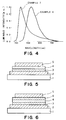
- FIG. 5 A description of a basic structure of an organic EL device is supplemented with reference to Figures 5 and 6 which illustrate organic EL devices including transparent substrates 1 and 2, a charge transporting layer 3, a luminescence layer 4, and a metal electrode 5 (and an electron transporting layer 6).
- an organic EL device generally includes a plurality of organic layers disposed between a transparent electrode 2 formed on a transparent substrate 1 and a metal electrode 5 disposed opposite to the transparent electrode 2.
- the organic layers comprise a luminescence layer 4 and a hole transporting layer 3.
- the transparent electrode 2 is composed of ITO (indium tin oxide), etc., having a relatively large work function so as to provide a good hole injection performance to the hole transporting layer 3.
- the metal electrode 5 is composed of a metallic material having a relatively small work function, such as aluminum, magnesium, or alloys of changing performance to the organic layers. These electrodes may have a thickness of 50 - 200 nm.
- the luminescence layer 4 may for example comprise an aluminum quinolinol complex (a representative example of which is Alq3 (tris(8-quinolinolato)aluminum) mentioned above and having a structure shown below).
- the hole transporting layer 3 may comprise an electron donative material, such as a triphenyldiamine derivative (representative examples of which may include ⁇ -NPD (bis[N-(1-naphthyl)-N-phenyl]benzidine) having a structure shown below.
- An organic EL device having an organization shown in Figure 5 exhibits a rectifying characteristic, and if an electric field is formed so that the metal electrode 5 forms a cathode and the transparent 2 forms an anode, electrons are injected into the luminescence layer 4 from the metal electrode, and holes are injected into the hole transporting layer 3 from the transparent electrode 2. The injected holes and electrons are re-combined in the luminescence layer 4 to generate excitons, thus causing luminescence.
- the hole transporting layer 3 functions as an electron blocking layer to increase the recombination efficiency at the luminance layer/hole transporting layer boundary, thus providing an increased luminance efficiency.
- an electron transporting layer 6 is disposed between the metal electrode 5 and the luminance layer 4 described with reference to Figure 5.
- the luminance function and the electron and hole transporting functions are separated to provide a more effective carrier blocking function, thereby allowing effective luminance.
- the electron transporting layer 6 may for example comprise an oxadiazole derivative.
- the organic (compound) layers may have a thickness on the order of 50 - 500 nm in total of the two or three layers.
- the above-mentioned conventional organic EL devices involve a problem that a short circuit is liable to occur between the electrodes since a high electric field of ca. 100 mV/cm is applied across thin layers in a thickness of ca. 100 nm.
- This problem can be alleviated to some extent by increasing the number of organic layers, but this can invite a problem in productivity.
- the reason why a high electric field on the order of 100 MV/cm is applied is because the carrier mobility of the organic layers is low, so that the applied electric field can be lowered, if the organic layers can be formed so as to exhibit a higher mobility.
- a carrier transporting layer generally used in a current organic EL device exhibits a mobility on the order of 10 -5 - 10 -3 cm 2 /V.sec, and a mobility on the order of 10 -3 cm 2 /V.sec is said to be a limit even by an amorphous material.
- the luminance efficiency is also affected by carrier injection performances from the electrodes.
- the carrier injection performance in the case of using an amorphous material is said to determine the luminance efficiency, and an amorphous material is not necessarily considered to be a material having a sufficient carrier injection performance.
- Such a conductive liquid crystal having a high carrier transporting performance may for example include a discotic liquid crystal and a smectic liquid crystal having a high degree of order.
- An organic layer in a conventional organic EL device has been of a monomeric amorphous type and has been formed by vacuum evaporation, so that it has been difficult to provide a thickness in excess of 1 ⁇ m in view of the productivity. Accordingly, the total thickness of the organic layers has generally been as thin as 100 nm - 200 nm, and this has been accompanied with several problems.
- the organic layers are thin, an electrical short circuit is liable to occur between the electrodes. Further, due to the necessity of carrier injection, an insulating layer cannot be inserted unlike in inorganic EL devices for obviating the above problem. As a result, the organic EL device has involved a problem regarding drive stability as an electronic device.
- the device capacitance is increased to cause a large drive current. This incurs an increase in power consumption and is not desirable.
- a high electric field (on the order of 10 V/100 nm) has been required for drive because of low performances of injection of electrons and holes from the electrodes, such as ITO, to the organic layers.
- organic materials used in an organic EL device has a band gap as broad as ca. 3.0 eV or more, thermal excitation-type free electrons are not present in a conduction band (or LUMO: Lowest Unoccupied Molecular Orbital), a drive current is principally supplied by a tunnel current injected from the electrodes.
- the injection efficiency of the current is known to be remarkably affected not only by the work functions of the electrodes and a level gap between LUMO and HOMO (Highest Occupied Molecular Orbital) of the organic materials but also by the molecular alignment and structure of the organic materials.
- LUMO and HOMO Highest Occupied Molecular Orbital
- minute crystalline boundaries function as carrier conduction obstacles, so that organic materials are generally used in an amorphous state, but only a low carrier injection efficiency is available in this case.
- an organic EL device is liable to be affected by invaded moisture to cause deterioration of luminance performance and drive performance, thus showing poor durability.
- the organic layers are disposed in lamination and then the cathode is formed thereon by vapor deposition of a metal film.
- a metal species having a small work function suitable for the cathode is susceptible of oxidation and has a low durability.
- the organic layers are liable to be degraded if the forming temperature is high (with an ordinary limit of 100 °C), and the destruction of the device structure due to the film stress is also problematic.
- a conductive liquid crystal layer formed by spin coating leaves problems regarding thickness uniformity, microscopic liquid crystal alignment uniformity and film uniformity.
- the alignment uniformity can be evaluated by the presence or absence of light leakage due to birefringence of the liquid crystal by observation through a cross nicol polarizing microscope.
- a conductive liquid crystal layer formed by spin coating is liable to involve portions of good alignment and poor alignment in mixture, and this may be attributable to ununiformity of vaporization of the solvent. Even if a liquid crystal layer is formed with little alignment irregularity by spin coating, it is difficult to provide satisfactory current and luminance performances.
- a Langmuir-Blodgett film is in a high-order state which is different from an amorphous state but is close to a crystal state, and may include crystal defects functioning as a carrier trap, thus leaving problems regarding the carrier transportation and luminance performances.
- a generic object of the present invention is to provide improvements to problems as mentioned above encountered in organic EL devices proposed heretofore.
- a more specific object of the present invention is to provide an organic EL device which requires a small power consumption and is excellent in reliability and durability.
- Another object of the present invention is to realize a carrier transporting layer exhibiting a high carrier injection efficiency from an electrode to organic layers, thus providing an organic EL device rich in durability by using thick organic layers including the carrier transporting layer.
- Another object of the present invention is to provide an organic EL device having a high reliability and including a carrier transporting layer or a luminance layer exhibiting a better performance by utilizing a liquid crystal compound having a high mobility.
- a further object of the present invention is to provide a conductive organic compound device and a conductive liquid crystal device having a structural feature common to an organic EL device satisfying the above objects.
- a conductive organic compound device comprising: a pair of oppositely spaced electrodes, and a carrier transporting layer disposed between the electrodes and in contact with one of the electrodes; wherein the carrier transporting layer comprises a conductive organic compound having a ⁇ -electron resonance structure in its molecule, and the ⁇ -electron resonance structure plane of the conductive organic compound in the carrier transporting layer is aligned substantially parallel to surfaces of the electrodes.
- the present invention further provides a conductive liquid crystal device obtained by using a conductive liquid crystal instead of the conductive organic compound in the above conductive organic compound device.
- an organic EL device comprising: a pair of oppositely spaced electrodes, and a carrier transporting layer and a luminescent organic layer disposed in lamination between the electrodes so that the carrier transporting layer is disposed in contact with one of the electrodes; wherein the carrier transporting layer comprises a conductive liquid crystal having a ⁇ -electron resonance structure in its molecule, and the ⁇ -electron resonance structure plane of the conductive liquid crystal in the carrier transporting layer is aligned substantially parallel to surfaces of the electrodes.
- a conductive liquid crystal device comprising: a pair of oppositely spaced electrodes, and at least one conductive liquid crystal layer formed by vacuum deposition of a conductive liquid crystal and assuming a liquid crystal state and an amorphous layer formed by vacuum deposition of a conductive organic compound and contacting the conductive liquid crystal layer, respectively disposed between the electrodes.
- an organic electroluminescence device By using either one of the conductive liquid crystal layer and the amorphous layer as a luminescence layer, there is also provided an organic electroluminescence device.
- the organic EL device of the present invention By using the conductive organic compound device or the conductive liquid crystal device having a carrier transporting layer exhibiting a high carrier injection efficiency, it is possible to constitute an electronic device requiring a reduced power consumption. According to the organic EL device of the present invention, the total thickness of the organic layers including the conductive liquid crystal layer can be increased, so that it is possible to provide a reliable EL device. Further, by forming a cell structure including a glass substrate, etc., it is possible to provide an EL device having a high durability.
- a device structure including an amorphous layer in addition to a conductive liquid crystal layer, it becomes possible to more effectively utilize the high carrier mobility characteristic of the conductive liquid crystal layer, thus further increasing the reliability. Accordingly, it is possible to provide an organic EL device having a high luminance intensity at a lower voltage. Because of the lower voltage, the short circuit between the electrodes is less liable to occur, thus improving the reliability also in this respect.
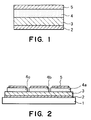
- Figure 1 is a schematic sectional view for illustrating a basic structure of an organic EL device according to an embodiment of the invention.
- Figure 2 is a schematic sectional view of an organic EL device prepared in an Example of the invention.
- Figures 3A and 3B are graphs showing a voltage-current characteristic and a temperature-dependence of current, respectively, of the organic EL device of Example 4.
- Figure 4 is a graph showing luminance spectra of organic EL devices of some Examples.
- Figures 5 and 6 are respectively a schematic sectional view of a known organic EL device.
- an (electro)conductive organic compound having a ⁇ -electron resonance structure in its molecule is used to form a carrier transporting layer wherein the ⁇ -electron resonance structure plane of the conductive organic compound is aligned in substantially parallel to an associated electrode surface, thereby improving the carrier injection performance from the electrode boundary.
- a conductive organic compound device particularly a conductive liquid crystal device using a conductive liquid crystal as the conductive organic compound, including such a carrier transporting layer, can be applied to electronic devices, such as a photo-sensor, a photoconductor (for constituting, e.g., a photosensitive drum for copying machines), an organic semiconductor device (such as an organic TFT (thin film transistor)), a temperature sensor, and a spatial modulation device, and particularly preferably to an organic EL device.
- electronic devices such as a photo-sensor, a photoconductor (for constituting, e.g., a photosensitive drum for copying machines), an organic semiconductor device (such as an organic TFT (thin film transistor)), a temperature sensor, and a spatial modulation device, and particularly preferably to an organic EL device.
- electronic devices such as a photo-sensor, a photoconductor (for constituting, e.g., a photosensitive drum for copying machines), an organic semiconductor device (such as an organic TFT (th
- a conductive liquid crystal is used as the conductive organic compound for constituting a carrier transporting layer, it becomes easy to align the ⁇ -electron resonance plane thereof parallel to the associated electrode surface.
- the conductive liquid crystal aligned in this manner can take advantage of the following effects.
- the ⁇ -electron resonance structure plane of the conductive organic compound (or the conductive liquid crystal compound) is required to be aligned substantially parallel to the electrode surfaces. This is satisfied not only where the ⁇ -electron resonance structure plane is completely parallel to the electrode surfaces but also where the resonance structure plane is aligned with some insubstantial inclination angle, i.e., below 45 deg. at the maximum, from the extension of the surface of one of the opposite electrodes disposed closer to the conductive organic compound (or liquid crystal) layer.
- a conductive liquid crystal layer formed by vacuum deposition is used for providing a high-performance device, particularly an organic EL device. According this embodiment, it is possible to take advantage of the following effects attributable to the vacuum deposition scheme in general.
- the organic EL device according to the present invention can have basically similar organizations as shown in Figures 5 and 6 of conventional organic EL devices. Further, the organic EL device can comprise a transparent substrate 1, a transparent electrode 2 and a metal electrode 5 which are similar in structure and can comprise similar materials as the corresponding members described with reference to Figures 5 and 6.
- the ⁇ -electron resonance structure of the conductive organic compound or the conductive liquid crystal constituting the carrier transporting layer is generally given by an aromatic ring, examples thereof may include: triphenylene ring, naphthalene ring and benzene ring, as representative, and also pyridine ring, pyrimidine ring, pyridazine ring, pyrazine ring, tropone ring, azulene ring, benzofuran ring, indole ring, indazole ring, benzothiazole ring, benzoxazole ring, benzimidazole ring, quinoline ring, isoquinoline ring, quinazoline ring, quinoxaline ring, phenanthrene ring and anthracene ring.
- the conductive liquid crystal used in the present invention may preferably comprise a discotic i liquid crystal or a smectic liquid crystal.
- a discotic liquid crystal may generally have a core structure which may be given by an aromatic ring as mentioned above for the ⁇ -electron resonance structure, as represented by triphenylene ring (or skeleton). Further examples thereof may include truxene skeleton, metal-phthalocyanine skeleton, phthalocyanine skeleton, dibenzopyrene skeleton, metal-phthalocyanine skeleton, dibenzopyrene skeleton, and hexabenzocoronene skeleton.
- the discotic liquid crystal used in the present invention may preferably be a liquid crystal having a discotic disordered phase or a liquid crystal phase having a lower order than the discotic disordered phase. More specifically, it is preferred to use a liquid crystal having a discotic disordered phase or a discotic nematic phase.
- Examples of the discotic liquid crystal may include LC Compounds 1 - 5 represented by the following structural formulae (as shown in Advanced Materials, 1996, 8, No. 10).
- LC compounds 1 - 4 having side chains of thioether group (-SC 6 H 13 ) or alkoxy groups (-OC 4 H 9 , etc.) are known to have a hole-transporting characteristic at a high mobility (10 -1 - 10 -3 cm 2 /V.sec).
- Each of these compounds has a discotic columnar phase, and disk-shaped molecules thereof are aligned so as to form columns and so that triphenylene skeletons thereof having abundant ⁇ -electron planes are mutually overlapped, whereby it is possible to attain a good hole-transporting performance via the triphenylene skeletons.
- the discotic liquid crystal phases may be classified into discotic nematic phase and discotic columnar phase, and the discotic columnar phase is further divided into discotic disordered phase and discotic ordered phase which has a higher order than the discotic disordered phase.
- a higher mobility is exhibited by a liquid crystal having discotic ordered phase, but in view of a carrier injection performance from an electrode surface, a liquid crystal having discotic disordered phase can exhibit a better performance because of its better alignability of ⁇ -electron resonance plane parallel to the electrode surface according to the present invention, thus being preferably used to constitute a carrier transporting layer according to the present invention.
- the carrier injection is effected by a tunnel current or a Schottky current depending on an energy barrier at the injection boundary.
- the current is flowed as a spatial charge controlling current proportional to the mobility. Accordingly, in order to perform an effective current flow, it is preferred to improve the injection performance at a proximity to the boundary and use a material having an internally large mobility.
- a discotic liquid crystal for a carrier transporting layer
- a two layer-structured liquid crystal layer including a lamination of a layer of discotic liquid crystal showing discotic disordered phase at the boundary with the electrode and a layer of discotic liquid crystal showing discotic ordered phase on a remoter side from the electrode.
- HBOT hexabisbutyloxytriphenylene
- the smectic liquid crystal used in the present invention may preferably be a smectic liquid crystal having SmE phase or a smectic phase of a lower order than SmE phase. More specifically, it is preferred to use a liquid crystal having SmE phase or SmB phase.
- a smectic liquid crystal having SmE phase PN84 (2-butoxy-6-(3-octylphenyl)naphthalene) may for example be preferably used.
- Examples of other smectic liquid crystals may include LC Compounds 6 and 7 represented by structural formulae shown below (as disclosed in Ohyou Butsuri (Applied Physics), Vol. 68, No. 1, p. 26- (1999)).
- LC Compound 6 is a phenylbenzothiazole derivative having SmA phase and has a hole-transporting characteristic.
- LC Compound 7 is a phenylnaphthalene derivative having SmA phase and SmE phase (higher order phase) and showing a higher mobility in the SmE phase, and shows a bipolar transporting characteristic of transporting both holes and electrons.
- liquid crystal compounds having a bar-shaped structure.
- an amorphous layer formed by vacuum deposition of an organic compound in lamination with the conductive liquid crystal layer it is possible to use either one of the conductive liquid crystal layer and the amorphous layer as a luminance layer.
- Examples of the organic compound constituting the amorphous layer in the present invention may include known luminescence materials and carrier-transporting materials inclusive of Alq3 and ⁇ -NPD mentioned above and compounds disclosed in Macromol. Symp. 125, pp. 1 - 48 (1997).
- the carrier transporting layer of a conducive liquid crystal according to the present invention may be formed by vacuum deposition on an electrode.
- the layer of conductive liquid crystal after the vacuum deposition is assumed to have an amorphous state, i.e., isotropic, indefinite and bulky alignment state. Liquid crystal molecules in such an alignment state can readily cause an alignment change at a liquid crystal phase temperature. Accordingly, in a device including a carrier transporting layer formed by vacuum deposition of a conductive liquid crystal, it is possible to easily re-align the ⁇ -electron resonance phase parallel to an associated electrode surface by an appropriate heating treatment, thereby attaining a high carrier injection efficiency.
- examples of the anode materials may include: indium oxide, tin oxide, Cd 2 SnO 4 , zinc oxide, copper iodide, gold and platinum, in addition to ITO.
- examples of the cathode materials may include: alkali metals, alkaline earth metals and alloys of these, inclusive of sodium, potassium, magnesium, lithium, sodium-potassium alloy, magnesium-indium alloy, magnesium-silver alloy, aluminum, aluminum-lithium alloy, aluminum-copper alloy, aluminum-copper-silicon alloy.
- examples of materials for the luminescent organic layer may include: in addition to Alq3, BeBq (bis(benzoquinolinolato)beryllium), DTVB2 (4,4'-bis(2,2-di-p-tolylvinyl)biphenyl), Eu(DBM)3(Phen)(tris(1,3-diphenyl-1,3-propanediono)monophenanthroline)Eu(III)), and further, diphenylethylene derivatives, triphenylamine derivatives, diaminocarbazole derivatives, bisstyryl derivatives, benzothiazole derivatives, benzoxazole derivatives, aromatic diamine derivatives, quinacridone compounds, perylene compounds, oxadiazole derivatives, coumarin compounds, and anthraquinone derivatives. These materials are preferably formed in an amorphous state by vacuum deposition.
- FIG. 1 is a schematic sectional view showing a basic structure of an embodiment of the organic EL device according to the present invention.
- the organic EL device includes an anode 2, a carrier transporting layer 3, a luminescent organic layer 4 and a cathode 5, laminated in this order.
- the carrier transporting layer 3 comprises a hole-transporting conductive liquid crystal having HOMO close to the energy level of ITO constituting the anode 2 and is disposed in contact with the anode 2.
- a carrier transporting layer comprising a conductive liquid crystal having an electron-transporting characteristic and disposed in contact with the cathode 5 is expected to have a similar effect of improving the carrier injection from the electrode.
- FIG. 2 shows a similar structure as in Figure 1 but shows a glass substrate 1 supporting the anode 2 and luminance layers 4a, 4b and 4c of different colors instead of the single luminance layer 4 in Figure 1.
- a 70 nm-thick ITO film was formed as a hole-injecting anode 2 by sputtering using a target of In 90 % and Sn 10 % while flowing Ar gas at 200 sccm and O 2 gas at 3 sccm.
- the ITO film showing a work function of ca. 4.35 eV was exposed to ultraviolet rays from a low-pressure mercury lamp to have an elevated work function of 4.60 eV.
- HHOT hexabishexyloxytriphenylene
- the above-treated substrate 1 having an ITO film 2 was placed in a vacuum chamber held at a pressure below 2x10 -5 torr, and a ca. 50 nm-thick layer of HHOT (hexabishexyloxytriphenylene) was formed on the ITO film 2 as a carrier transporting layer 3 by vacuum deposition at a rate of ca. 0.1 nm/sec at a pressure of 1x10 -5 torr according to the resistance heating vacuum deposition method.
- HHOT exhibited a mobility of 1x10 -3 cm 2 /V.sec at ca. 70 °C or below according to the time-of-flight method when sandwiched in a 15 ⁇ m-thick layer between a pair of ITO substrates.
- HHOT is a discotic liquid crystal causing a transition from crystal to discotic disordered phase at 65 °C and a transition to isotropic phase at 98 °
- Luminescent organic layer segments 4a - 4c exhibiting different luminescent wavelengths were respectively formed in a thickness of 50 nm on the HHOT layer 3 by vacuum deposition through a mask under the conditions of a pressure of 1x10 -5 torr and a deposition rate of ca. 0.1 mm/sec.
- the organic layers 4a - 4c were respectively formed of Alq3 alone, Alq3 doped with 5 wt. % of perylene for shifting the luminescence wavelength to a shorter wavelength side, and Alq3 doped with 5 wt. % of DCM (a styryl dye) for shifting to a longer wavelength side.
- DCM a styryl dye
- the device was heated to 65 °C, whereby electroluminescence was realized at an increased current at that temperature.
- the liquid crystal in the carrier transporting layer 3 on the ITO electrode 2 was aligned so that the discotic columns thereof were aligned substantially vertical to the electrode surface.
- the liquid crystal alignment was confirmed by using a sample device having a layer structure of ITO (70 nm)/HHOT (50 nm)/Alq3 (10 nm)/Al (10 nm) and observing it though a right-angle cross nicol polarizing microscope, whereby the vertical alignment of discotic columns was confirmed from a uniformly dark view of the device. This indicates that the ⁇ -electron resonance planes of the liquid crystal molecules were aligned substantially parallel to the electrode surfaces. A similar alignment was confirmed also when the HHOT layer thickness was increased to 150 nm. The thus-formed parallel ⁇ -electron plane alignment is believed to have caused an increased interaction with electron cloud at the ITO surface, thereby promoting the hole injection.)
- a 70 nm-thick ITO film was formed by sputtering similarly as in Example 1 and then subjected to an oxygen-plasma treatment under the conditions of O 2 gas flow rate of 200 sccm, a pressure of 10 m.torr, a power of 400 W and a treatment time of 4 min., whereby the ITO film was caused to have an elevated work function of ca. 4.93 eV.
- the above-treated substrate having an ITO film was coated with a carrier transporting layer comprising a lamination of a 20 nm-thick HHOT layer and a 50 nm-thick HBOT layer.
- the HHOT layer and the HBOT layer were respectively formed by the resistance heating vacuum deposition method at a pressure of 1x10 -5 torr and a deposition rate of ca. 0.1 mm/sec successively in the same vacuum chamber with an intermediate re-evacuation step.
- HBOT exhibited a mobility of 1x10 -2 cm 2 /V.sec at ca. 70 °C or below according to the time-of-flight method.
- HBOT is a discotic liquid causing a transition from crystal to discotic ordered phase at 89.4 °C and a transition to isotropic phase at 144.7 °C.
- luminescent organic layers 4a - 4c and cathode metals 5 were formed in the carrier transporting layer 3 similarly as in Example 1 to obtain an organic EL device.
- the device was heated to 75 °C, whereby electroluminescence was realized at an increased current at that temperature.
- An organic EL device was prepared in the same manner as in Example 2 except that a carrier transporting layer was formed on the ITO layer by first forming a 20 nm-thick HBOT layer and then forming a 50 nm-thick HHOT layer thereon.
- a glass substrate was coated with an ITO film and treated by UV treatment in the same manner as in Example 1.
- the ITO film on the substrate was further coated with a carrier transporting layer comprising in lamination a 20 nm-thick layer of CuPc (copper-phthalocyanine) having a structure represented by a formula below and a 50 nm-thick layer of HHOT respectively formed by vacuum deposition under conditions similar to those adopted for the vacuum deposition of the HHOT layer in Example 1.
- a carrier transporting layer comprising in lamination a 20 nm-thick layer of CuPc (copper-phthalocyanine) having a structure represented by a formula below and a 50 nm-thick layer of HHOT respectively formed by vacuum deposition under conditions similar to those adopted for the vacuum deposition of the HHOT layer in Example 1.
- luminescent organic layers 4a - 4c and cathode metals 5 were formed on the carrier transporting layer 3 similarly as in Example 1 to obtain an organic EL device.
- Example Layer structure Temp The above-prepared 4 devices of Examples 1 - 2 and Comparative Examples 1 - 2 were respectively supplied with an electric field of 12 V/100 nm at various temperatures (30 °C and a liquid crystal phase temperature) to measure a current density. The results are inclusively shown in Table 1 below.
- Example Layer structure Temp Example Layer structure Temp.
- Example 1 As is shown in Table 1 above, the device of Example 1 exhibited only a low current density of 50 ⁇ A/cm 2 at 30 °C (crystal phase temperature for HHOT) where HHOT was presumably in an amorphous state after the vacuum deposition, but exhibited a remarkably increased current density of 3593 ⁇ A/cm 2 when heated to 65 °C (to 68 °C) where it was confirmed that HHOT was placed in discotic disordered phase and in a homeotropic alignment state where the director (defined as a vector perpendicular to a ⁇ -electron resonance plane of a core of a discotic liquid crystal) of HHOT was perpendicular to the ITO film between the ITO film and the Alq3 film.
- the director defined as a vector perpendicular to a ⁇ -electron resonance plane of a core of a discotic liquid crystal
- a discotic liquid crystal has a negative refractive index anisotropy, so that no phase difference is formed in a direction perpendicular to the electrode surface when the discotic liquid crystal is placed in the homeotropic alignment state where the above-defined director is aligned normal to the electrode surface. For this reason, an alignment state of a discotic liquid crystal can be specified through a polarizing microscope observation.
- Comparative Example 1 exhibited a current density of 140 ⁇ A/cm 2 at 30 °C somewhat higher than the device of Example 1. This is presumably because HBOT having a mobility higher by one digit than HHOT was used in Comparative Example 1.
- the device of Comparative Example 1 did not exhibit a remarkable increase in current density unlike the device of Example 1 when heated to 90 °C. This is presumably because HBOT assumes discotic ordered phase at 90 °C and does not have discotic disordered phase.
- HHOT assumes a homeotropic alignment state wherein the director is aligned in agreement with a normal to the substrate as mentioned above, whereas HBOT does not readily assume a homeotropic alignment state but assumes a substantially random alignment state.
- Example 2 caused a remarkable increase in current density similarly as in Example 1 when heated to 65 °C. This may be attributable to an improvement in carrier injection efficiency at the boundary between the ITO film and the HHOT layer due to alignment of HHOT.
- the increase in current density was observed in some cases even at a temperature somewhat below the phase transition temperature (65 °C) where the liquid crystal portion was not considered to completely form a homeotropic alignment. This may be attributable to a feature that a microscopic alignment change favoring the improvement in carrier injection at the electrode boundary can be relatively easily caused in discotic disordered phase.
- the device of Comparative Example 2 including a 20 nm-thick CuPc layer inserted between the ITO electrode and the HHOT layer exhibited a remarkably larger current density of 1136 ⁇ A/cm 2 .
- CuPc has a HOMO of 4.09 eV lower than an HHOT's HOMO of 5.13 eV and provided a reduced energy barrier of 0.09 eV reduced from 0.53 eV relative to the ITO's work function of 4.60 eV.
- the device of Comparative Example 2 did not cause a substantial increase in current density even when heated to 65 - 68 °C. This is presumably because CuPc have no liquid crystal phase is a temperature range of 65 - 68 °C, and a carrier injection efficiency improvement by re-alignment of ⁇ -electron resonance plane as in the device of Example 1 cannot be expected.
- An organic EL device was prepared in the same manner as in Example 1 except that a 50 nm-thick layer of PN84 (a bar-shaped smectic liquid crystal) was formed by vacuum deposition instead of the HHOT layer under the conditions of a pressure of 1x10 -5 torr and a deposition rate of ca. 0.1 nm/sec.
- PN84 a bar-shaped smectic liquid crystal
- PN84 causes a phase transition from crystal phase to SmE phase (liquid crystal phase) at 68.7 °C, a phase transition from SmE phase to SmA phase (liquid crystal phase), and a phase transition of SmA phase to isotropic phase at 131.1 °C, and also exhibits a mobility of ca. 10 -3 cm 2 /V.sec in SmE phase.
- PN84 assumed a homogeneous alignment state wherein the director thereof was aligned parallel to the ITO electrode surface but in random directions between the ITO electrode and the Alq3 layer.
- a director is taken in a molecular long-axis direction so that the director alignment in the carrier transporting layer parallel to the electrode surface provides an organic EL device wherein the ⁇ -electron resonance plane of the liquid crystal is aligned parallel to the electrode surface.
- a 1.1 mm-thick glass substrate was coated by sputtering with a 50 nm-thick ITO layer, which was surface-cleaned by irradiation with ultraviolet rays.
- HHOT hexakis(hexyloxy)triphenylene
- the Alq3 layer was further coated first with a 10 nm-thick layer of Al-Li alloy (Li 1.8 wt. %) and then with a 150 nm-thick Al layer.
- the two-layer electrode structure was adopted so as to protect with the Al electrode the Al-Li alloy which has a low work function and a high electron injection performance while showing a poor stability because of a high reactivity with the atmosphere, etc.
- the device exhibited a voltage (V) - current (I) characteristics at 30 °C and 70 °C as shown in Figure 3A.
- Luminance was confirmed by the device in a initial state (at 30 °C), i.e., before heating to the liquid crystal phase temperature.
- the liquid crystal compound HHOT was formed in an amorphous layer by the vacuum deposition method, so that the device was assumed to exhibit a V-I characteristic corresponding to an electrical property in the amorphous state.
- the HHOT layer showed a hole-transporting characteristic even in the amorphous state.
- HHOT shows Dhd phase (discotic hexagonal disordered phase) within a liquid crystal temperature range of 69 - 99 °C in the course of temperature increase.
- the device exhibited a remarkable current increase when heated to 70 °C. This is presumably because the molecular alignment in the HHOT layer was transformed into Dhd phase by heating to a liquid crystal phase temperature and the hole-transporting performance of the HHOT layer was increased inclusive of hole-injecting performance from the electrode.
- Figure 3B shows a temperature-dependent current characteristic of the device at a fixed applied voltage of 12 volts.
- Figure 3B clearly shows an abrupt increase in current in the vicinity of the phase transition temperature into a liquid crystal phase.
- a dramatic improvement by molecular re-alignment in the liquid crystal phase is indicated.
- Green electroluminescence from Alq3 was confirmed while showing a nearly proportional relationship between the current and luminous intensity. This means that the increased current characteristic provided the increased EL luminescence performance.
- the alignment characteristic of the liquid crystal in the device was examined by observation through a polarizing optical microscope.
- a sample device having a layer structure of ITO (50 nm)/HHOT (200 nm)/Alq3 (50 nm) was prepared because such an optical microscope examination preferred a liquid crystal layer thickness of at least 200 nm and the absence of a metal electrode.
- the Alq amorphous layer does not show birefringence, so that the alignment of HHOT can be examined by observation of the device through a cross nicol polarizing microscope.
- the region of HHOT above i.e., free from coverage with Alq3 was also formed in the device.
- the results of the examination are shown in the following Table 2. Alignment Layer structure room temp. (crystal) 70 °C (Dhd phase) HHOT alone random random HHOT/Alq3 random homeotropic (dark view)
- the HHOT layer formed by vacuum deposition in contact with an amorphous Alq3 layer assumed a homeotropic alignment state at a liquid crystal phase temperature.
- the random state of HHOT and the homeotropic state of HHOT could be easily differentiated because the former caused light leakage and the latter provided a uniform state free from light leakage as a result of observation through the polarizing microscope.
- An organic EL device was prepared in the same manner as in Example 4 except that a 50 nm-thick layer of the discotic liquid crystal compound HHOT was formed by spin coating instead of the vacuum deposition.
- a glass substrate coated with an ITO film identical to the one prepared in Example 4 was coated with a 1 wt. % HHOT solution in chloroform (CHCl 3 ) by spin coating at 2000 rpm for 20 sec, followed by drying to form a 50 nm-thick HHOT layer.
- CHCl 3 chloroform
- the HHOT layer was then successively coated with an Alq3 layer, an Al-Li layer and an Al layer respectively by vacuum deposition in the same manner as in Example 4.
- the thus-obtained device was subjected to measurement of V-I characteristic in the same manner as in Example 4.
- the device Under application of an identical voltage of 10 volts at an identical liquid crystal phase temperature of 70 °C, the device exhibited a current value of ca. 1/15 and a luminous intensity of ca. 1/20, respectively, of those of the device of Example 4.
- An organic EL device including three organic compound layers was prepared. More specifically, an ITO film formed on a glass substrate identical to the one in Example 4 was successively coated with a 20 nm-thick layer of ⁇ -NPD, a 50 nm-thick layer of the above-mentioned discotic LC Compound 5 (cyclohexanecarboxylic acid-3,6,7,10,11-pentakispentyloxytriphenylene-2-yl-ester) and a 50 nm-thick layer of Alq3 respectively by vacuum deposition under similar conditions as in Example 4.
- a 20 nm-thick layer of ⁇ -NPD a 50 nm-thick layer of the above-mentioned discotic LC Compound 5 (cyclohexanecarboxylic acid-3,6,7,10,11-pentakispentyloxytriphenylene-2-yl-ester) and a 50 nm-thick layer of Alq3 respectively by vacuum deposition
- LC Compound 5 is a discotic liquid crystal compound showing a liquid crystal phase at 189 °C or below including Dhd phase (discotic hexagonal ordered phase) at room temperature. Then, an Al-Li layer and an Al layer were formed thereon in the same manner as in Example 4.
- the thus-prepared device also showed good rectifying performance causing electroluminescence.
- Example 4 the alignment characteristic of LC Compound 5 in the device was examined by preparing a sample device having a layer structure of ITO (50 nm)/ ⁇ -NPO (20 nm)/LC Compound 5 (200 nm)/Alq3 (50 nm). As a result, it was confirmed that LC Compound 5 was placed in a good homeotropic alignment state free from light leakage by observation under cross nicols at the liquid crystal phase temperature.
- an ITO electrode formed on a glass substrate identical to the one formed in Example 4 was successively coated with a 50 nm-thick hole-transporting layer of ⁇ -NPD, a 50 nm-thick luminescence layer of Alq3 and a 50 nm-thick layer of PN84, respectively by vacuum deposition under similar conditions as in formation of the HHOT and Alq3 in Example 4.
- PN84 is a liquid crystal compound showing bipolar carrier-transporting characteristics, but was used for constituting an electrode-transporting layer, PN84 shows a liquid crystal phase in a temperature range of 55 - 129 °C.
- the alignment characteristic of the liquid crystal PN84 was examined by preparing a sample device having a layer structure of ITO (50 nm)/ ⁇ -NPD (50 nm)/Alq3 (50 nm)/PN84 (200 nm). As a result, it was confirmed that PN84 was in a random alignment with no directionality at room temperature, and in a substantially homogeneous alignment on the Alq3 layer at a liquid crystal phase temperature. Accordingly, in the device of this Example, it was understood that the smectic liquid crystal PN84 was in a homogeneous alignment state showing a good carrier transportation characteristic at a liquid crystal phase temperature.
- the electrodes were similar to those formed in Example 4.
- the organic EL device exhibited a good rectifying performance.
- blue luminescence was confirmed while the luminance intensity was weaker than the device of Example 4 using Alq3.
- the luminance spectra of the devices of Example 4 using Alq3 and Example 8 using PN84 are shown in Figure 4.
- PN84 was excited with ultraviolet rays to examine photoluminescence, as a luminance spectrum substantially similar to the one shown in Figure 4, the luminescence of the device of this Example 8 was identified as luminance from PN84.
- the current was increased to three times and the luminous intensity was increased to ca. 2.5 times respectively compared to those at 30 °C.
Landscapes
- Chemical & Material Sciences (AREA)
- Physics & Mathematics (AREA)
- Engineering & Computer Science (AREA)
- Materials Engineering (AREA)
- Optics & Photonics (AREA)
- Crystallography & Structural Chemistry (AREA)
- Spectroscopy & Molecular Physics (AREA)
- Electroluminescent Light Sources (AREA)
- Organic Low-Molecular-Weight Compounds And Preparation Thereof (AREA)
Applications Claiming Priority (4)
| Application Number | Priority Date | Filing Date | Title |
|---|---|---|---|
| JP25500799 | 1999-09-09 | ||
| JP25500799 | 1999-09-09 | ||
| JP27387899 | 1999-09-28 | ||
| JP27387899 | 1999-09-28 |
Publications (2)
| Publication Number | Publication Date |
|---|---|
| EP1083613A2 true EP1083613A2 (de) | 2001-03-14 |
| EP1083613A3 EP1083613A3 (de) | 2006-04-05 |
Family
ID=26541970
Family Applications (1)
| Application Number | Title | Priority Date | Filing Date |
|---|---|---|---|
| EP00307698A Withdrawn EP1083613A3 (de) | 1999-09-09 | 2000-09-07 | Leitende organische Verbindung mit einer pi-Elektronen-Resonanzstruktur |
Country Status (2)
| Country | Link |
|---|---|
| US (1) | US6858271B1 (de) |
| EP (1) | EP1083613A3 (de) |
Cited By (5)
| Publication number | Priority date | Publication date | Assignee | Title |
|---|---|---|---|---|
| EP1089596A3 (de) * | 1999-09-28 | 2003-02-05 | Canon Kabushiki Kaisha | Leitende Flüssigkristallvorrichtung und organische elektrolumineszente Vorrichtung |
| WO2003056880A3 (fr) * | 2001-12-24 | 2004-02-12 | Saint Gobain | Vitre feuilletee avec un element fonctionnel a commande electrique |
| GB2405260A (en) * | 2003-07-29 | 2005-02-23 | Dainippon Printing Co Ltd | Organic electroluminescent element |
| US6870583B2 (en) | 2000-04-07 | 2005-03-22 | Canon Kabushiki Kaisha | Conductive liquid crystal device and organic electroluminescence device |
| CN100435382C (zh) * | 2004-08-13 | 2008-11-19 | 胜华科技股份有限公司 | 偏极化电激发光面板及其制作方法 |
Families Citing this family (11)
| Publication number | Priority date | Publication date | Assignee | Title |
|---|---|---|---|---|
| US20010048982A1 (en) * | 2000-04-28 | 2001-12-06 | Tohoku Pioneer Corporation | Organic electroluminescent display device and chemical compounds for liquid crystals |
| US7301279B2 (en) * | 2001-03-19 | 2007-11-27 | Semiconductor Energy Laboratory Co., Ltd. | Light-emitting apparatus and method of manufacturing the same |
| US6699597B2 (en) * | 2001-08-16 | 2004-03-02 | 3M Innovative Properties Company | Method and materials for patterning of an amorphous, non-polymeric, organic matrix with electrically active material disposed therein |
| US7045861B2 (en) * | 2002-03-26 | 2006-05-16 | Semiconductor Energy Laboratory Co., Ltd. | Light-emitting device, liquid-crystal display device and method for manufacturing same |
| JP2004355813A (ja) * | 2003-05-27 | 2004-12-16 | Tohoku Pioneer Corp | 自発光表示装置およびこれを用いた情報機器 |
| US7902747B2 (en) * | 2003-10-21 | 2011-03-08 | Semiconductor Energy Laboratory Co., Ltd. | Light-emitting device having a thin insulating film made of nitrogen and silicon and an electrode made of conductive transparent oxide and silicon dioxide |
| JP2005166265A (ja) * | 2003-11-28 | 2005-06-23 | Hitachi Displays Ltd | 有機el表示装置 |
| JP2008518446A (ja) * | 2004-10-25 | 2008-05-29 | ザ リージェンツ オブ ザ ユニバーシティー オブ カリフォルニア | 有機電子デバイス用積層電極 |
| US8059658B1 (en) | 2005-12-23 | 2011-11-15 | Extreme Networks, Inc. | Method and system for automatic expansion and contraction of IP host forwarding database |
| US9123902B2 (en) * | 2011-02-10 | 2015-09-01 | Samsung Electronics Co., Ltd. | Semiconductor compound |
| US9123899B2 (en) * | 2011-02-10 | 2015-09-01 | Samsung Electronics Co., Ltd. | Semiconductor compound |
Family Cites Families (9)
| Publication number | Priority date | Publication date | Assignee | Title |
|---|---|---|---|---|
| DE4445584A1 (de) * | 1994-12-20 | 1996-06-27 | Basf Ag | Verwendung von organischen Materialien hoher nichtionischer Ladungsträgerbeweglichkeit |
| US5858273A (en) * | 1995-07-27 | 1999-01-12 | Canon Kabushiki Kaisha | Liquid crystal device |
| US6017470A (en) * | 1995-08-21 | 2000-01-25 | The Trustees Of Columbia University In The City Of New York | Substituted [6]helicene compounds that show enhanced nonlinear optical rotatory power and uses thereof |
| US5766510A (en) * | 1995-08-25 | 1998-06-16 | Dai Nippon Printing Co., Ltd. | Liquid crystalline compound and use thereof |
| WO1997018944A1 (en) * | 1995-11-22 | 1997-05-29 | The Government Of The United States Of America, Represented By The Secretary Of The Navy | Patterned conducting polymer surfaces and process for preparing the same and devices containing the same |
| US6150042A (en) * | 1996-12-09 | 2000-11-21 | Toyo Ink Manufacturing Co., Ltd. | Material for organoelectro-luminescence device and use thereof |
| JP3524404B2 (ja) * | 1998-10-05 | 2004-05-10 | キヤノン株式会社 | ディスコティック液晶素子および配向方法 |
| JP3472189B2 (ja) * | 1999-04-08 | 2003-12-02 | キヤノン株式会社 | キャリア輸送素子及び発光素子 |
| EP1089596A3 (de) * | 1999-09-28 | 2003-02-05 | Canon Kabushiki Kaisha | Leitende Flüssigkristallvorrichtung und organische elektrolumineszente Vorrichtung |
-
2000
- 2000-09-07 US US09/656,942 patent/US6858271B1/en not_active Expired - Fee Related
- 2000-09-07 EP EP00307698A patent/EP1083613A3/de not_active Withdrawn
Cited By (8)
| Publication number | Priority date | Publication date | Assignee | Title |
|---|---|---|---|---|
| EP1089596A3 (de) * | 1999-09-28 | 2003-02-05 | Canon Kabushiki Kaisha | Leitende Flüssigkristallvorrichtung und organische elektrolumineszente Vorrichtung |
| US6870583B2 (en) | 2000-04-07 | 2005-03-22 | Canon Kabushiki Kaisha | Conductive liquid crystal device and organic electroluminescence device |
| WO2003056880A3 (fr) * | 2001-12-24 | 2004-02-12 | Saint Gobain | Vitre feuilletee avec un element fonctionnel a commande electrique |
| US7009156B2 (en) | 2001-12-24 | 2006-03-07 | Saint-Gobain Glass France | Laminated glass plane with electrically controlled functional element |
| CZ307923B6 (cs) * | 2001-12-24 | 2019-08-21 | Saint-Gobain Glass France | Vrstvená okenní tabule s elektricky ovládaným funkčním prvkem |
| GB2405260A (en) * | 2003-07-29 | 2005-02-23 | Dainippon Printing Co Ltd | Organic electroluminescent element |
| GB2405260B (en) * | 2003-07-29 | 2006-07-19 | Dainippon Printing Co Ltd | Organic electroluminescent element and method for producing the same |
| CN100435382C (zh) * | 2004-08-13 | 2008-11-19 | 胜华科技股份有限公司 | 偏极化电激发光面板及其制作方法 |
Also Published As
| Publication number | Publication date |
|---|---|
| US6858271B1 (en) | 2005-02-22 |
| EP1083613A3 (de) | 2006-04-05 |
Similar Documents
| Publication | Publication Date | Title |
|---|---|---|
| Hohnholz et al. | Applications of phthalocyanines in organic light emitting devices | |
| JP4144192B2 (ja) | 有機電界発光素子の製造方法 | |
| JP4058842B2 (ja) | 有機電界発光素子 | |
| US7037599B2 (en) | Organic light emitting diodes for production of polarized light | |
| JP4023204B2 (ja) | 有機電界発光素子 | |
| US6858271B1 (en) | Conductive organic compound device, conductive liquid crystal device, and organic electroluminescence device | |
| WO1999053724A1 (en) | Color-tunable organic light emitting devices | |
| EP1175470A4 (de) | Elektronische vorrichtung, die eine organische substanz mit p-typ halbleitereigenschaften enthält. | |
| JPWO1998008360A1 (ja) | 有機el素子 | |
| JPWO1998030071A1 (ja) | 有機el素子 | |
| KR20050085239A (ko) | 유기 전자발광 부품 | |
| US8293385B2 (en) | Organic electronic devices using phthalimide compounds | |
| Chiu et al. | Bisindolylmaleimides as red electroluminescence materials | |
| Chen et al. | Light-emitting organic materials with variable charge injection and transport properties | |
| US6528940B1 (en) | Conductive liquid crystal device, and organic electroluminescence device | |
| JP2848189B2 (ja) | 有機薄膜el素子 | |
| JP2000150169A (ja) | 有機電界発光素子 | |
| US6870583B2 (en) | Conductive liquid crystal device and organic electroluminescence device | |
| JP2000252077A (ja) | 有機エレクトロルミネッセンス素子 | |
| US6788361B2 (en) | Electro-conductive liquid crystal element and organic electro-luminescence element | |
| EP1104036A2 (de) | Flüssigkristallanordnung | |
| JP3471910B2 (ja) | 有機el素子 | |
| JP2002025780A (ja) | 有機電界発光素子 | |
| JP2001167888A (ja) | 導電性有機化合物素子、導電性液晶素子、及び有機エレクトロルミネッセンス素子 | |
| JP2001167887A (ja) | 導電性液晶素子及び有機エレクトロルミネッセンス素子 |
Legal Events
| Date | Code | Title | Description |
|---|---|---|---|
| PUAI | Public reference made under article 153(3) epc to a published international application that has entered the european phase |
Free format text: ORIGINAL CODE: 0009012 |
|
| AK | Designated contracting states |
Kind code of ref document: A2 Designated state(s): AT BE CH CY DE DK ES FI FR GB GR IE IT LI LU MC NL PT SE |
|
| AX | Request for extension of the european patent |
Free format text: AL;LT;LV;MK;RO;SI |
|
| PUAL | Search report despatched |
Free format text: ORIGINAL CODE: 0009013 |
|
| AK | Designated contracting states |
Kind code of ref document: A3 Designated state(s): AT BE CH CY DE DK ES FI FR GB GR IE IT LI LU MC NL PT SE |
|
| AX | Request for extension of the european patent |
Extension state: AL LT LV MK RO SI |
|
| 17P | Request for examination filed |
Effective date: 20061005 |
|
| AKX | Designation fees paid |
Designated state(s): AT BE CH CY DE DK ES FI FR GB GR IE IT LI LU MC NL PT SE |
|
| 17Q | First examination report despatched |
Effective date: 20070216 |
|
| STAA | Information on the status of an ep patent application or granted ep patent |
Free format text: STATUS: THE APPLICATION HAS BEEN WITHDRAWN |
|
| 18W | Application withdrawn |
Effective date: 20070605 |