EP1083741A2 - Circuits d'acquisition d'images et procédés de traitement de signal - Google Patents
Circuits d'acquisition d'images et procédés de traitement de signal Download PDFInfo
- Publication number
- EP1083741A2 EP1083741A2 EP00307707A EP00307707A EP1083741A2 EP 1083741 A2 EP1083741 A2 EP 1083741A2 EP 00307707 A EP00307707 A EP 00307707A EP 00307707 A EP00307707 A EP 00307707A EP 1083741 A2 EP1083741 A2 EP 1083741A2
- Authority
- EP
- European Patent Office
- Prior art keywords
- signal
- circuit board
- image
- ccd
- wire
- Prior art date
- Legal status (The legal status is an assumption and is not a legal conclusion. Google has not performed a legal analysis and makes no representation as to the accuracy of the status listed.)
- Granted
Links
Images


Classifications
-
- H—ELECTRICITY
- H10—SEMICONDUCTOR DEVICES; ELECTRIC SOLID-STATE DEVICES NOT OTHERWISE PROVIDED FOR
- H10F—INORGANIC SEMICONDUCTOR DEVICES SENSITIVE TO INFRARED RADIATION, LIGHT, ELECTROMAGNETIC RADIATION OF SHORTER WAVELENGTH OR CORPUSCULAR RADIATION
- H10F39/00—Integrated devices, or assemblies of multiple devices, comprising at least one element covered by group H10F30/00, e.g. radiation detectors comprising photodiode arrays
- H10F39/10—Integrated devices
- H10F39/12—Image sensors
-
- H—ELECTRICITY
- H04—ELECTRIC COMMUNICATION TECHNIQUE
- H04N—PICTORIAL COMMUNICATION, e.g. TELEVISION
- H04N25/00—Circuitry of solid-state image sensors [SSIS]; Control thereof
- H04N25/70—SSIS architectures; Circuits associated therewith
- H04N25/71—Charge-coupled device [CCD] sensors; Charge-transfer registers specially adapted for CCD sensors
- H04N25/75—Circuitry for providing, modifying or processing image signals from the pixel array
-
- H—ELECTRICITY
- H04—ELECTRIC COMMUNICATION TECHNIQUE
- H04N—PICTORIAL COMMUNICATION, e.g. TELEVISION
- H04N25/00—Circuitry of solid-state image sensors [SSIS]; Control thereof
- H04N25/60—Noise processing, e.g. detecting, correcting, reducing or removing noise
- H04N25/67—Noise processing, e.g. detecting, correcting, reducing or removing noise applied to fixed-pattern noise, e.g. non-uniformity of response
- H04N25/671—Noise processing, e.g. detecting, correcting, reducing or removing noise applied to fixed-pattern noise, e.g. non-uniformity of response for non-uniformity detection or correction
- H04N25/673—Noise processing, e.g. detecting, correcting, reducing or removing noise applied to fixed-pattern noise, e.g. non-uniformity of response for non-uniformity detection or correction by using reference sources
-
- H—ELECTRICITY
- H04—ELECTRIC COMMUNICATION TECHNIQUE
- H04N—PICTORIAL COMMUNICATION, e.g. TELEVISION
- H04N25/00—Circuitry of solid-state image sensors [SSIS]; Control thereof
- H04N25/70—SSIS architectures; Circuits associated therewith
- H04N25/76—Addressed sensors, e.g. MOS or CMOS sensors
Definitions
- the present invention relates to image acquisition circuits and signal processing methods which sample and hold an image signal from a solid-state image sensor using a plurality of charge-coupled devices, apply gain to the sampling output, and then convert the output to a digital signal.
- a consumer CCD (charge-coupled device) camera typically mounts minimal parts including a CCD 52 on a CCD circuit board 51 placed at the rear of a lens.
- a consumer CCD camera employs the following signal transmission system.
- a CCD signal image signal
- the signal is then sent to a chip (CCD front end) 57 which integrates a correlated double sampling (called CDS hereafter) circuit 58, a gain control amplifier (called GCA hereafter) 59, and an A/D converter (called ADC hereafter) 60.
- CDS correlated double sampling
- GCA gain control amplifier
- ADC A/D converter
- This signal transmission system is generally used for many camera systems because of a small number of chips, space-saving installation, and cost effectiveness. To maintain high-quality camera images without destroying wavefonns, this conventional signal transmission system needs to send a wide-band CCD signal to the CCD front end 57 via the flexible wire 54 between circuit boards.
- the flexible wire 54 is also used for supplying power and CCD drive pulses.
- a CCD waveform at pixel rate P contains two effective data levels (reference and signal levels) per cycle and reset coupling of a CCD's charge-voltage converter. Accordingly, this waveform should contain fundamental-wave components approximately at 4P (Hz).
- a transmission bandwidth of 1.1Q (Hz), namely 4.4P (Hz) is required for sampling, a signal of pixel rate Q (Hz) at 10-bit accuracy.
- the above-mentioned CCD needs a bandwidth of approximately 80 MHz when operating at a rate of 18MHz.
- the same CCD requires a bandwidth of approximately 180 MHz when operating at a high-speed rate of 40 MHz.
- parasitic inductance and capacitance of the flexible wire greatly affects the high-speed CCD signal. It is very difficult to transmit CCD waveform with sufficient performance. If such parasitic inductance and capacitance of the flexible wire is not decreased, the CDS accuracy is degraded and a high S/N ratio can not easily be achieved.
- FIG. 2 It installs a CCD front end chip on a CCD circuit board 61 near CCD 62 via a capacitor 63.
- the CCD front end chip 64 comprises a CDS circuit 65, a GCA circuit 66, and an ADC circuit 67.
- a main circuit board 70 is supplied with 10-bit digital data from a flexible wire 68.
- the flexible wire 68 is provided with a line 69 which supplies control signals CNT from the main circuit board 70 to the CCD front end chip 64.
- This example can solve the above-mentioned problem of CCD waveform transmission between circuit boards, but causes the following problems.
- An increased area at the rear end of a lens gives serious effect to a design flexibility of small-size products.
- the front end chip 64 also heats up the CCD 62, increasing a fixed-pattern noise, especially a white defective noise.
- FIG. 3 shows another option.
- a CCD circuit board 71 is provided with a CCD front end chip 74 which integrates a CDS circuit 75 and a GCA circuit 76.
- the CCD front end chip 74 is connected to a CCD 72 via a capacitor 73.
- An ADC circuit 80 is mounted on a main circuit board 79 which is connected to the CCD circuit board 71 via a flexible wire 77.
- the flexible wire 77 contains a line 78 for supplying control signals CNT from the main circuit board 79 to the CCD front end chip 74.
- This system just requires a frequency bandwidth of 7P (Hz).
- the CCD operating at 40 MHz just requires a bandwidth of 44 MHz in contrast to 180 MHz in the above-mentioned example. This value is even smaller than the bandwidth of transmitting an 18 MHz CCD waveform (80 MHz) between circuit boards.
- a chip integrating the CDS circuit and the GCA circuit is not small enough to install on the CCD circuit board.
- the GCA circuit most consumes power, causing an unsolved problem of heat radiation.
- FIG. 4 shows another solution.
- a CCD 82 and a CDS circuit 84 are mounted on a CCD circuit board 81.
- the CCD 82 and the CDS circuit 84 are connected via a capacitor 83.
- a GCA circuit 89 and an ADC circuit 90 are integrated in a same chip 88 and are mounted on a main circuit board 86.
- the GCA circuit 89 and the ADC circuit 90 are connected to a flexible wire 85 via a capacitor 87.
- the system in FIG. 4 transmits CDS outputs between circuit boards in a single-end fashion. If an interfering noise is picked up during the transmission, this system processes and outputs that noise as is.
- CDS chip It is a general practice to supply the CDS chip with a sufficient supply voltage such as 5V-single and perform black level clamping on a succeeding chip input unit for capacity coupling. For providing low power consumption, however, it is desirable to use a 3 V power supply for the CDS chip.
- Final outputs from the camera system must comply with digital video (DV), NTSC, or PAL formats.
- the camera system needs to be a multi-clock system.
- the system needs to well resist a beat which is generated due to interference by clocks of different frequencies.
- An image acquisition circuit comprises a first circuit board, a second circuit board, and a wiring unit.
- a CDS chip is mounted near the above-mentioned solid-state image sensing device.
- the CDS chip samples and holds an image signal from a solid-state image sensor which uses a plurality of charge-coupled devices.
- the CDS chip then transmits a sampling signal level component as a two-wire signal using two drivers of the same characteristics.
- the second circuit board comprises a gain control amplifier and an ADC.
- the gain control amplifier controls gain applied to the above-mentioned sampled signal using the above-mentioned two-wire signal from the CDS chip.
- the ADC converts the signal level component from this gain control amplifier to a digital signal.
- the wiring unit connects the first circuit board and the second circuit board by passing the two-wire signal.
- An image signal processing method comprises a first process and a second process.
- the first process samples and holds an output signal from the solid-state image sensor which uses a plurality of charge-coupled devices.
- the first process then transmits the sampled signal as a two-wire signal using two drivers of the same characteristics.
- the second process controls gain applied to the above-mentioned sampled signal using the above-mentioned two-wire signal from the first process.
- the second process then converts the amplified signal into a digital form.
- a preferred embodiment of the present invention uses two chips for CDS-GCA-ADC processing which is currently performed on a single chip.
- the CDS chip is mounted on the CCD circuit board.
- the GCA-ADC chip is mounted on the main circuit board. This architecture minimizes number of wires between the CCD circuit board and the main board, and decreases signal bandwidth to be transmitted between circuit boards down to approximately one fourth of the prior art. Processing is hardly subject to effects of parasitic elements due to transmission between circuit boards.
- the CDS chip uses two-wire output. Two same buffer circuits are used for two-wire drivers. An input circuit of the GCA/ADC chip can cancel interfering noise possibly picked up during transmission between circuit boards.
- An input clamp is performed on the CDS chip.
- DC (direct-current) coupling is used for connection between the CDS chip and the GCA/ADC chip. Accordingly, it is possible to operate both chips at a low supply voltage without any additional clamp circuit.
- the preferred embodiment of the present invention enables easily generating images with high precision and S/N ratio on an image acquisition system which operates at a high-speed readout clockof 30 to 40 MHz and uses CCD with an extended number of pixels.
- the present technique provides an excellent immunity against interference noise.
- the architecture is therefore suitable for a multi-clock camera system for example, where beat noise between different clocks likely becomes a problem. Since no additional clamp circuit is needed, no additional noise occurs therefrom.
- Another advantage is a 3 V single supply operation, without the need for a 5 V supply, decreasing power consumption. It is also possible to minimize an increase in a circuit board area.
- the first embodiment is an image acquisition circuit according to the following configuration.
- a CCD 2 is a solid-state image sensor which converts a subject image to electric signal.
- the image signal from the CCD 2 is subject to correlated double sampling (CDS), where reset noise and flicker noise are cancelled.
- Gain applied to the sampled signal is controlled (GCA). That signal is then converted to digital signal by an analog-to-digital converter (ADC).
- the image acquisition system operates based on an image signal processing method of the present invention. Especially, this image acquisition system employs a CCD readout rate at 30 to 40 MHz in compliance with high-pixel CCDs.
- this image acquisition system comprises a CCD circuit board 1, a main circuit board 20, and a flexible wire.
- a CDS chip 4 is mounted near a CCD 2.
- the CDS chip 4 performs correlated double sampling (CDS) for image signal from the CCD 2.
- a specified reference DC voltage source REF is used to clamp the sampled signal.
- the CDS chip 4 uses two driver units 9 and 10 of the same characteristics to send the signal as a two-wire signal.
- a GCA+ADC chip 23 is mounted on the main circuit board 20, .
- the GCA-ADC chip 23 comprises a gain control amplifier (GCA) 24 and an analog-to-digital converter (ADC) 26.
- GCA gain control amplifier
- ADC analog-to-digital converter
- the gain control amplifier (GCA) 24 controls gain applied to the above-mentioned signal by using the above-mentioned two-wire signal from the CDS chip 4.
- the analog-to-digital converter (ADC) 26 converts the post-GCA signal to a digital signal.
- the flexible wire connects the CCD circuit board 1 and the main circuit board 20 by passing the two-wire signal.
- a capacitor 3 is used to capacitively-couple the CCD 2 and the CDS chip 4 on the CCD circuit board 1.
- the CDS chip 4 on the CCD circuit board 1 comprises a CDS 6, a clamp circuit 14, and two drivers 9 and 10 of the same characteristics.
- the CDS 6 performs correlated double sampling for an image signal supplied at an input terminal 5 using a precharge sample hold pulse (SHP) and a data sample hold pulse (SHD).
- the clamp circuit 14 uses a clamp pulse CLP and clamps the sampled signal from the CDS 6 in comparison with a specified DC reference voltage source REF 13.
- the clamp circuit 14 feeds the signal back to the CDS 6 input.
- the driver 9 sends the signal level component from the CDS 6 to a line 16 via an output terminal 11.
- the driver 10 sends the specified DC reference voltage source REF 13 to a line 17 via an output terminal 12.
- the clamp circuit 14 clamps the above-mentioned image signal at the specified DC reference voltage source REF 13.
- the CDS chip 4 can operate under a supply whose voltage is lower than that for the prior art, say, as shown in FIG. 4. Because of an unstabilized input DC voltage, the CDS 84 in FIG. 4 requires a supply voltage large enough to process a specified signal voltage. While the main circuit board requires a supply voltage of 3 V, the CCD circuit board requires 5 V.
- the CDS chip 4 in FIG. 5 uses the clamp circuit 14 to clamp outputs from the CDS 6 in comparison with the specified DC reference voltage source REF and feeds back the result. An input DC bias level of the CDS 6 thus stabilized. The same supply voltage of 3 V can be used for both the CCD circuit board and the main circuit board.
- the GCA+ADC chip 23 on the main circuit board 20 is supplied with the image signal from the CCD circuit board 1 via an input terminal 21 connected to the line 16. Concurrently, the GCA+ADC chip 23 is supplied with a common-mode DC bias specified by the DC reference voltage source REF 13 from the CCD circuit board 1 via an input terminal 22 connected to the other line 17. An internal, differential operation for the GCA+ADC chip 23 subtracts the specified DC reference signal REF input from the image signal for canceling noises.
- the drivers 9 and 10 are provided with the same characteristics. If an interfering noise is picked up during transmission, the same noise contents result in the transmitted signals (image signal and DC reference signal). This interfering noise is canceled during the above-mentioned differential operation inside the GCA+ADC chip 23.
- the output deprived of the interfering noise is equivalent to the image signal in which the input DC bias component is also subtracted from the input signal.
- the GCA 24 applies gain control to and amplifies the image signal.
- a clamp circuit 25 is installed at an output stage of the GCA 24.
- the clamp circuit 25 clamps an output signal from the GCA 24 and sends the signal to an ADC 26.
- the ADC 26 converts the clamped output signal from the GCA 24 to digital signal and sends this signal to, say, a DRAM (not shown).
- the digital signal stored in the DRAM is subject to specified signal processing and is displayed on, say, an LCD monitor. Alternatively, this digital signal is subject to a specified compression and is recorded on tape storage media or the like.
- the GCA-ADC chip is capacity-coupled with the CCD circuit board.
- the image acquisition circuit in FIG. 5 uses the same supply voltage of, say, 3 V for the CCD circuit board 1 and the GCA+ADC chip 23. This image acquisition circuit eliminates the need for capacitive coupling and enables DC coupling.
- the second embodiment is an image acquisition circuit which uses a CDS chip 30 in FIG. 7 instead of a CDS chip 4 in FIG. 6 in the first embodiment in FIG. 5.
- This image acquisition circuit also uses the CCD 2 as a solid-state image sensor which converts a subject image to an electric signal.
- An image signal from the CCD 2 is subject to correlated double sampling (CDS).
- CDS correlated double sampling
- GCA Gain applied to the sampled signal
- ADC ADC
- This image acquisition circuit also employs a CCD pixel rate at 30 to 40 MHz in compliance with high-pixel CCDs.
- the CDS chip 30 includes a CDS 31 whose configuration is illustrated in FIG. 7.
- An image signal is input to the input terminal 5 from the CCD 2.
- the CDS 31 uses a sample hold amplifier (SHA) 32 to sample the image signal according to a SHD pulse from a terminal 8 and sends a image signal to the driver 9.
- An SHA 34 samples a black level in the image signal according to an SHP pulse from a terminal 7. For a matched sampling timing, SHA 33 holds the signal according to an SHD pulse and sends the signal to the driver 10.
- the clamp circuit 14 is supplied with the image signal and the black level component from the CDS 31. Using a clamp pulse CLP from a terminal 15, the clamp circuit 14 clamps the image signal in comparison with the black level component and feeds the result back to the CDS 31 input.
- the driver 9 sends the image signal (OUT 1 ) from the CDS 31 to the line 16 via the output terminal 11.
- the driver 10 sends the black level component (OUT2) to the line 17 via the output terminal 12.
- the clamp circuit 14 clamps the image signal (OUT1) and the black level component (OUT2). Using the clamp circuit 14, as mentioned above, the CDS chip 30 can lower the supply voltage that matches the supply voltage for the main circuit board.
- the GCA+ADC chip 23 on the main circuit board 20 is supplied with a image signal (OUT1) from the CCD circuit board 1 via an input tenninal 21 connected to the line 16. Concurrently, the GCA+ADC chip 23 is supplied with the black level component (OUT2) from the CCD circuit board 1 via an input terminal 22 connected to the other line 17. An internal operation for the GCA+ADC chip 23 subtracts the black level component from the image signal.
- the drivers 9 and 10 are provided with the same characteristics. If an interfering noise is picked up during transmission, these drivers carry the same contents on transmitted signals (image signal and black level component). This interfering noise is canceled during the above-mentioned subtraction inside the GCA+ADC chip 23.
- a subtraction output deprived of the interfering noise is equivalent to the image signal in which the black level component is subtracted from the image signal.
- the GCA 24 applies gain control to and amplifies the image signal.
- a clamp circuit 25 is installed at an output stage of the GCA 24.
- the clamp circuit 25 clamps an output signal from the GCA 24 and sends the signal to an ADC 26.
- the ADC 26 converts the clamped output signal from the GCA 24 to a digital signal and sends this signal to, say, a DRAM (not shown) as mentioned above.
- the digital signal stored in the DRAM is subject to specified signal processing and is displayed on, say, an LCD monitor. Alternatively, this digital signal is subject to a specified compression and is recorded on tape storage media or the like.
- the second embodiment also uses the same supply voltage of, say, 3 V for the CCD circuit board 1 and the GCA+ADC chip 23. This embodiment eliminates the need for capacitive coupling and enables DC coupling.
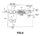
- the third embodiment is an image acquisition circuit which uses a CDS chip 40 in FIG. 8 instead of a CDS chip 4 in FIG. 6 in the first embodiment in FIG. 5.
- This image acquisition circuit also uses the CCD 2 as a solid-state image sensor which converts a subject image to an electric signal.
- An image signal from the CCD 2 is subject to correlated double sampling (CDS).
- CDS correlated double sampling
- GCA Gain applied to the sampled signal
- ADC ADC
- This image acquisition circuit also employs a CCD pixel rate at 30 to 40 MHz in compliance with high-pixel CCDs.
- the CDS chip 40 is provided with the CDS6, the clamp circuit 14, and drivers 9 and 10 same as the CDS chip 4 shown in FIG. 6.
- the third embodiment differs from the first embodiment as follows.
- a single to differential converter 41 is provided at the rear stage of the CDS 6.
- the single to differential converter 41 applies +6 dB gain to the input signal, providing both positive and negative image signals at the output.
- These amplified signals are supplied to drivers 9 and 10.
- the driver 9 sends the sampled signal or the image signal (OUT1) amplified in the single to differential converter 41 to the line 16 via the output terminal 11.
- the driver 10 sends the reversed image signal (OUT2) amplified in the single to differential converter 41 to the line 17 via the output terminal 12.
- the above-mentioned image signal from the CDS 6 is supplied to the clamp circuit 14.
- the clamp circuit 14 clamps the image signal in comparison with the specified DC reference signal and feeds the result back to the CDS 6 input.
- the clamp circuit 14 clamps the image signal (OUT1). Using the clamp circuit 14, as mentioned above, the CDS chip 40 can lower the supply voltage that matches the voltage for the main circuit board.
- the GCA+ADC chip 23 on the main circuit board 20 is supplied with a image signal (OUT 1) from the CCD circuit board 1 via an input terminal 21 connected to the line 16. Concurrently, the GCA+ADC chip 23 is supplied with the reversed image signal (OUT2) from the CCD circuit board 1 via an input terminal 22 connected to the other line 17.
- An internal operation for the GCA+ADC chip 23 is differential, where the negative image signal is subtracted from the positive image signal.
- the drivers 9 and 10 are provided with the same characteristics. If an interfering noise is picked up during transmission, these drivers carry the same contents on the respective transmitted signals. This interfering noise is canceled during the above-mentioned subtraction inside the GCA+ADC chip 23.
- a subtraction output deprived of the interfering noise is equivalent to the image signal.
- the GCA 24 applies gain control to and amplifies the image signal.
- the clamp circuit 25 is installed at an output stage of the GCA 24.
- the clamp circuit 25 clamps an output signal from the GCA 24 and sends the signal to the ADC 26.
- the ADC 26 converts the clamped output signal from the GCA 24 to a digital signal and sends this signal to, say, a DRAM (not shown) as mentioned above.
- the digital signal stored in the DRAM is subject to specified signal processing and is displayed on, say, an LCD monitor. Alternatively, this digital signal is subject to a specified compression and is recorded on tape storage media or the like.
- the third embodiment also uses the same supply voltage of, say, 3 V for the CCD circuit board 1 and the GCA-ADC chip 23. This embodiment eliminates the need for capacitive coupling and enables DC coupling.
Landscapes
- Engineering & Computer Science (AREA)
- Multimedia (AREA)
- Signal Processing (AREA)
- Transforming Light Signals Into Electric Signals (AREA)
Applications Claiming Priority (2)
| Application Number | Priority Date | Filing Date | Title |
|---|---|---|---|
| JP25810599A JP2001086414A (ja) | 1999-09-10 | 1999-09-10 | 撮像装置及び信号処理方法 |
| JP25810599 | 1999-09-10 |
Publications (3)
| Publication Number | Publication Date |
|---|---|
| EP1083741A2 true EP1083741A2 (fr) | 2001-03-14 |
| EP1083741A3 EP1083741A3 (fr) | 2003-01-29 |
| EP1083741B1 EP1083741B1 (fr) | 2008-02-27 |
Family
ID=17315579
Family Applications (1)
| Application Number | Title | Priority Date | Filing Date |
|---|---|---|---|
| EP00307707A Expired - Lifetime EP1083741B1 (fr) | 1999-09-10 | 2000-09-07 | Circuits d'acquisition d'images et de traitement de signal |
Country Status (6)
| Country | Link |
|---|---|
| US (1) | US6801254B1 (fr) |
| EP (1) | EP1083741B1 (fr) |
| JP (1) | JP2001086414A (fr) |
| KR (1) | KR100720304B1 (fr) |
| DE (1) | DE60038146T2 (fr) |
| TW (1) | TW484330B (fr) |
Families Citing this family (16)
| Publication number | Priority date | Publication date | Assignee | Title |
|---|---|---|---|---|
| US7315406B2 (en) * | 2002-06-27 | 2008-01-01 | Transpacific Ip, Ltd. | Scanning circuit structure |
| JP2004328114A (ja) * | 2003-04-22 | 2004-11-18 | Matsushita Electric Ind Co Ltd | アナログ回路及びこれを用いた映像機器 |
| JP4299588B2 (ja) * | 2003-05-29 | 2009-07-22 | 株式会社ルネサステクノロジ | 半導体集積回路装置 |
| JP4566013B2 (ja) * | 2005-01-18 | 2010-10-20 | Hoya株式会社 | 撮像装置 |
| JP4642552B2 (ja) * | 2005-02-03 | 2011-03-02 | Hoya株式会社 | 撮像装置 |
| JP4619981B2 (ja) * | 2006-04-10 | 2011-01-26 | 富士重工業株式会社 | 画像認識装置 |
| JP5111912B2 (ja) * | 2006-05-10 | 2013-01-09 | 株式会社リコー | モータ駆動装置及び画像形成装置 |
| JP4883772B2 (ja) * | 2006-07-13 | 2012-02-22 | キヤノン株式会社 | 画像処理装置及び方法 |
| JP2008236195A (ja) * | 2007-03-19 | 2008-10-02 | Sony Corp | 撮像ブロック及び撮像装置 |
| JP4914482B2 (ja) * | 2009-12-07 | 2012-04-11 | キヤノン株式会社 | 光電変換装置 |
| US8605173B2 (en) | 2010-08-16 | 2013-12-10 | SK Hynix Inc. | Differential column ADC architectures for CMOS image sensor applications |
| CN106303173B (zh) * | 2016-07-19 | 2021-10-15 | 中国科学院西安光学精密机械研究所 | 一种高速低噪声大面阵ccd成像系统及成像方法 |
| KR102324224B1 (ko) | 2017-06-28 | 2021-11-10 | 삼성전자주식회사 | 이미지 센서 및 그것에 포함되는 전자 회로 |
| CN108055527B (zh) * | 2017-12-14 | 2020-06-19 | 南京理工大学 | 通用型emccd测试系统 |
| KR20210112948A (ko) | 2020-03-06 | 2021-09-15 | 삼성전자주식회사 | 상관 이중 샘플링 회로를 포함하는 이미지 센서 |
| US11747555B2 (en) | 2021-10-04 | 2023-09-05 | Eagle Technology, Llc | Optical assembly having commonly-shaped optical modules and associated methods |
Family Cites Families (11)
| Publication number | Priority date | Publication date | Assignee | Title |
|---|---|---|---|---|
| MY108780A (en) * | 1991-09-19 | 1996-11-30 | Sharp Kk | Image sensing apparatus having two image sensing portions and one signal processing portion and allowing improved white balance control. |
| JPH05111048A (ja) * | 1991-10-17 | 1993-04-30 | Sony Corp | ビデオカメラ |
| US5329312A (en) * | 1992-08-17 | 1994-07-12 | Eastman Kodak Company | DC level control circuitry for CCD images |
| JP2994158B2 (ja) * | 1992-11-24 | 1999-12-27 | 株式会社東芝 | 固体撮像装置 |
| US5600696A (en) * | 1995-10-11 | 1997-02-04 | David Sarnoff Research Center, Inc. | Dual-gain floating diffusion output amplifier |
| KR100220863B1 (ko) * | 1995-11-30 | 1999-09-15 | 무네유키 가코우 | 고체촬상소자의 신호독출장치 |
| JP3774499B2 (ja) * | 1996-01-24 | 2006-05-17 | キヤノン株式会社 | 光電変換装置 |
| US5844431A (en) * | 1996-09-18 | 1998-12-01 | Exar Corporation | Low noise low power CMOS correlated double sampler |
| JP3999858B2 (ja) * | 1997-10-03 | 2007-10-31 | オリンパス株式会社 | デジタルカメラの自動露出制御装置 |
| KR100284284B1 (ko) * | 1998-11-05 | 2001-03-02 | 김영환 | 디지털 카메라의 아날로그 신호 처리 장치 |
| US6587143B1 (en) * | 1999-01-19 | 2003-07-01 | National Semiconductor Corporation | Correlated double sampler with single amplifier |
-
1999
- 1999-09-10 JP JP25810599A patent/JP2001086414A/ja active Pending
-
2000
- 2000-09-01 TW TW089117929A patent/TW484330B/zh not_active IP Right Cessation
- 2000-09-05 KR KR1020000052388A patent/KR100720304B1/ko not_active Expired - Fee Related
- 2000-09-07 EP EP00307707A patent/EP1083741B1/fr not_active Expired - Lifetime
- 2000-09-07 DE DE60038146T patent/DE60038146T2/de not_active Expired - Lifetime
- 2000-09-08 US US09/657,900 patent/US6801254B1/en not_active Expired - Fee Related
Also Published As
| Publication number | Publication date |
|---|---|
| EP1083741A3 (fr) | 2003-01-29 |
| JP2001086414A (ja) | 2001-03-30 |
| DE60038146T2 (de) | 2009-06-18 |
| KR20010030269A (ko) | 2001-04-16 |
| TW484330B (en) | 2002-04-21 |
| KR100720304B1 (ko) | 2007-05-22 |
| EP1083741B1 (fr) | 2008-02-27 |
| DE60038146D1 (de) | 2008-04-10 |
| US6801254B1 (en) | 2004-10-05 |
Similar Documents
| Publication | Publication Date | Title |
|---|---|---|
| EP1083741B1 (fr) | Circuits d'acquisition d'images et de traitement de signal | |
| US8553114B2 (en) | Image sensing apparatus and image sensing system | |
| US8421888B2 (en) | Solid state imaging device having signal noise combining circuitry for masking image reproduction errors | |
| US20090066823A1 (en) | Solid-state image pickup device and clamp control method therefor | |
| EP2950524B1 (fr) | Dispositif de capture d'image, système d'endoscope, et procédé de réduction du bruit | |
| CN102893598B (zh) | 阻抗匹配装置和具有该阻抗匹配装置的内窥镜 | |
| EP2094002A2 (fr) | Système de communication d'endoscope et système d'endoscope | |
| JP2008172493A (ja) | フロントエンド信号処理方法およびフロントエンド信号処理装置 | |
| US20090256939A1 (en) | Solid-state imaging apparatus | |
| JP2015119385A (ja) | 撮像装置および撮像システム | |
| US8319850B2 (en) | Imaging element with signal holding section, drive method for imaging element with signal holding period, and camera with imaging element and signal holding section | |
| JPH0329636A (ja) | 電子式内視鏡装置 | |
| US20050088549A1 (en) | Noise removing device for image sensor | |
| US6700608B1 (en) | Image pickup apparatus | |
| CN101868969A (zh) | 摄像设备 | |
| JPH10214956A (ja) | 固体撮像素子 | |
| EP2423962A1 (fr) | Système de capteur d'image numérique à longue exposition | |
| JP3744160B2 (ja) | 映像信号処理方法及び映像信号処理装置 | |
| JP3207229B2 (ja) | 電子内視鏡装置の信号伝送処理回路 | |
| JP4276416B2 (ja) | 画像信号用ゆらぎ補償回路及び電子内視鏡用画像信号処理回路 | |
| JPH114384A (ja) | 固体撮像素子とその駆動方法 | |
| KR100704758B1 (ko) | 씨씨디 카메라 시스템의 화상 신호 보상 장치 | |
| JPH07162761A (ja) | 固体撮像装置 | |
| JPH10262919A (ja) | 電子内視鏡装置 | |
| JPH04258091A (ja) | 固体撮像素子 |
Legal Events
| Date | Code | Title | Description |
|---|---|---|---|
| PUAI | Public reference made under article 153(3) epc to a published international application that has entered the european phase |
Free format text: ORIGINAL CODE: 0009012 |
|
| AK | Designated contracting states |
Kind code of ref document: A2 Designated state(s): AT BE CH CY DE DK ES FI FR GB GR IE IT LI LU MC NL PT SE |
|
| AX | Request for extension of the european patent |
Free format text: AL;LT;LV;MK;RO;SI |
|
| PUAL | Search report despatched |
Free format text: ORIGINAL CODE: 0009013 |
|
| AK | Designated contracting states |
Designated state(s): AT BE CH CY DE DK ES FI FR GB GR IE IT LI LU MC NL PT SE |
|
| AX | Request for extension of the european patent |
Extension state: AL LT LV MK RO SI |
|
| 17P | Request for examination filed |
Effective date: 20030715 |
|
| AKX | Designation fees paid |
Designated state(s): DE FR GB |
|
| 17Q | First examination report despatched |
Effective date: 20061107 |
|
| GRAP | Despatch of communication of intention to grant a patent |
Free format text: ORIGINAL CODE: EPIDOSNIGR1 |
|
| RTI1 | Title (correction) |
Free format text: IMAGE ACQUISITION AND SIGNAL PROCESSING CIRCUITS |
|
| GRAS | Grant fee paid |
Free format text: ORIGINAL CODE: EPIDOSNIGR3 |
|
| GRAA | (expected) grant |
Free format text: ORIGINAL CODE: 0009210 |
|
| AK | Designated contracting states |
Kind code of ref document: B1 Designated state(s): DE FR GB |
|
| REG | Reference to a national code |
Ref country code: GB Ref legal event code: FG4D |
|
| REF | Corresponds to: |
Ref document number: 60038146 Country of ref document: DE Date of ref document: 20080410 Kind code of ref document: P |
|
| ET | Fr: translation filed | ||
| PLBE | No opposition filed within time limit |
Free format text: ORIGINAL CODE: 0009261 |
|
| STAA | Information on the status of an ep patent application or granted ep patent |
Free format text: STATUS: NO OPPOSITION FILED WITHIN TIME LIMIT |
|
| 26N | No opposition filed |
Effective date: 20081128 |
|
| REG | Reference to a national code |
Ref country code: GB Ref legal event code: 746 Effective date: 20120703 |
|
| REG | Reference to a national code |
Ref country code: DE Ref legal event code: R084 Ref document number: 60038146 Country of ref document: DE Effective date: 20120614 |
|
| PGFP | Annual fee paid to national office [announced via postgrant information from national office to epo] |
Ref country code: GB Payment date: 20120920 Year of fee payment: 13 |
|
| GBPC | Gb: european patent ceased through non-payment of renewal fee |
Effective date: 20130907 |
|
| PG25 | Lapsed in a contracting state [announced via postgrant information from national office to epo] |
Ref country code: GB Free format text: LAPSE BECAUSE OF NON-PAYMENT OF DUE FEES Effective date: 20130907 |
|
| PGFP | Annual fee paid to national office [announced via postgrant information from national office to epo] |
Ref country code: DE Payment date: 20140922 Year of fee payment: 15 |
|
| PGFP | Annual fee paid to national office [announced via postgrant information from national office to epo] |
Ref country code: FR Payment date: 20140919 Year of fee payment: 15 |
|
| REG | Reference to a national code |
Ref country code: DE Ref legal event code: R119 Ref document number: 60038146 Country of ref document: DE |
|
| REG | Reference to a national code |
Ref country code: FR Ref legal event code: ST Effective date: 20160531 |
|
| PG25 | Lapsed in a contracting state [announced via postgrant information from national office to epo] |
Ref country code: DE Free format text: LAPSE BECAUSE OF NON-PAYMENT OF DUE FEES Effective date: 20160401 |
|
| PG25 | Lapsed in a contracting state [announced via postgrant information from national office to epo] |
Ref country code: FR Free format text: LAPSE BECAUSE OF NON-PAYMENT OF DUE FEES Effective date: 20150930 |