EP1085355A2 - Circuits optiques fléxibles et fibres optiques incorporés dans de substates poreux et procédés de fabrication - Google Patents
Circuits optiques fléxibles et fibres optiques incorporés dans de substates poreux et procédés de fabrication Download PDFInfo
- Publication number
- EP1085355A2 EP1085355A2 EP00307610A EP00307610A EP1085355A2 EP 1085355 A2 EP1085355 A2 EP 1085355A2 EP 00307610 A EP00307610 A EP 00307610A EP 00307610 A EP00307610 A EP 00307610A EP 1085355 A2 EP1085355 A2 EP 1085355A2
- Authority
- EP
- European Patent Office
- Prior art keywords
- porous substrate
- flexible
- flexible porous
- optical
- encapsulating material
- Prior art date
- Legal status (The legal status is an assumption and is not a legal conclusion. Google has not performed a legal analysis and makes no representation as to the accuracy of the status listed.)
- Granted
Links
Images

Classifications
-
- G—PHYSICS
- G02—OPTICS
- G02B—OPTICAL ELEMENTS, SYSTEMS OR APPARATUS
- G02B6/00—Light guides; Structural details of arrangements comprising light guides and other optical elements, e.g. couplings
- G02B6/24—Coupling light guides
- G02B6/36—Mechanical coupling means
- G02B6/3608—Fibre wiring boards, i.e. where fibres are embedded or attached in a pattern on or to a substrate, e.g. flexible sheets
-
- B—PERFORMING OPERATIONS; TRANSPORTING
- B29—WORKING OF PLASTICS; WORKING OF SUBSTANCES IN A PLASTIC STATE IN GENERAL
- B29D—PRODUCING PARTICULAR ARTICLES FROM PLASTICS OR FROM SUBSTANCES IN A PLASTIC STATE
- B29D11/00—Producing optical elements, e.g. lenses or prisms
- B29D11/0074—Production of other optical elements not provided for in B29D11/00009- B29D11/0073
- B29D11/0075—Connectors for light guides
-
- G—PHYSICS
- G02—OPTICS
- G02B—OPTICAL ELEMENTS, SYSTEMS OR APPARATUS
- G02B6/00—Light guides; Structural details of arrangements comprising light guides and other optical elements, e.g. couplings
- G02B6/24—Coupling light guides
- G02B6/42—Coupling light guides with opto-electronic elements
- G02B6/43—Arrangements comprising a plurality of opto-electronic elements and associated optical interconnections
-
- G—PHYSICS
- G02—OPTICS
- G02B—OPTICAL ELEMENTS, SYSTEMS OR APPARATUS
- G02B6/00—Light guides; Structural details of arrangements comprising light guides and other optical elements, e.g. couplings
- G02B6/44—Mechanical structures for providing tensile strength and external protection for fibres, e.g. optical transmission cables
Definitions
- the present invention relates to optical circuits and, more particularly, to flexible optical circuits having optical fibers encapsulated therein.
- High capacity electronic systems are increasingly adopting optoelectronics as a means to surpass conventional limitations (e.g., transmission speed) of electrical interconnections.
- photonic technology has long been preferred in long-haul communications
- optics is now quickly becoming a viable option for short link applications.
- One demanding short-link application for optical interconnection is in the interboard/shelf or backplane level of communication.
- Most large system equipment today is partitioned into bookshelf levels consisting of multiple printed wiring boards inserted into shelves within a frame or cabinet.
- One interconnect level within such a system is that between two printed circuit boards within the cabinet, known as the backplane level of interconnection.
- Backplane systems are typically organized by mounting various system components on printed wiring boards and interconnecting the printed wiring boards with a circuit transmission element known as a backplane.
- the backplane may include various socket elements for receiving printed wiring boards.
- the circuit density of printed wiring boards increases, it becomes difficult to provide the needed backplane interconnections because, as interconnection transmission lines become thinner, their impedances increase.
- electromagnetic interference between closely adjacent electrical signal parts can reduce signal integrity due to cross-talk and interference.
- the distance over which information must be transmitted by backplane conductors is fairly long compared to the distances transmitted on printed wiring boards. These factors may reduce the speed at which the circuits can be operated, and the signal integrity, which may defeat a principal advantage of higher circuit densities.
- Optical fiber interconnections have been suggested to address these problems.
- optical fiber interconnections are often made of flexible material so that they can be bent for mounting in an appropriate structure to reduce the volume required by the system and to aid in connection to other electronic systems.
- advances in optical fiber interconnections will be discussed with focus on implementation at the backplane level, these interconnections can be utilized in a number of short link applications other than simply those used as backplane connections within a large system cabinet.
- the purpose of the encapsulation is to give the structure mechanical stability, to protect the optical fibers from the surrounding environment, and to keep the optical fibers in place during the handling of the optical backplane.
- the optical fibers of the optical backplane are typically used as large-capacity transmission lines between printed wiring boards or between optical circuits.
- the optical backplane is preferably designed by a computer, which provides optical fiber routes of the appropriate length between input and output ports of the optical backplane.
- a robotic routing machine preferably implements these routes because it is important for optical transmission reliability that there not be undesirable deviations in the prescribed length of each line.
- optical fibers which are usually made of glass, are susceptible to damage, particularly at locations at which the fibers overlap or cross over one another. After the optical fibers have been encapsulated in plastic, strain on an optical fiber at a point of overlap or crossover may be sufficient to break or otherwise diminish performance of the optical fiber. The pressure applied to the plastic sheet which encapsulates the optical fibers may also break the optical fibers, especially at points where the optical fibers overlap or crisscross each other, which is necessary for fiber routing.
- Burack et al. '390 United States Patent No. 5,292,390, to Burack et al. (hereinafter Burack et al. '390), incorporated herein by reference, is assigned to AT&T Bell Laboratories, the predecessor in interest of the assignee of the present invention, and also discloses optical fiber encapsulating techniques for producing optical circuits where a plurality of optical fibers are first bonded to an upper surface of a flat flexible plastic substrate and then are covered with a sheet of thermoplastic material to form a composite structure including the thermoplastic material, the optical fibers and the plastic substrate. This composite structure is then compressed at a first elevated temperature and at a first relatively high pressure which are sufficient to bond or tack the thermoplastic material to the plastic substrate.
- a second elevated temperature is applied to the thermoplastic material while compressing the composite structure at a second pressure.
- the second elevated temperature is higher than the first temperature and is sufficiently high to cause the thermoplastic material to flow about and encase the optical fibers.
- a flexible optical circuit having a plurality of optical fibers is provided by mounting optical fibers to a flexible porous substrate and thereafter encapsulating the optical fibers and porous substrate with a protective encapsulating material.
- the encapsulating material can be a liquid which surrounds the optical fibers and flows through pores in the porous substrate to achieve a structurally sound and protected flexible optical circuit. Because the encapsulating material surrounds and protects the optical fibers, heat and pressure are not required in forming the optical circuit, resulting in reduced optical fiber breakage as compared to prior art methods of constructing flexible optical circuits.
- an optical circuit includes a first flexible porous substrate having an upper surface and a lower surface, an adhesive located on the upper surface of the first flexible porous substrate, and optical fibers attached to the upper surface of the flexible porous substrate by the adhesive.
- the flexible optical circuit also includes an encapsulating material applied to the optical fibers. The encapsulating material completely surrounds the optical fibers and impregnates the first flexible porous substrate to provide strength and protection to the optical circuit.
- the flexible optical circuit may be fabricated by providing a flexible porous substrate with an upper surface and a lower surface, adhering optical fibers to the upper surface of the flexible porous substrate, and applying an encapsulating material to the optical fibers and the flexible porous substrate to provide strength and protection to the optical circuit.
- Adhesive can be applied to the upper surface of the flexible porous substrate to cause the optical fiber to adhere to the upper surface of the flexible porous substrate.
- the flexible porous substrate can comprise a flexible mesh substrate made of kevlar, cotton, plastic, metal, cloth, or other suitable strong and flexible materials.
- the encapsulating material can be applied to the optical circuit by spray-coating the optical fibers and the flexible porous substrate or by dipping the optical circuit into a bath of encapsulating material. Upon curing, the encapsulating material should be flexible and durable.
- a suitable encapsulating material may be, for example, plastic.
- optical fibers are positioned between two porous substrates, and the optical fibers and both of the porous substrates are encapsulated by an encapsulating material.
- the circuit may be fabricated by providing a first flexible porous substrate with an upper surface and a lower surface, applying adhesive to the upper surface of the first flexible porous substrate or to the optical fibers to cause optical fibers to adhere to the upper surface of the first flexible porous substrate, placing the optical fibers on the upper surface of the first flexible porous substrate, placing a second flexible porous substrate on the optical fibers, located opposite the first flexible porous substrate, and applying an encapsulating material to the optical fibers, the first flexible porous substrate, and the second flexible porous substrate to provide strength and protection to the optical circuit.
- an adhesive may be applied to a surface of the second flexible porous substrate that is in contact with the optical fibers to fix the second flexible porous substrate relative to the optical fibers.
- the encapsulating material may be applied to the first and second flexible porous substrates by spray-coating or bath emersion so that the encapsulating material flows through pores in the second flexible porous substrate and pores in the first flexible porous substrate to fill any gaps therebetween, and to substantially surround the optical fibers therebetween.
- the use of porous substrates and encapsulating material provide protection to the optical circuit without the need for lamination or the requirement of pressure. Therefore, optical fiber breakage and optical circuit delamination can be minimized.
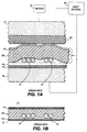
- FIG. 1A shows a cross-sectional view of a conventional flexible optical circuit of the prior art during formation.
- An optical circuit 11 comprises a flexible plastic substrate 12 to which a plurality of optical fibers 13 are adhered by an adhesive layer 14.
- the fibers 13 may be located on the substrate surface by a computer-controlled routing machine, and the adhesive 14 may be a pressure-sensitive adhesive. After the fibers have been routed onto the substrate, it is necessary to encapsulate them to provide structural support for the fibers and to protect them from the environment and from the effects of handling.
- the optical circuit 11 is placed on a lower platen 16 of a press machine which includes an upper platen 17 actuated by a motor 18 .
- a layer 20 of thermoplastic material Over the optical fibers and the plastic substrate is placed a layer 20 of thermoplastic material, and over the layer of thermoplastic material is placed a second substrate 21 of plastic material that is preferably of the same material as plastic substrate 12 .
- a layer 23 of a resilient or spongy thermally conductive material is located between the upper plastic substrate 21 and the upper platen 17 .
- the purpose of the layer 23 is to transmit heat from platen 17 and to distribute stresses over the optical backplane structure so as to avoid concentrations of stress that might damage optical fibers.
- the composite structure comprising plastic substrates 12 and 21 , thermoplastic layer 20 and optical fibers 13 is then heated by a heat source 25 to bond the two plastic substrates 12 and 21 .
- FIG. 1B shows the conventional flexible optical circuit 11 of FIG. 1A after formation is complete.
- the optical fibers 13 are encapsulated within the flexible plastic substrates 12 , 21 without suffering damage as the plastic substrates 12 , 21 are securely laminated together.
- this conventional technique as described in U.S. Patent No. 5,292,390 to Burack et al., may result in some negative consequences.
- the optical fibers 13 may break, or coating of the optical fibers 13 may be damaged, usually at cross-over points, thereby degrading optical circuit performance.
- the optical fibers 13 being constructed of glass or plastic which cannot withstand the pressure and heat of lamination, particularly at locations where the optical fibers cross-over. Furthermore, the lamination process may result in trapped air located between the first plastic substrate 12 and second plastic substrate 21 . The trapped air can expand and shrink, causing the lamination to fail, resulting in plastic layer separation, especially when the optical circuit 11 is placed in an environment having extremely low or high temperatures or large temperature fluctuations. The separation of the plastic substrates 12 , 21 can result in free movement of the optical fibers 13 , increasing the likelihood of optical fiber 13 breakage, or displacement of the optical fibers 13 at a portion of the optical circuit 11 where connections to the optical fibers 13 are made. These consequences, as will be appreciated by those of skill in the art, can result in poor performance of the optical circuit 11 .
- the present invention overcomes many of the negative aspects of prior art flexible optical circuits by mounting optical fibers to a flexible porous substrate and thereafter encapsulating the optical fibers and porous substrate with a protective encapsulating material.
- the encapsulating material can be a liquid which surrounds the optical fibers and flows through pores in the porous substrate to achieve a structurally sound and protected flexible optical circuit.
- optical fibers may be positioned between two porous substrates, where the fibers and both the porous substrates are encapsulated by an encapsulating material.
- the encapsulating material functions to surround and protect the optical fibers, and obviates the need for heat and pressure in forming the optical circuit, resulting in reduced optical fiber damage and breakage as compared to prior art methods of constructing flexible optical circuits.
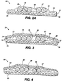
- FIG. 2A shows a cross-sectional view of a flexible optical circuit in accordance with an embodiment of the invention.
- the flexible optical circuit 30 comprises a flexible porous substrate 35 , having a lower surface 36 and an upper surface 37 .
- a function of the flexible porous substrate 35 is to act as a base structure upon which the remainder of the optical circuit 30 may be formed.
- the flexible porous substrate 35 is shown to be a flexible mesh.
- the mesh may comprise material made of cloth, kevlar (such as KEVLAR, a registered trademark of E. I. du Pont de Nemours and Company), plastic, cotton, metal, or any other suitable flexible porous material which may support other elements, as described below, of the optical circuit 30 .
- the adhesive 40 is applied to the upper surface 37 of the flexible porous substrate 35 .
- the adhesive 40 is preferably a relatively strong adhesive, which provides tackiness to cause a lower portion 46 of at least one of a plurality of optical fibers 45 to adhere to the upper surface 37 of the flexible porous substrate 35 .
- the optical fibers 45 should adhere to the flexible porous substrate 35 so that the optical fibers 45 do not move during or subsequent to the formation of the optical circuit 30 . If the optical fibers 45 move during formation of the optical circuit 30, then the optical fibers 45 may be out of place at an end portion (not shown) of the optical circuit 30 where the optical fibers 45 should be precisely aligned for connection to external components.
- the adhesive 40 may be applied using conventional techniques well known in the art. As is illustrated in FIG. 2B, the adhesive 40 is preferably applied to the flexible porous substrate 35 in a manner which does not fill in pores 38 of the flexible porous substrate 35 . In FIG. 2B, the flexible porous substrate 35 is a flexible mesh illustrated with phantom lines, due to the upper surface of the mesh being covered with adhesive 40 . Although FIG. 2B shows the mesh to comprise extremely thin filaments, it will be appreciated by those of skill in the art that the types and sizes of mesh or porous substrates 35 that may be utilized may vary. The adhesive 40 coats only each individual filament of the mesh, rather than the mesh in its entirety.
- the mesh remains porous, although the area of the pores 38 may be diminished due to coating of the material which makes up the porous mesh.
- the adhesive 40 may be applied directly to the optical fibers 45 as the optical fibers 45 are being deposited on the porous substrate 35.
- the adhesive 40 may be a conventional adhesive, such as a silicone adhesive, an acrylic adhesive, a rubber based adhesive, a pressure sensitive adhesive, combinations thereof, or other suitable adhesives well known to those of skill in the art. Additionally, the adhesive can be flame retardant, so as not to act as a fuse if one end of the optical circuit 30 catches on fire.
- the optical fibers 45 adhered to the upper surface 37 of the flexible porous substrate 35 can include a number of different optical fiber types, although a conventional dual acrylic coated glass fiber having a total outside diameter of either two hundred fifty or one hundred twenty five microns is preferred.
- the optical fibers 45 may be placed on the upper surface 37 of the flexible porous substrate 35 by a human operator, the optical fibers 45 are preferably placed onto the flexible porous substrate 35 by a mechanical routing machine.
- a mechanical routing machine is disclosed in U.S. Patent No. 5,259,051, to Burack et al. Such a routing machine enables optical circuits 30 to be mass produced and can reduce the operator skill required for optical circuit fabrication.
- the routing machine can accurately align optical fibers 45 of the optical circuit 30 so that a precise length of an optical fiber is used for a given path, which may be important in some high speed digital systems where deviations in optical fiber length can result in timing and synchronization errors. It should be realized, however, that any such machine must be able to route optical fibers 45 that are relatively fragile and less flexible than conventional electrical conductors, such as electrical wire. Because the flexible porous substrate 35 is flexible, the substrate 35 may either be temporarily mounted on a carrier board (e.g., by a light adhesive or other securing means), or may be stretched so as to be taut, thereby allowing optical fiber 45 placement thereon.
- an encapsulating material 49 is applied to the optical fibers 45 and the flexible porous substrate to provide strength and protection to the optical circuit 30 .
- the encapsulating material 49 can completely surround the optical fibers 45 , including an upper portion 47 of the optical fibers 45 , as well as the flexible porous substrate 35 , as shown in FIG. 2A (note that the encapsulating material 49 is not illustrated in FIG. 2B). Because the flexible porous substrate 35 contains pores 38 , the encapsulating material 49 may impregnate the flexible porous substrate 35 . After application, the encapsulating material may then cure.
- the function of the encapsulating material 49 is to ensure that no unfilled gaps exist between adjacent optical fibers 45 , or between the optical fibers 45 and the flexible porous substrate 35 , and to strengthen the flexible porous substrate 35 and to bond the flexible porous substrate 35 and the optical fibers 45 .
- the encapsulating material 49 of the present invention conforms to the shapes of the optical fibers 45 .
- the encapsulating material 49 may be in a liquid form so that the encapsulating material 49 can fill any gaps.
- the encapsulating material 49 can be silicone, silicone rubber, polyvinyl chloride (pvc), polyurethane, epoxy, or another suitable material known to those of skill in the art which is flexible, is durable, is inexpensive, can encapsulate the optical fibers 45 and flexible porous substrate 35 , protects the circuit from external environments, and provides sufficient structural rigidity.
- the encapsulating material 49 should be of proper viscosity so that when applied to the optical fibers 45 and flexible porous substrate 35 , the encapsulating material 49 penetrates the pores 38 and adhere to the optical fibers 45 and flexible porous substrate 35 .
- the flexible porous substrate 35 should have adequate coarseness on at least one portion, such as the lower surface 36 , so as to allow the encapsulating material 49 to adhere to the substrate 35 .
- the encapsulating material 49 may be applied utilizing a number of techniques.
- the encapsulating material 49 can be sprayed onto the optical fibers using conventional spray-coating techniques.
- the optical circuit 30 can be dipped into a bath of the encapsulating material 49 . If the optical circuit 30 is dipped into encapsulating material 49 , the optical circuit 30 may undergo a step, such as hanging, to allow excess encapsulating material to be removed.
- FIG. 3 shows a cross-sectional view of a flexible optical circuit 70 in accordance with a second embodiment of the invention.
- the flexible optical circuit 70 comprises a first flexible porous substrate 55 , having a lower surface 56 and an upper surface 57 , an adhesive 60 applied to the upper surface 57 of the first flexible porous substrate 55 , and optical fibers 65 fixed to the first flexible porous substrate 55 at a lower portion 66.
- a second flexible porous substrate 72 which covers an upper portion 67 of the optical fibers 65.
- the second flexible porous substrate 72 After the optical fibers 65 are adhered to the upper surface 57 of the first flexible porous substrate 55 , but prior to the application of an encapsulating material 79 , the second flexible porous substrate 72 , having a lower surface 76 and an upper surface 77 , is placed over the optical fibers 65 so as to sandwich the optical fibers 65 between the first and second flexible porous substrates 55 , 72 .
- the second flexible porous substrate 72 functions to provide additional support to the optical circuit 70 , and may be constructed of similar materials used to construct the first flexible porous substrate 55 , including the same material.
- both the first flexible porous substrate 55 and the second flexible porous substrate 72 are shown to be flexible mesh, which may comprise mesh cloth, kevlar, plastic, cotton, metal, or any other flexible porous material providing support to the optical circuit 70 .
- an encapsulating material 79 is applied to the optical circuit 70.
- the encapsulating material 79 can be sprayed onto the optical fibers using conventional spray-coating techniques, or the optical circuit 70 can be dipped into the encapsulating material 79 . If the encapsulating material 79 is spray-coated, it is preferred that the encapsulating material 79 be of proper viscosity so that it penetrates the pores in the first and second flexible porous substrates 55 , 72 to fill any gaps located between the first flexible porous substrate 55 and the second flexible porous substrate 72 .
- the optical circuit 70 may be flipped over for application of encapsulating material 79 onto the first flexible porous substrate 55 during the spray-coating process to ensure proper saturation of encapsulating material through pores in both the first flexible porous substrate 55 and pores in the second flexible porous substrate 72 .
- the use of the second flexible porous substrate 72 provides the optical circuit 70 with additional strength over the optical circuit 30 embodied in FIG. 2A, although the additional materials will most likely result in relatively higher costs.
- no pressure is applied to the optical fibers during construction of the optical circuit 70 .
- the present invention can provide a strong, flexible optical circuit 70 with less likelihood of optical fiber damage than prior art techniques.
- expensive lamination processes are not required for the optical circuit 70 construction.
- FIG. 4 a cross-sectional view of a flexible optical circuit 88 in accordance with a third embodiment of the invention.
- the optical circuit 88 of the embodiment shown in FIG. 4 is substantially identical in structure and construction to the optical circuit 70 embodiment of FIG. 4 except for the addition of an adhesive layer 87 located between the second flexible porous substrate 82 and the optical fibers 85 .
- This adhesive layer can be applied to the second flexible porous substrate 82 prior to the placement of the substrate 82 on the optical fibers 85 , in the same manner the adhesive 40 is applied to the flexible porous substrate 35 , as described above with respect to FIG.
- the function of the adhesive 87 is to fix the optical fibers 85 in place with respect to the second flexible porous substrate 82 prior to the addition of encapsulating material 90 , which secures optical circuit 88 elements relative to one another.
- the adhesive layer 87 should leave pores open so that the encapsulating material 90 can penetrate the porous substrates 82 , 83 to fill gaps in the optical circuit 88 .
- this embodiment produces a strong optical circuit 88 without the use of heat and pressure during formation of the optical circuit 88 , resulting in reduced optical fiber 85 breakage as compared to prior art methods of constructing optical circuits.
Landscapes
- Physics & Mathematics (AREA)
- General Physics & Mathematics (AREA)
- Optics & Photonics (AREA)
- Engineering & Computer Science (AREA)
- Health & Medical Sciences (AREA)
- Manufacturing & Machinery (AREA)
- Ophthalmology & Optometry (AREA)
- Mechanical Engineering (AREA)
- Light Guides In General And Applications Therefor (AREA)
Applications Claiming Priority (2)
| Application Number | Priority Date | Filing Date | Title |
|---|---|---|---|
| US397307 | 1999-09-16 | ||
| US09/397,307 US6370293B1 (en) | 1999-09-16 | 1999-09-16 | Flexible optical circuits having optical fibers encapsulated between porous substrates and methods for fabricating same |
Publications (3)
| Publication Number | Publication Date |
|---|---|
| EP1085355A2 true EP1085355A2 (fr) | 2001-03-21 |
| EP1085355A3 EP1085355A3 (fr) | 2004-01-28 |
| EP1085355B1 EP1085355B1 (fr) | 2010-11-03 |
Family
ID=23570681
Family Applications (1)
| Application Number | Title | Priority Date | Filing Date |
|---|---|---|---|
| EP00307610A Expired - Lifetime EP1085355B1 (fr) | 1999-09-16 | 2000-09-04 | Procédé de fabrication de circuits optiques flexibles ayant des fibres optiques incorporées dans des substrats poreux |
Country Status (4)
| Country | Link |
|---|---|
| US (1) | US6370293B1 (fr) |
| EP (1) | EP1085355B1 (fr) |
| JP (1) | JP3844644B2 (fr) |
| DE (1) | DE60045179D1 (fr) |
Cited By (2)
| Publication number | Priority date | Publication date | Assignee | Title |
|---|---|---|---|---|
| US7275562B2 (en) | 2001-10-17 | 2007-10-02 | Agilent Technologies, Inc. | Extensible spiral for flex circuit |
| US9017509B2 (en) | 2010-03-02 | 2015-04-28 | Bae Systems Plc | Optical fibre fixed on substrates |
Families Citing this family (6)
| Publication number | Priority date | Publication date | Assignee | Title |
|---|---|---|---|---|
| US6690867B2 (en) * | 2001-08-31 | 2004-02-10 | Corning Cable Systems Llc | Optical interconnect assemblies and methods therefor |
| US6636685B2 (en) * | 2002-01-30 | 2003-10-21 | Fitel Usa Corp. | Systems and methods for fabricating flexible optical fiber circuits |
| US7233712B2 (en) * | 2002-04-22 | 2007-06-19 | Sanmina-Sci Corporation | Temperature-controlled flexible optical circuit for use in an erbium-doped fiber amplifier and method for fabricating the flexible optical circuit |
| US7015075B2 (en) * | 2004-02-09 | 2006-03-21 | Freescale Semiconuctor, Inc. | Die encapsulation using a porous carrier |
| JP2008191409A (ja) * | 2007-02-05 | 2008-08-21 | Fujikura Ltd | 光ファイバシート |
| US12196951B2 (en) * | 2021-03-09 | 2025-01-14 | The Government Of The United States Of America, As Represented By The Secretary Of The Navy | Optomechanical fiber actuator |
Family Cites Families (8)
| Publication number | Priority date | Publication date | Assignee | Title |
|---|---|---|---|---|
| DE3020622C2 (de) * | 1980-05-30 | 1985-05-15 | W.L. Gore & Associates, Inc., Newark, Del. | Bandkabel und Verfahren zu seiner Herstellung |
| US5155785A (en) | 1991-05-01 | 1992-10-13 | At&T Bell Laboratories | Optical fiber interconnection apparatus and method |
| US5276759A (en) * | 1992-01-09 | 1994-01-04 | Raychem Corporation | Flat cable |
| US5259051A (en) | 1992-08-28 | 1993-11-02 | At&T Bell Laboratories | Optical fiber interconnection apparatus and methods of making interconnections |
| US5292390A (en) | 1992-09-30 | 1994-03-08 | At&T Bell Laboratories | Optical fiber encapsulating techniques |
| US5394504A (en) | 1994-02-24 | 1995-02-28 | At&T Corp. | Optical fiber encapsulation techniques |
| DE19626514B4 (de) * | 1996-07-02 | 2007-01-18 | W.L. Gore & Associates Gmbh | Optische Vorrichtung mit zusammendrückbarem Laminat |
| US5981064A (en) * | 1997-11-20 | 1999-11-09 | Lucent Technologies Inc. | Flexible filament device with pressure-sensitive flame retardant adhesive |
-
1999
- 1999-09-16 US US09/397,307 patent/US6370293B1/en not_active Expired - Lifetime
-
2000
- 2000-09-04 DE DE60045179T patent/DE60045179D1/de not_active Expired - Lifetime
- 2000-09-04 EP EP00307610A patent/EP1085355B1/fr not_active Expired - Lifetime
- 2000-09-14 JP JP2000279017A patent/JP3844644B2/ja not_active Expired - Fee Related
Cited By (2)
| Publication number | Priority date | Publication date | Assignee | Title |
|---|---|---|---|---|
| US7275562B2 (en) | 2001-10-17 | 2007-10-02 | Agilent Technologies, Inc. | Extensible spiral for flex circuit |
| US9017509B2 (en) | 2010-03-02 | 2015-04-28 | Bae Systems Plc | Optical fibre fixed on substrates |
Also Published As
| Publication number | Publication date |
|---|---|
| EP1085355B1 (fr) | 2010-11-03 |
| DE60045179D1 (de) | 2010-12-16 |
| US6370293B1 (en) | 2002-04-09 |
| JP3844644B2 (ja) | 2006-11-15 |
| EP1085355A3 (fr) | 2004-01-28 |
| JP2001116930A (ja) | 2001-04-27 |
Similar Documents
| Publication | Publication Date | Title |
|---|---|---|
| US6850671B2 (en) | Optical circuit having legs in a stacked configuration and an associated fabrication method | |
| US5292390A (en) | Optical fiber encapsulating techniques | |
| US6005991A (en) | Printed circuit board assembly having a flexible optical circuit and associated fabrication method | |
| CN1231777C (zh) | 光学互连设备及其制造方法 | |
| CN100507624C (zh) | 高密度光纤背板及其制造方法和包括光纤背板的光纤网络装置 | |
| CN1571934B (zh) | 交叉连接光纤的方法和设备 | |
| EP1102095B1 (fr) | Procédé de fabrication des appareils optiques d'interconnexion et appareil optique d'interconnexion | |
| US6567603B1 (en) | Optical interconnection apparatus and process for fabrication of the same | |
| US6370293B1 (en) | Flexible optical circuits having optical fibers encapsulated between porous substrates and methods for fabricating same | |
| CN103814318A (zh) | 柔性光学线路 | |
| US6416232B1 (en) | Device for optical connection | |
| US8891912B2 (en) | Optical ribbon and method of forming same | |
| EP1361464B1 (fr) | Dispositif d'interconnexion optique | |
| KR100386551B1 (ko) | 광섬유 플렉스포일의 적층 | |
| JP3513372B2 (ja) | 光配線板 | |
| CN110187458A (zh) | 光纤线路板及其制造方法、光传输装置及混合光纤线路板 | |
| US6272263B1 (en) | Fibre optic routing system | |
| CN118254394A (zh) | 连续纤维增强复合材料内嵌集束光纤及垂直引出方法 | |
| JP3609942B2 (ja) | 光学接続部品およびその作製方法 | |
| CN217546396U (zh) | 光电混合电路板以及电子装置 | |
| JP3326402B2 (ja) | 光学接続部品 | |
| JPS63161413A (ja) | 回路基板および回路基板の製造方法 | |
| JP2000121879A (ja) | 光学接続部品およびその作製方法 | |
| CN113721329A (zh) | 一种柔性板封装的光模块及其封装方法 |
Legal Events
| Date | Code | Title | Description |
|---|---|---|---|
| PUAI | Public reference made under article 153(3) epc to a published international application that has entered the european phase |
Free format text: ORIGINAL CODE: 0009012 |
|
| AK | Designated contracting states |
Kind code of ref document: A2 Designated state(s): AT BE CH CY DE DK ES FI FR GB GR IE IT LI LU MC NL PT SE |
|
| AX | Request for extension of the european patent |
Free format text: AL;LT;LV;MK;RO;SI |
|
| PUAL | Search report despatched |
Free format text: ORIGINAL CODE: 0009013 |
|
| AK | Designated contracting states |
Kind code of ref document: A3 Designated state(s): AT BE CH CY DE DK ES FI FR GB GR IE IT LI LU MC NL PT SE |
|
| AX | Request for extension of the european patent |
Extension state: AL LT LV MK RO SI |
|
| RIC1 | Information provided on ipc code assigned before grant |
Ipc: 7G 02B 6/44 B Ipc: 7G 02B 6/36 A |
|
| 17P | Request for examination filed |
Effective date: 20040405 |
|
| 17Q | First examination report despatched |
Effective date: 20040721 |
|
| AKX | Designation fees paid |
Designated state(s): DE FR GB |
|
| RAP3 | Party data changed (applicant data changed or rights of an application transferred) |
Owner name: LUCENT TECHNOLOGIES INC. |
|
| RTI1 | Title (correction) |
Free format text: METHOD FOR FABRICATING A FLEXIBLE OPTICAL CIRCUIT HAVING OPTICAL FIBERS ENCAPSULATED BETWEEN POROUS SUBSTRATES |
|
| GRAP | Despatch of communication of intention to grant a patent |
Free format text: ORIGINAL CODE: EPIDOSNIGR1 |
|
| GRAS | Grant fee paid |
Free format text: ORIGINAL CODE: EPIDOSNIGR3 |
|
| GRAA | (expected) grant |
Free format text: ORIGINAL CODE: 0009210 |
|
| AK | Designated contracting states |
Kind code of ref document: B1 Designated state(s): DE FR GB |
|
| REG | Reference to a national code |
Ref country code: GB Ref legal event code: FG4D |
|
| REF | Corresponds to: |
Ref document number: 60045179 Country of ref document: DE Date of ref document: 20101216 Kind code of ref document: P |
|
| PLBE | No opposition filed within time limit |
Free format text: ORIGINAL CODE: 0009261 |
|
| STAA | Information on the status of an ep patent application or granted ep patent |
Free format text: STATUS: NO OPPOSITION FILED WITHIN TIME LIMIT |
|
| 26N | No opposition filed |
Effective date: 20110804 |
|
| REG | Reference to a national code |
Ref country code: DE Ref legal event code: R097 Ref document number: 60045179 Country of ref document: DE Effective date: 20110804 |
|
| PGFP | Annual fee paid to national office [announced via postgrant information from national office to epo] |
Ref country code: DE Payment date: 20130927 Year of fee payment: 14 |
|
| PGFP | Annual fee paid to national office [announced via postgrant information from national office to epo] |
Ref country code: GB Payment date: 20141127 Year of fee payment: 15 Ref country code: FR Payment date: 20141118 Year of fee payment: 15 |
|
| REG | Reference to a national code |
Ref country code: DE Ref legal event code: R119 Ref document number: 60045179 Country of ref document: DE |
|
| REG | Reference to a national code |
Ref country code: DE Ref legal event code: R119 Ref document number: 60045179 Country of ref document: DE Effective date: 20150401 |
|
| PG25 | Lapsed in a contracting state [announced via postgrant information from national office to epo] |
Ref country code: DE Free format text: LAPSE BECAUSE OF NON-PAYMENT OF DUE FEES Effective date: 20150401 |
|
| GBPC | Gb: european patent ceased through non-payment of renewal fee |
Effective date: 20150904 |
|
| REG | Reference to a national code |
Ref country code: FR Ref legal event code: ST Effective date: 20160531 |
|
| PG25 | Lapsed in a contracting state [announced via postgrant information from national office to epo] |
Ref country code: GB Free format text: LAPSE BECAUSE OF NON-PAYMENT OF DUE FEES Effective date: 20150904 |
|
| PG25 | Lapsed in a contracting state [announced via postgrant information from national office to epo] |
Ref country code: FR Free format text: LAPSE BECAUSE OF NON-PAYMENT OF DUE FEES Effective date: 20150930 |