EP1085666A2 - Funksendeempfänger - Google Patents
Funksendeempfänger Download PDFInfo
- Publication number
- EP1085666A2 EP1085666A2 EP00119474A EP00119474A EP1085666A2 EP 1085666 A2 EP1085666 A2 EP 1085666A2 EP 00119474 A EP00119474 A EP 00119474A EP 00119474 A EP00119474 A EP 00119474A EP 1085666 A2 EP1085666 A2 EP 1085666A2
- Authority
- EP
- European Patent Office
- Prior art keywords
- substrate
- receiver
- circuit
- transmitter
- signal
- Prior art date
- Legal status (The legal status is an assumption and is not a legal conclusion. Google has not performed a legal analysis and makes no representation as to the accuracy of the status listed.)
- Ceased
Links
- 239000000758 substrate Substances 0.000 claims abstract description 111
- 230000005540 biological transmission Effects 0.000 claims abstract description 37
- 230000008054 signal transmission Effects 0.000 claims description 32
- 238000006243 chemical reaction Methods 0.000 description 10
- 238000012546 transfer Methods 0.000 description 3
- 238000004891 communication Methods 0.000 description 2
- 239000000470 constituent Substances 0.000 description 2
- 238000007796 conventional method Methods 0.000 description 2
- 238000002955 isolation Methods 0.000 description 2
- 238000012986 modification Methods 0.000 description 2
- 230000004048 modification Effects 0.000 description 2
- RYGMFSIKBFXOCR-UHFFFAOYSA-N Copper Chemical compound [Cu] RYGMFSIKBFXOCR-UHFFFAOYSA-N 0.000 description 1
- 238000010420 art technique Methods 0.000 description 1
- 229910052802 copper Inorganic materials 0.000 description 1
- 239000010949 copper Substances 0.000 description 1
- 238000013461 design Methods 0.000 description 1
- 238000012545 processing Methods 0.000 description 1
Images


Classifications
-
- H—ELECTRICITY
- H05—ELECTRIC TECHNIQUES NOT OTHERWISE PROVIDED FOR
- H05K—PRINTED CIRCUITS; CASINGS OR CONSTRUCTIONAL DETAILS OF ELECTRIC APPARATUS; MANUFACTURE OF ASSEMBLAGES OF ELECTRICAL COMPONENTS
- H05K1/00—Printed circuits
- H05K1/02—Details
- H05K1/0213—Electrical arrangements not otherwise provided for
- H05K1/0216—Reduction of cross-talk, noise or electromagnetic interference
- H05K1/0218—Reduction of cross-talk, noise or electromagnetic interference by printed shielding conductors, ground planes or power plane
-
- H—ELECTRICITY
- H04—ELECTRIC COMMUNICATION TECHNIQUE
- H04B—TRANSMISSION
- H04B1/00—Details of transmission systems, not covered by a single one of groups H04B3/00 - H04B13/00; Details of transmission systems not characterised by the medium used for transmission
- H04B1/38—Transceivers, i.e. devices in which transmitter and receiver form a structural unit and in which at least one part is used for functions of transmitting and receiving
- H04B1/40—Circuits
- H04B1/403—Circuits using the same oscillator for generating both the transmitter frequency and the receiver local oscillator frequency
Definitions
- the present invention is related to an improved receiver/transmitter apparatus by making use of frequencies of microwaves, millimeter waves or the like.
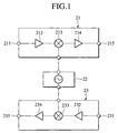
- the reference 21 designates a transmitter circuit whose input terminal 211 is provided for receiving a transmission signal.
- the transmission signal as received is amplified by an amplifier 212 and is inputted to a mixer 213.
- the transmission signal is mixed with a local oscillating signal supplied from a local oscillator 22 and given the frequency conversion into a high transmission frequency.
- the transmission signal is amplified by an amplifier 214 and outputted through an ouput terminal 215.
- a received signal is input through an input terminal 231 of the receiver circuit 23, amplified by an amplifier 232 and transmitted to a mixer 233.
- the received signal is mixed with the local oscillating signal as supplied from the local oscillator 22 and subjected to frequency conversion processing into a lower reception frequency.
- the transmission signal after the frequency conversion is amplified by an amplifier 234 in order to output through an ouput terminal 235.
- the receiver/transmitter apparatus in accordance with the conventional technique is implemented with separate cases for accommodating the transmitter circuit, the receiver circuit and the local oscillator respectively while the respective circuits are connected to each other by means of the respective cases, cables, connectors and so forth. For this reason, the entire volume of the receiver/transmitter apparatus tends to increase. Furthermore, since the respective cases are connected by means of cables and the like, the power loss tends to increase. As a result, it becomes difficult to put the receiver/transmitter apparatus into massproduction and cut down the price.
- the present invention has been made in order to solve the shortcomings as described above. It is an object of the present invention to provide a receiver/transmitter apparatus which can be manufactured in massproduction at a low cost.
- an electric power source circuit for supplying a bias voltage to the transmitter circuit, the local oscillator and the receiver circuit is formed on said substrate between said transmitter circuit and said receiver circuit.
- further improvement resides in that substrate has a principal surface on which a ground electrode is formed.
- further improvement resides in that said through hall sequence is formed along a signal transmission line through which the transmission signal and the received signal are transferred through signal transmission line between the ground electrode formed on the surface of said substrate and the ground electrode formed on the rear surface of said substrate.
- said substrate is composed of a plurality of sublayers each of which has a principal surface on which a ground electrode is formed and a rear surface on which a ground electrode is formed, and wherein a signal transmission line is provided in each sublayer for transferring the transmission signal and/or the received signal.
- a new and improved receiver/transmitter apparatus comprising:
- further improvement resides in that said through hall sequences are arranged in order to form a third substrate region as well as said first and second substrate regions, and wherein said local oscillator, said transmitter circuit and said receiver circuit are located in said first and second substrate regions respectively and isolated from each other by means of said first and second substrate regions.
- an electric power source circuit for supplying a bias voltage to the transmitter circuit, the local oscillator and the receiver circuit is formed on said substrate between said transmitter circuit and said receiver circuit.
- said through hall sequence is formed along a signal transmission line through which the transmission signal or the received signal are transmitted.
- said through hall sequence is extending to reach to the vicinity of one edge of said substrate.
- said through hall sequence is extending to reach to the vicinities of the opposite edges of said substrate.
- further improvement resides in that substrate has a principal surface on which a ground electrode is formed.
- further improvement resides in that said through hall sequence is formed along a signal transmission line through which the transmission signal and the received signal are transferred through signal transmission line between the ground electrode formed on the surface of said substrate and the ground electrode formed on the rear surface of said substrate.
- said substrate is composed of a plurality of sublayers each of which has a principal surface on which a ground electrode is formed and a rear surface on which a ground electrode is formed, and wherein a signal transmission line is provided in each sublayer for transferring the transmission signal and/or the received signal.
- a new and improved receiver/transmitter apparatus comprising:
- further improvement resides in that substrate has a principal surface on which a ground electrode is formed.
- further improvement resides in that said through hall sequence is formed along a signal transmission line through which the transmission signal and the received signal are transferred through signal transmission line between the ground electrode formed on the surface of said substrate and the ground electrode formed on the rear surface of said substrate.
- said substrate is composed of a plurality of sublayers each of which has a principal surface on which a ground electrode is formed and a rear surface on which a ground electrode is formed, and wherein a signal transmission line is provided in each sublayer for transferring the transmission signal and/or the received signal.
- an electric power source circuit for supplying a bias voltage to the transmitter circuit, the local oscillator and the receiver circuit is formed on said substrate between said transmitter circuit and said receiver circuit.
- the present invention is related to a receiver/transmitter apparatus which is driven at very high frequencies which are no lower than 10 GHz such as the KU band, i.e., 12 to 14 GHz for use in BS converters or CS converters, 20 to 40 GHz for use in PTMP (Point-to-MultiPoint) communication systems and so forth.
- the embodiments of the present invention as explained in the followings are directed to receiver/transmitter apparatuses to be implemented within a PTMP communication system.
- Fig.2 is a schematic plan view showing the structure of the embodiment.
- the reference 10 designates a circuit board structure.
- the circuit board structure is composed of a multilayer substrate 11 is implemented with necessary circuitry for realizing the operation of the receiver/transmitter device.
- the substrate 11 is segmented in three regions, i.e., regions A and B located in the upper and lower positions in the figure and a region C located in the center and, for example, is mounted upon a casing (not shown in the figure).
- the transmitter circuit 12 is composed of an input terminal 121, an amplifier 122, a mixer 123, an amplifier 124, an output terminal 125, signal transmission lines 126 for making connection thereamong and so forth.
- the receiver circuit 13 is composed of an input terminal 131, an amplifier 132, a mixer 133, an amplifier 134, an output terminal 135, signal transmission lines 136 for making connection thereamong and so forth.
- a local oscillator 14 for generating a local oscillating signal and an electric power source circuit 15 are located in the region C of the substrate 11 between the region A and the region B.
- a signal transmission line 141a is located in order to connect the local oscillator 14 and the mixer 123 of the transmitter circuit 12 while a signal transmission line 141b serves to connect the local oscillator 14 and the mixer 133 of the receiver circuit 13.
- a bias voltage is supplied from the electric power source circuit 15 to the amplifier 122, the mixer 123 and the amplifier 124 constituting the transmitter circuit 12 and the amplifier 132, the mixer 133 and the amplifier 134 constituting the receiver circuit 13.
- a transmission signal is input to the transmitter circuit 12 through the input terminal 121 and is amplified by the amplifier 122. Thereafter, the transmission signal is input to the mixer 123 and is mixed with the local oscillating signal as supplied from the local oscillator 14 in order to be transmitted at a higher transmission frequency.
- the transmission signal after the frequency conversion is amplified by the amplifier 124 and outputted through the ouput terminal 125.
- the received signal is input from the input terminal 131 to the receiver circuit 13, amplified by the amplifier 132 and input to the mixer 133.
- the received signal is mixed with the local oscillating signal as generated by the local oscillator 14 and subjected to the frequency conversion in order to receive at a lower reception frequency.
- the received signal after the frequency conversion is outputted through the ouput terminal 135.
- the transmitter circuit 12 is located in one side of the substrate 11; the receiver circuit 13 is located in the opposite side of the substrate 11; and the local oscillator 14 and the electric power source circuit 15 are located in the center position therebetween.
- the local oscillator 14 and the electric power source circuit 15 are located between the transmitter circuit 12 and the receiver circuit 13, there is formed effective isolation configuration between the transmitter circuit 12 and the receiver circuit 13.
- the receiver/transmitter apparatus consisting of the transmitter circuit 12, the receiver circuit 13, the local oscillator 14 and the electric power source circuit 15 are formed on the common substrate 11. Because of this, the receiver/transmitter apparatus can be manufactured in a compact design with a reduced number of constituent parts.
- the receiver/transmitter apparatus can formed on a common substrate having rear surface on which a ground electrode is formed. However, the receiver/transmitter apparatus can be formed on a substrate on whose opposite surfaces ground electrodes are formed. Also, in this case, the transmitter circuit is located in one side of the substrate; the receiver circuit is located in the opposite side of the substrate; and the local oscillator and the electric power source circuit are located in the center position.
- both the local oscillator and the electric power source circuit are located in the region between the transmitter circuit and the receiver circuit.
- the local oscillator and the electric power source circuit are located between the transmitter circuit and the receiver circuit. For this reason, even in the case that there is a substantial differential level between the transmission electric power and the reception electric power, it is possible to sufficiently isolate the transmitter circuit and the receiver circuit from each other. Furthermore, it is possible to realize the receiver/transmitter apparatus which posseses excellent electric characteristics is advantageous in the massproductivity and the miniaturization.
- FIG.3 is a schematic plan view showing the structure of the embodiment.
- the reference 10 designates a circuit board structure.
- the circuit board structure is composed of a multilayer substrate 11 which is implemented with necessary circuitry for realizing the operation of the receiver/transmitter device.
- the multilayer substrate 11 is segmented in three regions, i.e., regions A and B located in the upper and lower positions in the figure and a region C located in the center and, for example, mounted upon a casing (not shown in the figure).
- the transmitter circuit 12 is composed of an input terminal 121, an amplifier 122, a mixer 123, an amplifier 124, an output terminal 125, signal transmission lines 126 for making connection thereamong and so forth.
- the receiver circuit 13 is composed of an input terminal 131, an amplifier 132, a mixer 133, an amplifier 134, an output terminal 135, signal transmission lines 136 for making connection thereamong and so forth.
- a local oscillator 14 for generating a local oscillating signal is located in the region C of the substrate.
- a signal transmission line 141a is located in order to connect the local oscillator 14 and the mixer 123 of the transmitter circuit 12 while a signal transmission line 141b serves to connect the local oscillator 14 and the mixer 133 of the receiver circuit 13.
- a plurality of through halls are formed through the substrate in the form of a through hall sequence T1 which is extending from the left side of the substrate on which the input terminal 121 is located to the signal transmission line 141a. Also, a plurality of through halls are formed through the substrate in the form of a through hall sequence T2 which is extending from the right side of the substrate on which the output terminal 125 is located to the signal transmission line 141a.
- the region A and the region C are sectioned by means of the through hall sequences T1 and T2.
- a plurality of through halls are formed through the substrate in the form of a through hall sequence R1 which is extending from the right side of the substrate on which the input terminal 131 is located to the signal transmission line 141a. Also, a plurality of through halls are formed through the substrate in the form of a through hall sequence R2 which is extending from the left side of the substrate on which the output terminal 135 is located to the signal transmission line 141b.
- the region A and the region C are sectioned by means of the through hall sequences R1 and R2.
- the through hall sequences T1, T2, R1, R2, L1 and L2 are composed respectively of a plurality of through halls passing through the substrate in order to make connection with the ground electrode which are formed on the both sides of the substrate.
- a transmission signal is input to the transmitter circuit 12 through the input terminal 121 and is amplified by the amplifier 122. Thereafter, the transmission signal is input to the mixer 123 and is mixed with the local oscillating signal as supplied from the local oscillator 14 in order to be transmitted at a higher transmission frequency.
- the transmission signal after the frequency conversion is amplified by the amplifier 124 and outputted through the ouput terminal 125.
- the received signal is input from the input terminal 131 to the receiver circuit 13, amplified by the amplifier 132 and input to the mixer 133.
- the received signal is mixed with the local oscillating signal, generated by the local oscillator 14 and subjected to the frequency conversion in order to receive at a lower reception frequency.
- the received signal after the frequency conversion is outputted through the ouput terminal 135.
- circuit board structure 11 is mounted on a case 23 and composed of a substrate 21, ground electrodes 22a and 22b formed on opposite surfaces of the substrate 21, through hall sequences T1 and R2 serving to make connection of the two ground electrodes 22a and 22b with each other
- the transmitter circuit 12 is formed in the region A of the substrate 21 surrounded by the two ground electrodes 22a and 22b and the through hall sequence T1 while the receiver circuit 13 is formed in the region B of the substrate 21 surrounded by the two ground electrodes 22a and 22b and the through hall sequence R2.
- the local oscillator 14 is formed in the region C.
- the receiver/transmitter apparatus is composed of the transmitter circuit 12, the receiver circuit 13, the local oscillator 14 and so forth and formed on a common substrate 21. Because of this, the receiver/transmitter apparatus can be minituarized with a reduced number of constituent parts. Also, the through hall sequences are provided between the transmitter circuit 12 and the local oscillator 14 and between the receiver circuit 13 and the local oscillator 14, there is established an effective isolation configuration among the respective circuits.
- Fig.5 is a schematic cross sectional view of the embodiment.
- like reference numbers indicate similar elements as illustrated in Fig.3 and Fig.4, and therefore redundant explanation is not repeated.
- the circuit board structure 11 consisting of the transmitter circuit 12, the receiver circuit 13 and the local oscillator 14 are formed on a plurality of the layers 11a to 11c while the circuit board structure 11c is formed on the case 23.
- the circuit board structure 11 are formed of a plurality of sublayers so that further miniatuarization becomes possible.
- the multilayered structure of the circuit board structure 11 may be utilized in order that the uppermost layer is devoted to transfer direct current signals, that the intermediate layer is devoted to transfer intermediate frequency current signals and that the lowest layer is devoted to transfer high frequency current signals.
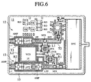
- Fig.6 is an external view showing the actual layout of a practical receiver/transmitter device in accordance with this embodiment.
- the base structure 15 is made up of copper in the form of a shallow bathtub in which the substrate as illustrated in Fig.3 is attached to.
- the circuit board structure 11 consisting of the transmitter circuit 12 (a voltage-controlled oscillator), the receiver circuit 13 and the local oscillator 14 as well as some auxiliary circuits which are not explained since they are not important.
- the through halls sequences T1, T2, R1, R2, L1 and L2 in order to section the transmitter circuit 12, the receiver circuit 13 and the local oscillator 14.
- the transmitter circuit, the receiver circuit and the local oscillator are formed on a common substrate between the ground electrodes and segmented by means of the through hall sequences. For this reason, even in the case that there is a substantial differential level between the transmission electric power and the reception electric power, it is possible to effectively isolate the circuits from each other. As a result, it is possible to realize the receiver/transmitter apparatus which is advantageous in the massproductivity and the miniaturization.
Landscapes
- Engineering & Computer Science (AREA)
- Computer Networks & Wireless Communication (AREA)
- Signal Processing (AREA)
- Physics & Mathematics (AREA)
- Electromagnetism (AREA)
- Microelectronics & Electronic Packaging (AREA)
- Transmitters (AREA)
- Transceivers (AREA)
Applications Claiming Priority (4)
| Application Number | Priority Date | Filing Date | Title |
|---|---|---|---|
| JP26370099 | 1999-09-17 | ||
| JP26369899 | 1999-09-17 | ||
| JP26370099A JP2001086023A (ja) | 1999-09-17 | 1999-09-17 | 送受信装置 |
| JP26369899A JP2001086022A (ja) | 1999-09-17 | 1999-09-17 | 送受信装置 |
Publications (2)
| Publication Number | Publication Date |
|---|---|
| EP1085666A2 true EP1085666A2 (de) | 2001-03-21 |
| EP1085666A3 EP1085666A3 (de) | 2003-10-29 |
Family
ID=26546147
Family Applications (1)
| Application Number | Title | Priority Date | Filing Date |
|---|---|---|---|
| EP00119474A Ceased EP1085666A3 (de) | 1999-09-17 | 2000-09-15 | Funksendeempfänger |
Country Status (2)
| Country | Link |
|---|---|
| US (1) | US6628925B1 (de) |
| EP (1) | EP1085666A3 (de) |
Families Citing this family (6)
| Publication number | Priority date | Publication date | Assignee | Title |
|---|---|---|---|---|
| US6876836B2 (en) * | 2002-07-25 | 2005-04-05 | Integrated Programmable Communications, Inc. | Layout of wireless communication circuit on a printed circuit board |
| DE60322488D1 (de) * | 2002-09-27 | 2008-09-11 | Fujitsu Ltd | Funkgerät für Freilufteinsatz |
| US7113750B2 (en) * | 2002-12-16 | 2006-09-26 | Tektronix, Inc. | Apparatus and method for input channel isolation within an electronic test instrument |
| JP4029779B2 (ja) * | 2003-06-05 | 2008-01-09 | 株式会社村田製作所 | 高周波モジュールおよび通信装置 |
| JP4553627B2 (ja) * | 2004-04-30 | 2010-09-29 | 太陽誘電株式会社 | 高周波回路モジュールおよび無線通信機器 |
| JP2012095282A (ja) * | 2010-10-01 | 2012-05-17 | Mitsumi Electric Co Ltd | 無線通信装置 |
Family Cites Families (4)
| Publication number | Priority date | Publication date | Assignee | Title |
|---|---|---|---|---|
| US5239685A (en) * | 1991-10-08 | 1993-08-24 | Qualcomm Incorporated | Process for fabricating a MMIC hybrid device and a transceiver fabricated thereby |
| JP2840493B2 (ja) * | 1991-12-27 | 1998-12-24 | 株式会社日立製作所 | 一体型マイクロ波回路 |
| GB2282270B (en) * | 1993-03-31 | 1996-12-04 | Motorola Inc | Switch circuit and method therefor |
| JP3252653B2 (ja) * | 1995-06-05 | 2002-02-04 | 三菱電機株式会社 | 送受信機 |
-
2000
- 2000-09-15 EP EP00119474A patent/EP1085666A3/de not_active Ceased
- 2000-09-15 US US09/662,703 patent/US6628925B1/en not_active Expired - Fee Related
Non-Patent Citations (3)
| Title |
|---|
| HENDERSON R. M.; KATEHI, L. P. B.: "Silicon-Based Micromachined Packages for Discrete Components", MICROWAVE SYMPOSIUM DIGEST, 1997, IEEE MTT-S INTERNATIONAL, vol. 2, 8 June 1997 (1997-06-08), DENVER, CO, USA, pages 521 - 524, XP010228478 * |
| ROBINSON, A.L.; MO, J.-H.: "Applications of Microelectronics and Microfabrication to Ultrasound Imaging Systems", ULTRASONICS SYMPOSIUM, 1992, PROCEEDINGS, IEEE, 20 October 1992 (1992-10-20), TUCSON, AZ, USA, pages 681 - 691, XP010103708 * |
| SHIH, Y.C.; LI, K.; KASEL, K.; FONG, L.; HOLZ, G.; SHALKAHAUSER, K.: "A High Performance Quartz Package for Millimeter-Wave Applications", MICROWAVE SYMPOSIUM DIGEST, 1991, IEEE, MTT-S INTERNATIONAL, 10 June 1991 (1991-06-10), BOSTON, MA, USA, pages 1063 - 1066, XP010037815 * |
Also Published As
| Publication number | Publication date |
|---|---|
| US6628925B1 (en) | 2003-09-30 |
| EP1085666A3 (de) | 2003-10-29 |
Similar Documents
| Publication | Publication Date | Title |
|---|---|---|
| US5671220A (en) | Satellite channel interface in indoor unit used for satellite data communication | |
| RU2295809C2 (ru) | Печатная антенна с питанием от коммутационного поля печатной платы | |
| US7015862B2 (en) | Antenna, method for manufacturing the antenna, and communication apparatus including the antenna | |
| EP1025614B1 (de) | Kompakte antennenstrukturen mit symmetrierschaltungen | |
| US5644277A (en) | Three-wire-line vertical interconnect structure for multilevel substrates | |
| US6765455B1 (en) | Multi-layered spiral couplers on a fluropolymer composite substrate | |
| JP6112570B2 (ja) | 非接触コネクタ | |
| KR100867457B1 (ko) | 반도체 기판 및 집적 통신 회로 | |
| TW364227B (en) | Low cost high performance portable phase array antenna system for satellite communication | |
| US4721962A (en) | Antenna for a transceiver, particularly portable telephone | |
| US20070066243A1 (en) | Rf circuit module | |
| US20020175784A1 (en) | Transmission line, integrated circuit, and transmitter receiver | |
| US6738598B2 (en) | Multilayer radio frequency interconnect system | |
| KR970008294B1 (ko) | 고주파 전력 분할회로 | |
| US6628925B1 (en) | Receiver/transmitter apparatus | |
| US6816028B2 (en) | Multilayer substrate and satellite broadcast reception apparatus | |
| JP2003008311A (ja) | バランおよび該バランを有する半導体装置 | |
| US10950947B2 (en) | Antenna feed elements with constant inverted phase | |
| CN111082819B (zh) | 一种消弱射频多通道间耦合的装置 | |
| EP1683229B1 (de) | Verlustarmer koppler mit suspendiertem substrat | |
| US6759920B1 (en) | Multi-layer balun transformer | |
| US6400241B1 (en) | Microwave circuit module and a device for connecting it to another module | |
| JP6575677B2 (ja) | フロントエンド回路、および、高周波モジュール | |
| US20240154300A1 (en) | System | |
| CN101283518B (zh) | 射频开关 |
Legal Events
| Date | Code | Title | Description |
|---|---|---|---|
| PUAI | Public reference made under article 153(3) epc to a published international application that has entered the european phase |
Free format text: ORIGINAL CODE: 0009012 |
|
| 17P | Request for examination filed |
Effective date: 20000915 |
|
| AK | Designated contracting states |
Kind code of ref document: A2 Designated state(s): AT BE CH CY DE DK ES FI FR GB GR IE IT LI LU MC NL PT SE |
|
| AX | Request for extension of the european patent |
Free format text: AL;LT;LV;MK;RO;SI |
|
| PUAL | Search report despatched |
Free format text: ORIGINAL CODE: 0009013 |
|
| AK | Designated contracting states |
Kind code of ref document: A3 Designated state(s): AT BE CH CY DE DK ES FI FR GB GR IE IT LI LU MC NL PT SE |
|
| AX | Request for extension of the european patent |
Extension state: AL LT LV MK RO SI |
|
| RIC1 | Information provided on ipc code assigned before grant |
Ipc: 7H 04B 1/38 B Ipc: 7H 04B 1/44 B Ipc: 7H 04B 1/40 A |
|
| 17Q | First examination report despatched |
Effective date: 20040204 |
|
| AKX | Designation fees paid |
Designated state(s): DE FR GB |
|
| APBN | Date of receipt of notice of appeal recorded |
Free format text: ORIGINAL CODE: EPIDOSNNOA2E |
|
| APBR | Date of receipt of statement of grounds of appeal recorded |
Free format text: ORIGINAL CODE: EPIDOSNNOA3E |
|
| APAF | Appeal reference modified |
Free format text: ORIGINAL CODE: EPIDOSCREFNE |
|
| APBT | Appeal procedure closed |
Free format text: ORIGINAL CODE: EPIDOSNNOA9E |
|
| STAA | Information on the status of an ep patent application or granted ep patent |
Free format text: STATUS: THE APPLICATION HAS BEEN REFUSED |
|
| 18R | Application refused |
Effective date: 20051122 |
|
| R18R | Application refused (corrected) |
Effective date: 20080314 |