EP1087365A2 - Elektrolumineszierende Anzeigevorrichtung und Steuerungsverfahren dafür - Google Patents
Elektrolumineszierende Anzeigevorrichtung und Steuerungsverfahren dafür Download PDFInfo
- Publication number
- EP1087365A2 EP1087365A2 EP00120759A EP00120759A EP1087365A2 EP 1087365 A2 EP1087365 A2 EP 1087365A2 EP 00120759 A EP00120759 A EP 00120759A EP 00120759 A EP00120759 A EP 00120759A EP 1087365 A2 EP1087365 A2 EP 1087365A2
- Authority
- EP
- European Patent Office
- Prior art keywords
- digital data
- image information
- bit
- bit digital
- display device
- Prior art date
- Legal status (The legal status is an assumption and is not a legal conclusion. Google has not performed a legal analysis and makes no representation as to the accuracy of the status listed.)
- Granted
Links
Images


Classifications
-
- G—PHYSICS
- G09—EDUCATION; CRYPTOGRAPHY; DISPLAY; ADVERTISING; SEALS
- G09G—ARRANGEMENTS OR CIRCUITS FOR CONTROL OF INDICATING DEVICES USING STATIC MEANS TO PRESENT VARIABLE INFORMATION
- G09G5/00—Control arrangements or circuits for visual indicators common to cathode-ray tube indicators and other visual indicators
- G09G5/02—Control arrangements or circuits for visual indicators common to cathode-ray tube indicators and other visual indicators characterised by the way in which colour is displayed
-
- G—PHYSICS
- G09—EDUCATION; CRYPTOGRAPHY; DISPLAY; ADVERTISING; SEALS
- G09G—ARRANGEMENTS OR CIRCUITS FOR CONTROL OF INDICATING DEVICES USING STATIC MEANS TO PRESENT VARIABLE INFORMATION
- G09G3/00—Control arrangements or circuits, of interest only in connection with visual indicators other than cathode-ray tubes
- G09G3/20—Control arrangements or circuits, of interest only in connection with visual indicators other than cathode-ray tubes for presentation of an assembly of a number of characters, e.g. a page, by composing the assembly by combination of individual elements arranged in a matrix no fixed position being assigned to or needed to be assigned to the individual characters or partial characters
- G09G3/22—Control arrangements or circuits, of interest only in connection with visual indicators other than cathode-ray tubes for presentation of an assembly of a number of characters, e.g. a page, by composing the assembly by combination of individual elements arranged in a matrix no fixed position being assigned to or needed to be assigned to the individual characters or partial characters using controlled light sources
- G09G3/30—Control arrangements or circuits, of interest only in connection with visual indicators other than cathode-ray tubes for presentation of an assembly of a number of characters, e.g. a page, by composing the assembly by combination of individual elements arranged in a matrix no fixed position being assigned to or needed to be assigned to the individual characters or partial characters using controlled light sources using electroluminescent panels
-
- G—PHYSICS
- G09—EDUCATION; CRYPTOGRAPHY; DISPLAY; ADVERTISING; SEALS
- G09G—ARRANGEMENTS OR CIRCUITS FOR CONTROL OF INDICATING DEVICES USING STATIC MEANS TO PRESENT VARIABLE INFORMATION
- G09G3/00—Control arrangements or circuits, of interest only in connection with visual indicators other than cathode-ray tubes
- G09G3/20—Control arrangements or circuits, of interest only in connection with visual indicators other than cathode-ray tubes for presentation of an assembly of a number of characters, e.g. a page, by composing the assembly by combination of individual elements arranged in a matrix no fixed position being assigned to or needed to be assigned to the individual characters or partial characters
- G09G3/2007—Display of intermediate tones
- G09G3/2018—Display of intermediate tones by time modulation using two or more time intervals
- G09G3/2022—Display of intermediate tones by time modulation using two or more time intervals using sub-frames
- G09G3/2037—Display of intermediate tones by time modulation using two or more time intervals using sub-frames with specific control of sub-frames corresponding to the least significant bits
-
- G—PHYSICS
- G09—EDUCATION; CRYPTOGRAPHY; DISPLAY; ADVERTISING; SEALS
- G09G—ARRANGEMENTS OR CIRCUITS FOR CONTROL OF INDICATING DEVICES USING STATIC MEANS TO PRESENT VARIABLE INFORMATION
- G09G3/00—Control arrangements or circuits, of interest only in connection with visual indicators other than cathode-ray tubes
- G09G3/20—Control arrangements or circuits, of interest only in connection with visual indicators other than cathode-ray tubes for presentation of an assembly of a number of characters, e.g. a page, by composing the assembly by combination of individual elements arranged in a matrix no fixed position being assigned to or needed to be assigned to the individual characters or partial characters
- G09G3/22—Control arrangements or circuits, of interest only in connection with visual indicators other than cathode-ray tubes for presentation of an assembly of a number of characters, e.g. a page, by composing the assembly by combination of individual elements arranged in a matrix no fixed position being assigned to or needed to be assigned to the individual characters or partial characters using controlled light sources
- G09G3/30—Control arrangements or circuits, of interest only in connection with visual indicators other than cathode-ray tubes for presentation of an assembly of a number of characters, e.g. a page, by composing the assembly by combination of individual elements arranged in a matrix no fixed position being assigned to or needed to be assigned to the individual characters or partial characters using controlled light sources using electroluminescent panels
- G09G3/32—Control arrangements or circuits, of interest only in connection with visual indicators other than cathode-ray tubes for presentation of an assembly of a number of characters, e.g. a page, by composing the assembly by combination of individual elements arranged in a matrix no fixed position being assigned to or needed to be assigned to the individual characters or partial characters using controlled light sources using electroluminescent panels semiconductive, e.g. using light-emitting diodes [LED]
- G09G3/3208—Control arrangements or circuits, of interest only in connection with visual indicators other than cathode-ray tubes for presentation of an assembly of a number of characters, e.g. a page, by composing the assembly by combination of individual elements arranged in a matrix no fixed position being assigned to or needed to be assigned to the individual characters or partial characters using controlled light sources using electroluminescent panels semiconductive, e.g. using light-emitting diodes [LED] organic, e.g. using organic light-emitting diodes [OLED]
- G09G3/3225—Control arrangements or circuits, of interest only in connection with visual indicators other than cathode-ray tubes for presentation of an assembly of a number of characters, e.g. a page, by composing the assembly by combination of individual elements arranged in a matrix no fixed position being assigned to or needed to be assigned to the individual characters or partial characters using controlled light sources using electroluminescent panels semiconductive, e.g. using light-emitting diodes [LED] organic, e.g. using organic light-emitting diodes [OLED] using an active matrix
- G09G3/3258—Control arrangements or circuits, of interest only in connection with visual indicators other than cathode-ray tubes for presentation of an assembly of a number of characters, e.g. a page, by composing the assembly by combination of individual elements arranged in a matrix no fixed position being assigned to or needed to be assigned to the individual characters or partial characters using controlled light sources using electroluminescent panels semiconductive, e.g. using light-emitting diodes [LED] organic, e.g. using organic light-emitting diodes [OLED] using an active matrix with pixel circuitry controlling the voltage across the light-emitting element
-
- G—PHYSICS
- G09—EDUCATION; CRYPTOGRAPHY; DISPLAY; ADVERTISING; SEALS
- G09G—ARRANGEMENTS OR CIRCUITS FOR CONTROL OF INDICATING DEVICES USING STATIC MEANS TO PRESENT VARIABLE INFORMATION
- G09G3/00—Control arrangements or circuits, of interest only in connection with visual indicators other than cathode-ray tubes
- G09G3/20—Control arrangements or circuits, of interest only in connection with visual indicators other than cathode-ray tubes for presentation of an assembly of a number of characters, e.g. a page, by composing the assembly by combination of individual elements arranged in a matrix no fixed position being assigned to or needed to be assigned to the individual characters or partial characters
- G09G3/22—Control arrangements or circuits, of interest only in connection with visual indicators other than cathode-ray tubes for presentation of an assembly of a number of characters, e.g. a page, by composing the assembly by combination of individual elements arranged in a matrix no fixed position being assigned to or needed to be assigned to the individual characters or partial characters using controlled light sources
- G09G3/30—Control arrangements or circuits, of interest only in connection with visual indicators other than cathode-ray tubes for presentation of an assembly of a number of characters, e.g. a page, by composing the assembly by combination of individual elements arranged in a matrix no fixed position being assigned to or needed to be assigned to the individual characters or partial characters using controlled light sources using electroluminescent panels
- G09G3/32—Control arrangements or circuits, of interest only in connection with visual indicators other than cathode-ray tubes for presentation of an assembly of a number of characters, e.g. a page, by composing the assembly by combination of individual elements arranged in a matrix no fixed position being assigned to or needed to be assigned to the individual characters or partial characters using controlled light sources using electroluminescent panels semiconductive, e.g. using light-emitting diodes [LED]
- G09G3/3208—Control arrangements or circuits, of interest only in connection with visual indicators other than cathode-ray tubes for presentation of an assembly of a number of characters, e.g. a page, by composing the assembly by combination of individual elements arranged in a matrix no fixed position being assigned to or needed to be assigned to the individual characters or partial characters using controlled light sources using electroluminescent panels semiconductive, e.g. using light-emitting diodes [LED] organic, e.g. using organic light-emitting diodes [OLED]
- G09G3/3275—Details of drivers for data electrodes
-
- G—PHYSICS
- G09—EDUCATION; CRYPTOGRAPHY; DISPLAY; ADVERTISING; SEALS
- G09G—ARRANGEMENTS OR CIRCUITS FOR CONTROL OF INDICATING DEVICES USING STATIC MEANS TO PRESENT VARIABLE INFORMATION
- G09G2300/00—Aspects of the constitution of display devices
- G09G2300/08—Active matrix structure, i.e. with use of active elements, inclusive of non-linear two terminal elements, in the pixels together with light emitting or modulating elements
- G09G2300/0809—Several active elements per pixel in active matrix panels
- G09G2300/0842—Several active elements per pixel in active matrix panels forming a memory circuit, e.g. a dynamic memory with one capacitor
-
- G—PHYSICS
- G09—EDUCATION; CRYPTOGRAPHY; DISPLAY; ADVERTISING; SEALS
- G09G—ARRANGEMENTS OR CIRCUITS FOR CONTROL OF INDICATING DEVICES USING STATIC MEANS TO PRESENT VARIABLE INFORMATION
- G09G2320/00—Control of display operating conditions
- G09G2320/02—Improving the quality of display appearance
- G09G2320/0242—Compensation of deficiencies in the appearance of colours
-
- G—PHYSICS
- G09—EDUCATION; CRYPTOGRAPHY; DISPLAY; ADVERTISING; SEALS
- G09G—ARRANGEMENTS OR CIRCUITS FOR CONTROL OF INDICATING DEVICES USING STATIC MEANS TO PRESENT VARIABLE INFORMATION
- G09G2320/00—Control of display operating conditions
- G09G2320/06—Adjustment of display parameters
- G09G2320/0666—Adjustment of display parameters for control of colour parameters, e.g. colour temperature
-
- G—PHYSICS
- G09—EDUCATION; CRYPTOGRAPHY; DISPLAY; ADVERTISING; SEALS
- G09G—ARRANGEMENTS OR CIRCUITS FOR CONTROL OF INDICATING DEVICES USING STATIC MEANS TO PRESENT VARIABLE INFORMATION
- G09G2320/00—Control of display operating conditions
- G09G2320/06—Adjustment of display parameters
- G09G2320/0673—Adjustment of display parameters for control of gamma adjustment, e.g. selecting another gamma curve
-
- G—PHYSICS
- G09—EDUCATION; CRYPTOGRAPHY; DISPLAY; ADVERTISING; SEALS
- G09G—ARRANGEMENTS OR CIRCUITS FOR CONTROL OF INDICATING DEVICES USING STATIC MEANS TO PRESENT VARIABLE INFORMATION
- G09G3/00—Control arrangements or circuits, of interest only in connection with visual indicators other than cathode-ray tubes
- G09G3/20—Control arrangements or circuits, of interest only in connection with visual indicators other than cathode-ray tubes for presentation of an assembly of a number of characters, e.g. a page, by composing the assembly by combination of individual elements arranged in a matrix no fixed position being assigned to or needed to be assigned to the individual characters or partial characters
- G09G3/2007—Display of intermediate tones
- G09G3/2018—Display of intermediate tones by time modulation using two or more time intervals
- G09G3/2022—Display of intermediate tones by time modulation using two or more time intervals using sub-frames
-
- G—PHYSICS
- G09—EDUCATION; CRYPTOGRAPHY; DISPLAY; ADVERTISING; SEALS
- G09G—ARRANGEMENTS OR CIRCUITS FOR CONTROL OF INDICATING DEVICES USING STATIC MEANS TO PRESENT VARIABLE INFORMATION
- G09G3/00—Control arrangements or circuits, of interest only in connection with visual indicators other than cathode-ray tubes
- G09G3/20—Control arrangements or circuits, of interest only in connection with visual indicators other than cathode-ray tubes for presentation of an assembly of a number of characters, e.g. a page, by composing the assembly by combination of individual elements arranged in a matrix no fixed position being assigned to or needed to be assigned to the individual characters or partial characters
- G09G3/22—Control arrangements or circuits, of interest only in connection with visual indicators other than cathode-ray tubes for presentation of an assembly of a number of characters, e.g. a page, by composing the assembly by combination of individual elements arranged in a matrix no fixed position being assigned to or needed to be assigned to the individual characters or partial characters using controlled light sources
- G09G3/30—Control arrangements or circuits, of interest only in connection with visual indicators other than cathode-ray tubes for presentation of an assembly of a number of characters, e.g. a page, by composing the assembly by combination of individual elements arranged in a matrix no fixed position being assigned to or needed to be assigned to the individual characters or partial characters using controlled light sources using electroluminescent panels
- G09G3/32—Control arrangements or circuits, of interest only in connection with visual indicators other than cathode-ray tubes for presentation of an assembly of a number of characters, e.g. a page, by composing the assembly by combination of individual elements arranged in a matrix no fixed position being assigned to or needed to be assigned to the individual characters or partial characters using controlled light sources using electroluminescent panels semiconductive, e.g. using light-emitting diodes [LED]
-
- G—PHYSICS
- G09—EDUCATION; CRYPTOGRAPHY; DISPLAY; ADVERTISING; SEALS
- G09G—ARRANGEMENTS OR CIRCUITS FOR CONTROL OF INDICATING DEVICES USING STATIC MEANS TO PRESENT VARIABLE INFORMATION
- G09G5/00—Control arrangements or circuits for visual indicators common to cathode-ray tube indicators and other visual indicators
- G09G5/02—Control arrangements or circuits for visual indicators common to cathode-ray tube indicators and other visual indicators characterised by the way in which colour is displayed
- G09G5/04—Control arrangements or circuits for visual indicators common to cathode-ray tube indicators and other visual indicators characterised by the way in which colour is displayed using circuits for interfacing with colour displays
Definitions
- the present invention relates to a method of driving an EL display device, a driving circuit for implementing the driving method, and an EL display device comprising the driving circuit.
- TFT thin film transistor
- This type of active matrix display device has been in the spotlight because of the many advantages which can be obtained by incorporating various circuits and elements on the same substrate, such as reduced manufacturing cost, display device miniaturization, increased yield, and higher throughput.
- An EL display device is also referred to as an organic EL display (OELD) or an organic light emitting diode (OLED).
- OELD organic EL display
- OLED organic light emitting diode
- an EL display device is of a self-light-emitting type.
- An EL element is structured such that an EL layer is sandwiched between a pair of electrodes.
- the EL layer typically has a laminated structure.
- a laminated structure of "a hole transporting layer / a light emitting layer / an electron transporting layer" proposed by Tang, et al. of Eastman Kodak Co. is a typical laminated structure. This structure has very high light emitting efficiency, and thus, most of EL display devices that are now under research and development adopt this structure.
- the laminated structure may be a hole injecting layer / a hole transporting layer / a light emitting layer / an electron transporting layer, or, a hole injecting layer / a hole transporting layer / a light emitting layer / an electron transporting layer / an electron injecting layer laminated in this order on a pixel electrode.
- a fluorescent pigment or the like may be doped in an EL layer.
- Color display methods of an EL display device are roughly divided into four: a method where three kinds of EL elements emitting R (red), G (green), and B (blue) light, respectively, are formed; a method where EL elements emitting white light are combined with a color filter of R, G, and B; a method where EL elements emitting blue or blue-green light are combined with a fluophor (fluorescent color conversion layer: CCM); and a method where EL elements corresponding to R, G, and B are superimposed on a transparent electrode used as a cathode (an opposing electrode).
- the luminance of red light emission is lower than the luminance of blue and green light emission in many organic EL materials.
- an organic EL material having such light emitting characteristics is used for an EL display device, the luminance of red in a displayed image is low.
- a method is conventionally adopted where orange light the wavelength of which is a little shorter than that of red light is used as red light.
- the luminance of red itself of an image displayed on the EL display device is low, and an image which is intended to be displayed in red is displayed in orange.
- a display device which has unbalanced luminance of red, green, and blue light emission and unsatisfactory white balance, can be provided.
- the present invention has been made in view of the above problems, and an object of the present invention is to provide a driving method and a driving circuit for realizing an EL display device with excellent white balance.
- a method of driving an EL display device is now described.
- the driving method according to the present invention in view of the lower luminance of red light emission of the EL light emitting layer, by suppressing the luminance of a green image and the luminance of a blue image, the luminance of a red image, the luminance of a green image, and the luminance of a blue image are well-balanced, which makes it possible to improve the white balance.
- the present invention can be applied not only to EL light emitting elements using an EL light emitting layer which emits white light and a color filter but also to EL light emitting elements using an EL light emitting layer which emits red light, an EL light emitting layer which emits green light, and an EL light emitting layer which emits blue light.
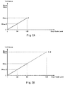
- Fig. 1 shows the luminance of red (R) light emission, the luminance of green (G) light emission, and the luminance of blue (B) light emission of EL light emitting elements with respect to gray-scale levels of the 6 bit digital data.
- the driving method according to the present invention can also be applied to a case where n bit digital data is inputted (n is a natural number).
- the luminance of red light emission, the luminance of green light emission, and the luminance of blue light emission take the maximum values B Rmax , B Gmax , and B Bmax , respectively.
- the maximum value B Rmax of the luminance of red light emission is half of the maximum value B Gmax of the luminance of green light emission or half of the maximum value B Bmax of the luminance of blue light emission, if the display is carried out with them being as they are, the maximum luminance varies and the white balance is unsatisfactory.
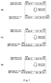
- Figs. 2 and 3 are conceptual views of the method of driving an EL display device according to the present invention.
- n bit digital data having red, green, and blue image information are converted into (n+1) bit digital data, respectively.
- n bit digital data having red, green, and blue image information (gray-scale information) are converted into (n+1) bit digital data, respectively.
- a case where 6 bit digital data are converted into 7 bit digital data is described as an example.
- digital data conversion carried out in the driving method according to the present invention is described with reference to Fig. 3.
- Data conversion of 6 bit digital data having red image information is shown in Fig. 3R
- data conversion of 6 bit digital data having green image information is shown in Fig. 3G
- data conversion of 6 bit digital data having blue image information is shown in Fig. 3B.
- the 6 bit digital data before the conversion is used as the upper 6 bits of the 7 bit digital data after the conversion. In this way, the 6 bit digital data having red image information is converted into the 7 bit digital data in which the value of the least significant bit (LSB) is "1".
- the 6 bit digital data before the conversion (G6 (MSB), G5, G4, G3, G2, and G1 (LSB)) is used as the lower 6 bits of the 7 bit digital data after the conversion. In this way, the 6 bit digital data having green image information is converted into the 7 bit digital data in which the value of the most significant bit (MSB) is "0".
- FIG. 3B data conversion of 6 bit digital data having blue image information (gray-scale information) (Fig. 3B) is described.
- the conversion of the 6 bit digital data having blue image information is similar to the conversion of the 6 bit digital data having green image information.
- the 6 bit digital data before the conversion (B6 (MSB), B5, B4, B3, B2, and B1 (LSB)) is used as the lower 6 bits of the 7 bit digital data after the conversion.
- the 6 bit digital data having blue image information is converted into the 7 bit digital data in which the value of the most significant bit (MSB) is "0".
- the respective red, green, and blue 6 bit digital data are converted into 7 bit digital data.
- the digital data having red image information presents the lowest luminance (here, 0) at the lowest gray-scale level (here, gray-scale level 2), and presents the highest luminance B Rmax at the highest gray-scale level (here, gray-scale level 128).
- Display of 64 gray-scales from gray-scale level 2 to gray-scale level 128 can be carried out with two gray scale levels as one step and the luminance being from the lowest luminance to the highest luminance B Rmax .
- the digital data having green image information presents the lowest luminance (here, 0) at the lowest gray-scale level (here, gray-scale level 1), and presents the highest luminance B Rmax at the highest gray-scale level (here, gray-scale level 64).
- the highest gray-scale level is 64 because the bit of the value of the most significant bit becomes "0" through the above-described digital data conversion. In this way, display of 64 gray-scales from gray-scale level 1 to gray-scale level 64 can be carried out with the luminance being from the lowest luminance to the highest luminance B Rmax .
- the digital data having blue image information presents the lowest luminance (here, 0) at the lowest gray-scale level (here, gray-scale level 1), and presents the highest luminance B Rmax at the highest gray-scale level (here, gray-scale level 64).
- the highest gray-scale level is 64 because the value of the most significant bit becomes "0" through the above-described digital data conversion. In this way, display of 64 gray-scales from gray-scale level 1 to gray-scale level 64 can be carried out with the luminance being from the lowest luminance to the highest luminance B Rmax .
- all of the highest luminance of red, the highest luminance of green, and the highest luminance of blue are the highest luminance B Rmax of red, and thus, display can be carried out with the luminance of red, the luminance of green, and the luminance of blue being well-balanced.
- n bit digital data having red image information (gray-scale information)
- n bit digital data having green image information (gray-scale information)
- n bit digital data having blue image information (gray-scale information)
- n bit digital data having red image information is shown in Fig. 7R
- data conversion of n bit digital data having green image information is shown in Fig. 7G
- data conversion of n bit digital data having blue image information is shown in Fig. 7B.
- n bit digital data having red image information (gray-scale information) (Fig. 7R) is described.
- the n bit digital data before the conversion (Rn(MSB), Rn-1, ..., R3, R2, and R1 (LSB)) is used as the upper n bits of the (n+1) bit digital data after the conversion.
- the n bit digital data having red image information is converted into the (n+1) bit digital data in which the value of the least significant bit (LSB) is "1".
- n bit digital data having green image information (gray-scale information) (Fig. 7G)
- the n bit digital data before the conversion (Gn (MSB), Gn-1, ..., G3, G2, and G1 (LSB)) is used as the lower a bits of the (n+1) bit digital data after the conversion.
- the n bit digital data having green image information is converted into the (n+1) bit digital data in which the value of the most significant bit (MSB) is "0".
- n bit digital data having blue image information (gray-scale information) (Fig. 7B)
- the conversion of the n bit digital data having blue image information is similar to the conversion of the n bit digital data having green image information.
- n bit digital data before the conversion (Bn (MSB), Bn-1, ..., B3, B2, and B1 (LSB)) is used as the lower n bits of the (n+1) bit digital data after the conversion.
- the n bit digital data having blue image information is converted into the (n+1) bit digital data in which the value of the most significant bit (MSB) is "0".
- the respective red, green, and blue n bit digital data are converted into (n+1) bit digital data.
- Display of 2 n gray-scales from gray-scale level 2 to gray-scale level 2 n+1 can be carried out with two gray-scales as one step and with the luminance being from the lowest luminance to the highest luminance B Rmax .
- the highest gray-scale level is 2 n because the value of the most significant bit becomes "0" through the above-described digital data conversion. In this way, display of 2 n gray-scales from gray-scale level 1 to gray-scale level 2 n can be carried out with the luminance being from the lowest luminance to the highest luminance B Rmax .
- the highest gray-scale level is 2 n because the most significant bit of the data becomes "0" through the above-described digital data conversion. In this way, display of 2 n gray-scales from gray-scale level 1 to gray-scale level 2 n can be carried out with the luminance being from the lowest luminance to the highest luminance B Rmax .
- all of the highest luminance of red, the highest luminance of green, and the highest luminance of blue are the highest luminance B Rmax of red, and thus, display can be carried out with the luminance of red, the luminance of green, and the luminance of blue being well-balanced.
- one frame of an image is divided into seven subframes. It is to be noted that one cycle for inputting data to all the pixels in a display region of an EL display device is referred to as one frame.
- the frequency is 60 Hz. In other words, 60 frames are formed in one second. If the number of frames formed in one second is less than 60, flicker of an image is visually conspicuous. It is to be noted that a plurality of divisions of one frame are referred to as subframes.
- One subframe can be broken down into an address time period (Ta) and a sustain time period (Ts).
- An address time period is the whole time period necessary for inputting data to all the pixels in one subframe.
- a sustain time period (which may be called also as a lighting time period) is a time period during which the EL elements emit light.
- the first subframe is denoted as SF1
- the second to the seventh subframes are denoted as SF2 - SF7, respectively.
- the address time period (Ta) is constant with regard to all of SF1 - SF7.
- the sustain time period (Ts) of SF1 - SF7 are denoted as Ts1 - Ts7, respectively. It is to be noted that the display of SF1 corresponds to the most significant bit while the display of SF7 corresponds to the least significant bit.
- an opposing electrode an electrode which is not connected to TFTs, typically a cathode
- digital data is inputted to each of the pixels with the EL elements emitting no light.
- the time period to do this is an address time period.
- voltage is applied to the opposing electrode (the opposing electrode is selected) to make the EL elements emit light simultaneously.
- the time period to do this is a sustain time period.
- the time period to carry out the light emitting (to light the pixels) is any of the time periods Ts1 - Ts7.
- the sustain time period is any of the time periods Ts1 - Ts7.
- the gray-scale of a pixel can be controlled and desired luminance can be realized.
- n bit digital data is inputted from the external and is converted into (n+1) bit digital data as described in the above, first, one frame is divided into (n+1) subframes (denoted as SF1, SF2, SF3, ... SF(n-1), SF(n), and SF(n+1)) so as to correspond to the (n+1) bits.
- SF1, SF2, SF3, ... SF(n-1), SF(n), and SF(n+1) so as to correspond to the (n+1) bits.
- the number of divisions of one frame increases, which makes it necessary to drive a driving circuit at a higher frequency.
- Each of the (n+1) subframes can be broken down into an address time period (Ta) and a sustain time period (Ts). More specifically, by selecting whether voltage is applied to the opposing electrode common to all the EL elements or not, the address time period and the sustain time period are selected.
- pixels are sequentially selected (strictly speaking, TFTs for switching of the respective pixels are selected) to apply predetermined gate voltage (corresponding to a data signal) to gate electrodes of TFTs for current controlling).
- predetermined gate voltage corresponding to a data signal
- an EL element of a pixel to which digital data to make conducting its TFT for current controlling is inputted emits light after an address time period ends for a sustain time period allotted to the subframe. In other words, predetermined pixels are lighted.
- the gray-scales of the respective pixels can be controlled.
- the gray-scale of the pixel is controlled depending on how long the pixel is lighted in the subframes (the number of sustain time periods the pixel goes through).
- An EL display device is characterized in that the device includes a circuit for converting n bit digital data having red image information, n bit digital data having green image information, and n bit digital data having blue image information (n is a natural number) inputted from the external into (n+1) bit digital data having red image information, (n+1) bit digital data having green image information, and (n+1) bit digital data having blue image information, respectively, and in that, by adding a bit having the value of one below the least significant bit of the n bit digital data having red image information, adding a bit having the value of zero above the most significant bit of the n bit digital data having green image information, and by adding a bit having the value of zero above the most significant bit of the n bit digital data having blue image information, the circuit produces the (n+1) bit digital data having red image information, the (n+1) bit digital data having green image information, and the (n+1) bit digital data having blue image information, respectively, to be used for displaying an image.
- n is a natural number
- a method of driving an EL display device comprises the steps of: adding a bit having the value of one below the least significant bit of n bit digital data having red image information inputted from the external; adding a bit having the value of zero above the most significant bit of n bit digital data having green image information inputted from the external; and adding a bit having the value of zero above the most significant bit of n bit digital data having blue image information inputted from the external, whereby producing (n+1) bit digital data having red image information, (n+1) bit digital data having green image information, and (n+1) bit digital data having blue image information, respectively; and inputting the (n+1) bit digital data having red image information, the (n+1) bit digital data having green image information, and the (n+1) bit digital data having blue image information to a time-division gray-scale data signal generating circuit, the time-division gray-scale data signal generating circuit dividing one frame into (n+1) subframes (SF1, SF2, SF
- SF (n-1), SF(n), and SF (n+1)) and selecting an address time period (T a ) and a sustain time period (Ts1, Ts2, Ts3, ... Ts(n-1), Ts(n), and Ts(n+1) for SF1, SF2, SF3, ... SF (n-1), SF(n), and SF (n+1), respectively) for each of the (n+1) subframes, the sustain time periods for the (n+1) subframes being set so that Ts1:Ts2:Ts3: ... :Ts(n-1):Ts(n):Ts(n+1) 2 0 :2 -1 :2 -2 : ... :2 -(n-2) :2 -(n-1) :2 -n .
- Fig. 5 is a schematic block diagram of an EL display device having a driving circuit, which employs a driving method in accordance with the present invention.
- 6 bit digital data having red, green, and blue image information are inputted from the external.
- n bit digital data having red, green, and blue image information may also be inputted from the external.
- a pixel portion 101, and, a driving circuit 102 on the side of data signals and a driving circuit 103 on the side of gate signals both of which are disposed on the periphery of the pixel portion 101, are formed with TFTs formed on a substrate.
- a pair of such driving circuits 102 on the side of data signals may be provided so as to sandwich the pixel portion 101
- a pair of such driving circuits 103 on the side of gate signals may be provided so as to sandwich the pixel portion 101.
- the driving circuit 102 on the side of data signals basically includes a shift register 102a, a latch (A) 102b, and a latch (B) 102c.
- a clock signal (CK) and a start pulse (SP) are inputted to the shift register 102a.
- Digital data digital data (digital data (R), digital data (G), and digital data (B)) are inputted to the latch (A) 102b, and a latch signal is inputted to the latch (B) 102c.
- data inputted to the pixel portion 101 is digital data. More specifically, digital data having information of either "0" or "1" is inputted as it is to the pixel portion 101.
- FIG. 6 is an enlarged view of a pixel 104.
- a TFT 105 for switching is connected to a gate wiring 106 for inputting a gate signal and to a data wiring (also referred to as a source wiring) 107 for inputting a data signal.
- a gate of a TFT 108 for current controlling is connected to a drain of the TFT 105 for switching.
- a drain of the TFT 108 for current controlling is connected to an EL element 109 while a source of the TFT 108 for current controlling is connected to a power source supply line 110.
- the EL element 109 is formed of an anode (a pixel electrode) connected to the TFT 108 for current controlling and a cathode (an opposing electrode) provided so as to oppose the anode with an EL layer sandwiched therebetween.
- the cathode is connected to a predetermined power source 111.
- a capacitor 112 is provided to maintain the gate voltage of the TFT 108 for current controlling when the TFT 105 for switching is in an unselected state (OFF state).
- the capacitor 112 is connected to the drain of the TFT 105 for switching and to the power source supply line 110.
- Digital data inputted to the pixel portion 101 structured as described in the above is produced by a time-division gray-scale data signal generating circuit 113 and a digital data converting circuit 114.
- 6 bit digital data (6 bit digital data (R), 6 bit digital data (G), and 6 bit digital data (B)) inputted from the external are converted into 7 bit digital data (7 bit digital data (R), 7 bit digital data (G), and 7 bit digital data (B)), respectively, by the digital data converting circuit 114. It is to be noted that the method of converting the digital data is as described in the above.
- the 7 bit digital data (7 bit digital data (R), 7 bit digital data (G), and 7 bit digital data (B)) produced by the digital data converting circuit 114 are inputted to the time-division gray-scale data signal generating circuit 113.
- the time-division gray-scale data signal generating circuit 113 is a circuit for converting 7 bit digital data into digital data for carrying out time-division gray-scale and for generating a timing pulse and the like necessary for carrying out time-division gray-scale display.
- the time-division gray-scale data signal generating circuit 113 may be provided outside the EL display device according to the present invention.
- digital data formed there is structured to be inputted to the EL display device according to the present invention.
- an electronic apparatus having as its display the EL display device according to the present invention includes the EL display device according to the present invention and the time-division gray-scale data signal generating circuit as different parts.
- the time-division gray-scale data signal generating circuit 113 may be mounted in the form of an IC chip or the like on the EL display device according to the present invention.
- digital data formed by the IC chip is structured to be inputted to the EL display device according to the present invention.
- an electronic apparatus having as its display the EL display device according to the present invention includes as its part the EL display device according to the present invention having the IC chip including the time-division gray-scale data signal generating circuit 113 mounted thereon.
- the time-division gray-scale data signal generating circuit 113 can be formed with a TFT on the substrate having the pixel portion 104, the driving circuit 102 on the side of data signals, and the driving circuit 103 on the side of gate signals formed thereon.
- the processing can be carried out on the substrate.
- the EL display device using the driving method according to the present invention (hereinafter referred to as "the EL display device according to the present invention") can be incorporated into various electronic equipment to be used.
- Such electronic equipment include a video camera, a digital camera, a head-mounted display (a goggle-type display), a game machine, a car navigation system, a personal computer, a personal digital assistant (such as a mobile computer, a portable telephone, or an electronic book).
- Fig. 9 shows examples of such electronic equipment.
- Fig. 9A shows a personal computer formed of a main body 7001, an image input portion 7002, an EL display device 7003 according to the present invention, and a keyboard 7004.
- Fig. 9B shows a video camera formed of a main body 7101, an EL display device 7102 according to the present invention, a voice input portion 7103, a control switch 7104, a battery 7105, and an image receiving portion 7106.
- Fig. 9C shows a mobile computer formed of a main body 7201, a camera portion 7202, an image receiving portion 7203, a control switch 7204, and an EL display device 7205 according to the present invention.
- Fig. 9D shows a goggle-type display formed of a main body 7301, an EL display device 7302 according to the present invention, and an arm portion 7303.
- Fig. 9E shows a player using a recording medium with a program recorded thereon (hereinafter referred to as a recording medium) formed of a main body 7401, an EL display device 7402 according to the present invention, a speaker portion 7403, a recording medium 7404, and a control switch 7405.
- a recording medium formed of a main body 7401, an EL display device 7402 according to the present invention, a speaker portion 7403, a recording medium 7404, and a control switch 7405.
- the apparatus uses a DVD (digital versatile disc), a CD, or the like as the recording medium. With the apparatus, one can enjoy music, a movie, a game, or the Internet.
- Fig. 9F shows a game machine formed of a main body 7501, an EL display device 7502 according to the present invention, another EL display device 7503 according to the present invention, a recording medium 7504, a controller 7505, a sensor portion 7506 for the main body, a sensor portion 7507, and a CPU portion 7508.
- the sensor portion 7506 for the main body and the sensor portion 7507 can sense infrared radiation emitted from the controller 7505 and the main body 7501, respectively.
- the application of the EL display device according to the present invention is very wide, and the EL display device can be applied to electronic apparatus of all fields.
- the white balance can be improved to carry out satisfactory display even with regard to an EL display device using an EL light emitting layer with low luminance of red light emission.
Landscapes
- Engineering & Computer Science (AREA)
- Physics & Mathematics (AREA)
- Computer Hardware Design (AREA)
- General Physics & Mathematics (AREA)
- Theoretical Computer Science (AREA)
- Control Of Indicators Other Than Cathode Ray Tubes (AREA)
- Electroluminescent Light Sources (AREA)
- Control Of El Displays (AREA)
Priority Applications (1)
| Application Number | Priority Date | Filing Date | Title |
|---|---|---|---|
| EP05025459.8A EP1638071B1 (de) | 1999-09-24 | 2000-09-22 | Elektrolumineszierende Anzeigevorrichtung |
Applications Claiming Priority (2)
| Application Number | Priority Date | Filing Date | Title |
|---|---|---|---|
| JP27136699 | 1999-09-24 | ||
| JP27136699 | 1999-09-24 |
Related Child Applications (1)
| Application Number | Title | Priority Date | Filing Date |
|---|---|---|---|
| EP05025459.8A Division EP1638071B1 (de) | 1999-09-24 | 2000-09-22 | Elektrolumineszierende Anzeigevorrichtung |
Publications (3)
| Publication Number | Publication Date |
|---|---|
| EP1087365A2 true EP1087365A2 (de) | 2001-03-28 |
| EP1087365A3 EP1087365A3 (de) | 2002-05-22 |
| EP1087365B1 EP1087365B1 (de) | 2005-11-30 |
Family
ID=17499080
Family Applications (2)
| Application Number | Title | Priority Date | Filing Date |
|---|---|---|---|
| EP05025459.8A Expired - Lifetime EP1638071B1 (de) | 1999-09-24 | 2000-09-22 | Elektrolumineszierende Anzeigevorrichtung |
| EP00120759A Expired - Lifetime EP1087365B1 (de) | 1999-09-24 | 2000-09-22 | Elektrolumineszierende Anzeigevorrichtung und Steuerungsverfahren dafür |
Family Applications Before (1)
| Application Number | Title | Priority Date | Filing Date |
|---|---|---|---|
| EP05025459.8A Expired - Lifetime EP1638071B1 (de) | 1999-09-24 | 2000-09-22 | Elektrolumineszierende Anzeigevorrichtung |
Country Status (6)
| Country | Link |
|---|---|
| US (2) | US6351077B1 (de) |
| EP (2) | EP1638071B1 (de) |
| KR (1) | KR100680517B1 (de) |
| CN (2) | CN1624749B (de) |
| DE (1) | DE60024382T2 (de) |
| TW (1) | TW482992B (de) |
Cited By (4)
| Publication number | Priority date | Publication date | Assignee | Title |
|---|---|---|---|---|
| EP1282099A2 (de) * | 2001-07-31 | 2003-02-05 | Lg Electronics Inc. | Einrichtung und Verfahren zur Steuerung einer lichtausstrahlenden Anzeige |
| EP1361560A3 (de) * | 2002-05-07 | 2009-03-18 | Kabushiki Kaisha Toyota Jidoshokki | Halbleiter-Treiberschaltung, Anzeigevorrichtung und Verfahren zur Einstellung der Helligkeitsverteilung einer Anzeigevorrichtung |
| CN101707044B (zh) * | 2002-09-05 | 2014-04-09 | 株式会社半导体能源研究所 | 发光器件及其驱动方法 |
| US9928782B2 (en) | 2015-04-29 | 2018-03-27 | Lg Display Co., Ltd. | Four-primary-color organic light emitting display and driving method thereof |
Families Citing this family (33)
| Publication number | Priority date | Publication date | Assignee | Title |
|---|---|---|---|---|
| JP2001092413A (ja) * | 1999-09-24 | 2001-04-06 | Semiconductor Energy Lab Co Ltd | El表示装置および電子装置 |
| US6587086B1 (en) * | 1999-10-26 | 2003-07-01 | Semiconductor Energy Laboratory Co., Ltd. | Electro-optical device |
| TW521237B (en) * | 2000-04-18 | 2003-02-21 | Semiconductor Energy Lab | Light emitting device |
| US6580657B2 (en) * | 2001-01-04 | 2003-06-17 | International Business Machines Corporation | Low-power organic light emitting diode pixel circuit |
| US6753654B2 (en) | 2001-02-21 | 2004-06-22 | Semiconductor Energy Laboratory Co., Ltd. | Light emitting device and electronic appliance |
| JP2002311921A (ja) * | 2001-04-19 | 2002-10-25 | Hitachi Ltd | 表示装置およびその駆動方法 |
| KR100796793B1 (ko) * | 2001-09-08 | 2008-01-22 | 삼성전자주식회사 | 유기 박막 전계 발광 표시 패널과 이를 이용한 유기 박막 전계 발광 표시 장치 |
| WO2003046871A1 (en) * | 2001-11-21 | 2003-06-05 | Silicon Display Incorporated | Method and system for driving a pixel with single pulse chains |
| JP2003308042A (ja) * | 2002-04-17 | 2003-10-31 | Hitachi Ltd | 画像表示装置 |
| JP2004004788A (ja) * | 2002-04-24 | 2004-01-08 | Seiko Epson Corp | 電子素子の制御回路、電子回路、電気光学装置、電気光学装置の駆動方法、及び電子機器、並びに電子素子の制御方法 |
| WO2003092165A1 (fr) | 2002-04-26 | 2003-11-06 | Toshiba Matsushita Display Technology Co., Ltd. | Circuits a semi-conducteur destines a commander par courant un affichage et affichage correspondant |
| JP4094919B2 (ja) * | 2002-07-18 | 2008-06-04 | 東北パイオニア株式会社 | 有機発光表示装置 |
| US7352133B2 (en) * | 2002-08-05 | 2008-04-01 | Semiconductor Energy Laboratory Co., Ltd. | Light emitting device |
| US11228735B2 (en) * | 2003-01-14 | 2022-01-18 | Tseng-Lu Chien | LED or laser project light has more than 1 functions |
| JP4085323B2 (ja) * | 2003-01-22 | 2008-05-14 | ソニー株式会社 | フラットディスプレイ装置及び携帯端末装置 |
| KR100567305B1 (ko) * | 2003-02-20 | 2006-04-04 | 산요덴키가부시키가이샤 | 컬러 발광 표시 장치 |
| JP4619289B2 (ja) | 2003-03-26 | 2011-01-26 | 株式会社半導体エネルギー研究所 | 表示装置及びその駆動方法、並びに電子機器 |
| CN1820295A (zh) * | 2003-05-07 | 2006-08-16 | 东芝松下显示技术有限公司 | El显示装置及其驱动方法 |
| KR100835028B1 (ko) | 2003-05-07 | 2008-06-03 | 도시바 마쯔시따 디스플레이 테크놀로지 컴퍼니, 리미티드 | 매트릭스형 표시 장치 |
| WO2004102516A1 (ja) * | 2003-05-16 | 2004-11-25 | Toshiba Matsushita Display Technology Co., Ltd. | アクティブマトリクス型表示装置及びデジタルアナログ変換器 |
| KR100568593B1 (ko) * | 2003-12-30 | 2006-04-07 | 엘지.필립스 엘시디 주식회사 | 평판 표시장치 및 그의 구동방법 |
| JP3985788B2 (ja) * | 2004-01-22 | 2007-10-03 | セイコーエプソン株式会社 | 電気光学装置及び電子機器 |
| KR100761156B1 (ko) * | 2004-02-03 | 2007-09-21 | 엘지전자 주식회사 | 일렉트로-루미네센스 표시소자의 구동장치 및 방법 |
| KR101058125B1 (ko) * | 2004-02-23 | 2011-08-24 | 삼성전자주식회사 | 화상 표시 방법 및 표시 장치와, 이의 구동 장치 및 방법 |
| US7295192B2 (en) * | 2004-05-04 | 2007-11-13 | Au Optronics Corporation | Compensating color shift of electro-luminescent displays |
| JP2006227337A (ja) * | 2005-02-18 | 2006-08-31 | Fuji Electric Holdings Co Ltd | 有機el表示装置およびその駆動方法 |
| KR100911979B1 (ko) * | 2008-03-13 | 2009-08-13 | 삼성모바일디스플레이주식회사 | 유기전계발광 표시장치 및 그의 구동방법 |
| KR100952837B1 (ko) * | 2008-07-28 | 2010-04-15 | 삼성모바일디스플레이주식회사 | 유기전계발광 표시장치 |
| US11476626B2 (en) | 2008-11-12 | 2022-10-18 | Aaron Chien | DC powered remote control LED light-bar assembly |
| US10509304B2 (en) | 2008-11-12 | 2019-12-17 | Tseng-Lu Chien | LED projection light has features |
| KR101773419B1 (ko) * | 2010-11-22 | 2017-09-01 | 삼성디스플레이 주식회사 | 데이터 보상 방법 및 이를 수행하는 표시 장치 |
| CN107610660B (zh) * | 2017-09-18 | 2019-08-09 | 惠科股份有限公司 | 一种显示装置的驱动方法及显示装置 |
| CN110517626B (zh) * | 2019-07-16 | 2020-10-09 | 上海景吾智能科技有限公司 | 一种提高led显示屏图像刷新率的方法及装置 |
Family Cites Families (12)
| Publication number | Priority date | Publication date | Assignee | Title |
|---|---|---|---|---|
| JPH02245793A (ja) * | 1989-03-20 | 1990-10-01 | Hitachi Ltd | マトリックス表示装置 |
| ATE261168T1 (de) * | 1992-10-15 | 2004-03-15 | Texas Instruments Inc | Anzeigevorrichtung |
| WO1996031865A1 (en) * | 1995-04-07 | 1996-10-10 | Fujitsu General Limited | Method of driving display device and its circuit |
| JPH0998443A (ja) * | 1995-09-29 | 1997-04-08 | Matsushita Electric Ind Co Ltd | 色補正装置 |
| US5812105A (en) * | 1996-06-10 | 1998-09-22 | Cree Research, Inc. | Led dot matrix drive method and apparatus |
| JP3645350B2 (ja) * | 1996-04-09 | 2005-05-11 | シチズン時計株式会社 | 表示装置 |
| TW441136B (en) | 1997-01-28 | 2001-06-16 | Casio Computer Co Ltd | An electroluminescent display device and a driving method thereof |
| JPH10312173A (ja) | 1997-05-09 | 1998-11-24 | Pioneer Electron Corp | 画像表示装置 |
| US5898415A (en) * | 1997-09-26 | 1999-04-27 | Candescent Technologies Corporation | Circuit and method for controlling the color balance of a flat panel display without reducing gray scale resolution |
| US6151001A (en) * | 1998-01-30 | 2000-11-21 | Electro Plasma, Inc. | Method and apparatus for minimizing false image artifacts in a digitally controlled display monitor |
| US6157396A (en) * | 1999-02-16 | 2000-12-05 | Pixonics Llc | System and method for using bitstream information to process images for use in digital display systems |
| JP4484276B2 (ja) * | 1999-09-17 | 2010-06-16 | 日立プラズマディスプレイ株式会社 | プラズマディスプレイ装置およびその表示方法 |
-
2000
- 2000-08-31 TW TW089117818A patent/TW482992B/zh not_active IP Right Cessation
- 2000-09-19 US US09/664,173 patent/US6351077B1/en not_active Expired - Lifetime
- 2000-09-22 EP EP05025459.8A patent/EP1638071B1/de not_active Expired - Lifetime
- 2000-09-22 DE DE60024382T patent/DE60024382T2/de not_active Expired - Lifetime
- 2000-09-22 EP EP00120759A patent/EP1087365B1/de not_active Expired - Lifetime
- 2000-09-23 CN CN2004101022339A patent/CN1624749B/zh not_active Expired - Fee Related
- 2000-09-23 CN CNB00128858XA patent/CN1188813C/zh not_active Expired - Fee Related
- 2000-09-25 KR KR1020000056220A patent/KR100680517B1/ko not_active Expired - Fee Related
-
2002
- 2002-01-02 US US10/039,788 patent/US6617799B2/en not_active Expired - Fee Related
Cited By (7)
| Publication number | Priority date | Publication date | Assignee | Title |
|---|---|---|---|---|
| EP1282099A2 (de) * | 2001-07-31 | 2003-02-05 | Lg Electronics Inc. | Einrichtung und Verfahren zur Steuerung einer lichtausstrahlenden Anzeige |
| US7636086B2 (en) | 2001-07-31 | 2009-12-22 | Lg Electronics Inc. | Circuit and method for driving self light-emitting display device |
| EP2251854A1 (de) * | 2001-07-31 | 2010-11-17 | LG Electronics Inc. | Einrichtung und Verfahren zur Steuerung einer lichtausstrahlenden Anzeige |
| EP1361560A3 (de) * | 2002-05-07 | 2009-03-18 | Kabushiki Kaisha Toyota Jidoshokki | Halbleiter-Treiberschaltung, Anzeigevorrichtung und Verfahren zur Einstellung der Helligkeitsverteilung einer Anzeigevorrichtung |
| CN101707044B (zh) * | 2002-09-05 | 2014-04-09 | 株式会社半导体能源研究所 | 发光器件及其驱动方法 |
| US9928782B2 (en) | 2015-04-29 | 2018-03-27 | Lg Display Co., Ltd. | Four-primary-color organic light emitting display and driving method thereof |
| EP3089151B1 (de) * | 2015-04-29 | 2023-05-31 | LG Display Co., Ltd. | Organische lichtemittierende anzeigevorrichtung mit vier primärfarben und verfahren zu ihrer ansteuerung |
Also Published As
| Publication number | Publication date |
|---|---|
| KR100680517B1 (ko) | 2007-02-09 |
| EP1638071A2 (de) | 2006-03-22 |
| CN1624749B (zh) | 2010-06-16 |
| US6617799B2 (en) | 2003-09-09 |
| US20020063536A1 (en) | 2002-05-30 |
| KR20010050632A (ko) | 2001-06-15 |
| TW482992B (en) | 2002-04-11 |
| DE60024382D1 (de) | 2006-01-05 |
| US6351077B1 (en) | 2002-02-26 |
| EP1638071A3 (de) | 2008-09-10 |
| CN1188813C (zh) | 2005-02-09 |
| EP1087365A3 (de) | 2002-05-22 |
| DE60024382T2 (de) | 2006-06-22 |
| EP1638071B1 (de) | 2017-03-08 |
| CN1292542A (zh) | 2001-04-25 |
| EP1087365B1 (de) | 2005-11-30 |
| CN1624749A (zh) | 2005-06-08 |
Similar Documents
| Publication | Publication Date | Title |
|---|---|---|
| EP1638071B1 (de) | Elektrolumineszierende Anzeigevorrichtung | |
| JP4024557B2 (ja) | 発光装置、電子機器 | |
| CN100385487C (zh) | 信号线驱动电路和发光装置 | |
| JP4244617B2 (ja) | 電気光学装置、電気光学装置の駆動方法 | |
| CN101231823A (zh) | 显示器件及包含这种显示器件的电子设备 | |
| JP2003271099A (ja) | 表示装置および表示装置の駆動方法 | |
| US7330162B2 (en) | Method of driving a light emitting device and electronic equipment | |
| JP2003108072A (ja) | 表示装置およびその駆動方法 | |
| JP4604455B2 (ja) | 電気光学装置、電気光学装置の駆動方法及び電子機器 | |
| JP2004163774A (ja) | 表示装置および表示装置の駆動方法 | |
| JP4757987B2 (ja) | El表示装置およびその駆動方法 | |
| JP5046657B2 (ja) | 表示装置 | |
| JP2003323157A (ja) | 発光装置の駆動方法及び電子機器 | |
| JP4397576B2 (ja) | 表示装置の駆動方法 | |
| JP2007122080A (ja) | 表示装置および表示装置の駆動方法 | |
| JP3889310B2 (ja) | 表示装置および表示装置の駆動方法 | |
| JP2003316322A (ja) | 発光装置及びその駆動方法 | |
| JP2004325749A (ja) | 有機elディスプレイの画像処理回路及びその駆動方法並びに電子機器 | |
| JP2006039510A (ja) | 半導体表示装置及び駆動方法 |
Legal Events
| Date | Code | Title | Description |
|---|---|---|---|
| PUAI | Public reference made under article 153(3) epc to a published international application that has entered the european phase |
Free format text: ORIGINAL CODE: 0009012 |
|
| AK | Designated contracting states |
Kind code of ref document: A2 Designated state(s): AT BE CH CY DE DK ES FI FR GB GR IE IT LI LU MC NL PT SE |
|
| AX | Request for extension of the european patent |
Free format text: AL;LT;LV;MK;RO;SI |
|
| PUAL | Search report despatched |
Free format text: ORIGINAL CODE: 0009013 |
|
| AX | Request for extension of the european patent |
Free format text: AL;LT;LV;MK;RO;SI |
|
| RIC1 | Information provided on ipc code assigned before grant |
Free format text: 7G 09G 3/32 A, 7G 09G 5/02 B |
|
| 17P | Request for examination filed |
Effective date: 20021108 |
|
| AKX | Designation fees paid |
Designated state(s): DE FI FR GB NL |
|
| 17Q | First examination report despatched |
Effective date: 20030204 |
|
| GRAP | Despatch of communication of intention to grant a patent |
Free format text: ORIGINAL CODE: EPIDOSNIGR1 |
|
| GRAS | Grant fee paid |
Free format text: ORIGINAL CODE: EPIDOSNIGR3 |
|
| GRAA | (expected) grant |
Free format text: ORIGINAL CODE: 0009210 |
|
| AK | Designated contracting states |
Kind code of ref document: B1 Designated state(s): DE FI FR GB NL |
|
| REG | Reference to a national code |
Ref country code: GB Ref legal event code: FG4D |
|
| REF | Corresponds to: |
Ref document number: 60024382 Country of ref document: DE Date of ref document: 20060105 Kind code of ref document: P |
|
| ET | Fr: translation filed | ||
| PLBE | No opposition filed within time limit |
Free format text: ORIGINAL CODE: 0009261 |
|
| STAA | Information on the status of an ep patent application or granted ep patent |
Free format text: STATUS: NO OPPOSITION FILED WITHIN TIME LIMIT |
|
| 26N | No opposition filed |
Effective date: 20060831 |
|
| PGFP | Annual fee paid to national office [announced via postgrant information from national office to epo] |
Ref country code: GB Payment date: 20120919 Year of fee payment: 13 Ref country code: FI Payment date: 20120912 Year of fee payment: 13 |
|
| PGFP | Annual fee paid to national office [announced via postgrant information from national office to epo] |
Ref country code: FR Payment date: 20120926 Year of fee payment: 13 |
|
| PGFP | Annual fee paid to national office [announced via postgrant information from national office to epo] |
Ref country code: NL Payment date: 20120908 Year of fee payment: 13 |
|
| REG | Reference to a national code |
Ref country code: NL Ref legal event code: V1 Effective date: 20140401 |
|
| PG25 | Lapsed in a contracting state [announced via postgrant information from national office to epo] |
Ref country code: FI Free format text: LAPSE BECAUSE OF NON-PAYMENT OF DUE FEES Effective date: 20130922 |
|
| GBPC | Gb: european patent ceased through non-payment of renewal fee |
Effective date: 20130922 |
|
| REG | Reference to a national code |
Ref country code: FR Ref legal event code: ST Effective date: 20140530 |
|
| PG25 | Lapsed in a contracting state [announced via postgrant information from national office to epo] |
Ref country code: GB Free format text: LAPSE BECAUSE OF NON-PAYMENT OF DUE FEES Effective date: 20130922 |
|
| PG25 | Lapsed in a contracting state [announced via postgrant information from national office to epo] |
Ref country code: FR Free format text: LAPSE BECAUSE OF NON-PAYMENT OF DUE FEES Effective date: 20130930 Ref country code: NL Free format text: LAPSE BECAUSE OF NON-PAYMENT OF DUE FEES Effective date: 20140401 |
|
| PGFP | Annual fee paid to national office [announced via postgrant information from national office to epo] |
Ref country code: DE Payment date: 20160913 Year of fee payment: 17 |
|
| REG | Reference to a national code |
Ref country code: DE Ref legal event code: R119 Ref document number: 60024382 Country of ref document: DE |
|
| PG25 | Lapsed in a contracting state [announced via postgrant information from national office to epo] |
Ref country code: DE Free format text: LAPSE BECAUSE OF NON-PAYMENT OF DUE FEES Effective date: 20180404 |