EP1087492A2 - Einschalt-Rücksetzschaltung - Google Patents
Einschalt-Rücksetzschaltung Download PDFInfo
- Publication number
- EP1087492A2 EP1087492A2 EP00125108A EP00125108A EP1087492A2 EP 1087492 A2 EP1087492 A2 EP 1087492A2 EP 00125108 A EP00125108 A EP 00125108A EP 00125108 A EP00125108 A EP 00125108A EP 1087492 A2 EP1087492 A2 EP 1087492A2
- Authority
- EP
- European Patent Office
- Prior art keywords
- reset
- electronic circuitry
- power supply
- power
- supply voltage
- Prior art date
- Legal status (The legal status is an assumption and is not a legal conclusion. Google has not performed a legal analysis and makes no representation as to the accuracy of the status listed.)
- Withdrawn
Links
Images

Classifications
-
- H—ELECTRICITY
- H02—GENERATION; CONVERSION OR DISTRIBUTION OF ELECTRIC POWER
- H02H—EMERGENCY PROTECTIVE CIRCUIT ARRANGEMENTS
- H02H3/00—Emergency protective circuit arrangements for automatic disconnection directly responsive to an undesired change from normal electric working condition with or without subsequent reconnection ; integrated protection
- H02H3/24—Emergency protective circuit arrangements for automatic disconnection directly responsive to an undesired change from normal electric working condition with or without subsequent reconnection ; integrated protection responsive to undervoltage or no-voltage
-
- H—ELECTRICITY
- H03—ELECTRONIC CIRCUITRY
- H03K—PULSE TECHNIQUE
- H03K17/00—Electronic switching or gating, i.e. not by contact-making and –breaking
- H03K17/22—Modifications for ensuring a predetermined initial state when the supply voltage has been applied
- H03K17/223—Modifications for ensuring a predetermined initial state when the supply voltage has been applied in field-effect transistor switches
-
- G—PHYSICS
- G11—INFORMATION STORAGE
- G11C—STATIC STORES
- G11C5/00—Details of stores covered by group G11C11/00
- G11C5/14—Power supply arrangements, e.g. power down, chip selection or deselection, layout of wirings or power grids, or multiple supply levels
- G11C5/143—Detection of memory cassette insertion or removal; Continuity checks of supply or ground lines; Detection of supply variations, interruptions or levels ; Switching between alternative supplies
-
- H—ELECTRICITY
- H02—GENERATION; CONVERSION OR DISTRIBUTION OF ELECTRIC POWER
- H02H—EMERGENCY PROTECTIVE CIRCUIT ARRANGEMENTS
- H02H3/00—Emergency protective circuit arrangements for automatic disconnection directly responsive to an undesired change from normal electric working condition with or without subsequent reconnection ; integrated protection
- H02H3/24—Emergency protective circuit arrangements for automatic disconnection directly responsive to an undesired change from normal electric working condition with or without subsequent reconnection ; integrated protection responsive to undervoltage or no-voltage
- H02H3/243—Emergency protective circuit arrangements for automatic disconnection directly responsive to an undesired change from normal electric working condition with or without subsequent reconnection ; integrated protection responsive to undervoltage or no-voltage for DC systems
-
- H—ELECTRICITY
- H03—ELECTRONIC CIRCUITRY
- H03K—PULSE TECHNIQUE
- H03K17/00—Electronic switching or gating, i.e. not by contact-making and –breaking
- H03K17/14—Modifications for compensating variations of physical values, e.g. of temperature
- H03K17/145—Modifications for compensating variations of physical values, e.g. of temperature in field-effect transistor switches
-
- H—ELECTRICITY
- H03—ELECTRONIC CIRCUITRY
- H03K—PULSE TECHNIQUE
- H03K17/00—Electronic switching or gating, i.e. not by contact-making and –breaking
- H03K17/22—Modifications for ensuring a predetermined initial state when the supply voltage has been applied
Definitions
- This invention relates to power-on reset circuits for holding electronic circuitry in reset when the supply voltage applied to the electronic circuitry is below a threshold voltage level and, in particular, to power-on reset circuits whose threshold voltage level is a function of the worst case device/component on the electronic circuitry.
- each electronic circuit requires some predetermined operating voltage range in order to operate properly. For example, an electronic circuit that requires a power supply of 5 volts may allow a voltage operating range of 4.5 volts to 5.5 volts for proper operation. However, if the power supply voltage falls below the 4.5 volts, the electronic circuit is not guaranteed to function properly, and if the power supply voltage rises above 5.5 volts, the electronic circuit may suffer irreversible damage.
- a reset signal typically exists for holding the electronic circuit in a reset state until the power supply voltage exceeds a predetermined threshold voltage. Additionally, if the power supply voltage falls below the threshold voltage, the electronic circuit should be placed back into the reset state. Failure to reset the electronic circuit when the power supply voltage is below the threshold voltage may result in the electronic circuit functioning inadequately thereby causing catastrophic results. For example, where a microcontroller is used in an anti-lock brake system, inadequate operation of the microcontroller due to a low power supply voltage could cause failure of the braking system. Accordingly, it is of utmost importance to take the electronic circuit out of reset and operate only when the power supply voltage exceeds the threshold voltage. Moreover, once taken out of reset, the electronic circuit must again be placed back into the reset state if the power supply voltage later falls below the threshold voltage.
- One scheme for resetting an electronic circuit upon start-up or power-on is to use external elements, such as resistors, capacitors and bipolar devices, to detect when the power supply voltage exceeds a predetermined threshold voltage.
- This scheme has the disadvantage that the predetermined threshold voltage is typically chosen to be an artificially high voltage level to insure that when the electronic circuit is taken out of reset, all of the various sub-circuits and devices in the electronic circuit are well within their proper operating voltage range.
- the overall operating voltage range of the electronic circuit is substantially decreased.
- Another scheme for holding an electronic circuit in a reset state upon power-on is to use a timer circuit, coupled for receiving the power supply voltage, including a capacitor that charges through a large resistor such that when the capacitor is filly charged, the electronic circuit is taken out of reset.
- this scheme provides only for a fixed time to hold the electronic circuit in reset while the voltage on power supply is ramping up and, thus, does not reliably handle slow power supply ramps. Accordingly, such schemes require a certain rise time specification on the power supply.
- Another more advanced scheme for holding an electronic circuit in a reset state upon power-on is to use a circuit that generates power-on reset signals when the power supply exceeds a fixed DC trip point threshold.
- Such circuits typically include a comparator having one of its inputs coupled to receive a band gap voltage and the other input coupled to receive a scaled version of the power supply voltage, via a resistor divider circuit, such that when the scaled version of the power supply voltage exceeds the band gap voltage, the comparator trips and allows the electronic circuit to be taken out of reset.
- the DC trip point threshold is generally chosen to be an artificially high voltage.
- the DC trip point threshold is difficult to pinpoint due to normal manufacturing variances of the circuit components such as the offset errors in the comparator.
- the worst case device/component i.e., the component that requires the highest supply voltage to operate properly
- the present invention provides a power-on reset circuit for resetting electronic circuitry coupled to the power-on reset circuit when a trip point generator representative of the worst case component within the electronic circuitry is detected to be operative.
- the power-on reset circuit of the present invention includes a trip point generator comprised of the worst case component of the electronic circuitry monitored where the worst case component is the component within the electronic circuitry that requires the highest supply voltage in order to operate properly. By assuring that the worst case component is operating properly, it is assured that all of the components on the electronic circuitry are also operating properly. Additionally, because the trip point generator of the present invention includes the worst case component of the electronic circuitry, the threshold voltage of the trip point generator will adequately track the electronic circuitry over normal process and temperature variations.
- the present invention provides the best possible voltage range for the electronic circuitry to be monitored with the guarantee that the electronic circuitry will not be taken out of reset before the power supply voltage exceeds a threshold voltage that is within the proper operating voltage range for all devices within the electronic circuitry regardless of process and temperature variation.
- the present invention does require one to ascertain the worst case component within the electronic circuitry to be monitored. Once this is obtained, however, it is assured that once the worst case component is operative, all components within the electronic circuitry are operative and the electronic circuitry can be taken out of reset.
- the ascertaining of the worst case device is fairly simple such as in the case where the electronic circuitry to be monitored takes the form of an electronically programmable read-only-memory (EPROM) memory.
- EPROM electronically programmable read-only-memory
- the worst case component is chosen to be an EPROM transistor because the transistors used in the EPROM memory cells have a threshold voltage substantially higher than the other transistors used in the process. In other cases, however, it may not be readily apparent which component is worst case. Therefore, two or more components may be used to set the threshold voltage whereby the power supply voltage must be at a sufficient voltage level to enable all the selected components to be operative before allowing the electronic circuitry to be taken out of reset.
- the present invention also includes a noise filter for placing the electronic circuitry back into reset if the power supply voltage falls below a predetermined threshold for at least a minimum period of time. In this manner, the present invention places the electronic circuitry back into reset in response to transient variations in the power supply voltage that go outside of the worst case device voltage range and are long enough to cause a device malfunction. However, very short voltage supply fluctuations that will not cause device failure are ignored
- the present invention provides a power-on reset circuit for resetting electronic circuitry coupled to the power-on reset circuit when a trip point generator representative of the worst case sub-circuit/device/component within the electronic circuitry is detected to be operative.
- the power-on reset circuit includes a trip point generator comprised of the worst case component of the electronic circuitry monitored where the worst case component is the component within the electronic circuitry that requires the highest supply voltage in order to operate properly.
- FIG. 1 a simplified block diagram illustrating power-on reset circuit 10 is shown.
- the reset circuit includes trip point generator 12 that is coupled to a power supply voltage terminal 13 at which a power supply operating voltage of V DD is applied.
- Trip point generator 12 includes the worst case device/component/sub-circuit (11) of the electronic circuitry (18) to be monitored such that when the worst case device becomes operative, a corresponding logic signal is generated indicative that the worst case component is now operative with the assurance that all devices within the electronic circuitry are also operative.
- the worst case component 11 may be either an actual isolated component from within the electronic circuitry thereby conserving size and power of the combined power-on reset circuit and the electronic circuitry, or it may be a duplicate/replica of the worst case component.
- Sensor 14 senses and detects when the worst case device of trip point generator 12 becomes operative and correspondingly provides a pulse on the power-on reset signal (signal POR) or alternately the complement or inversion thereof (a not power-on reset signal, or signal NPOR) to the electronic circuitry 18, via logic 16, for allowing the electronic circuitry to be taken out of reset since the operating voltage has achieved a predetermined threshold voltage level to allow the worst case device within electronic circuitry 18 to become operative.
- the power-on reset signal signal POR
- NPOR not power-on reset signal
- the power-on reset signal generated by sensor 14 is typically supplied to reset logic 16, which may be responsive to other signals, such as an external pin, a watch dog timer or an interrupt signal, for holding electronic circuitry 18 in reset whereby reset logic 16 supplies a reset signal to electronic circuitry 18.
- reset logic 16 supplies an active reset signal to electronic circuitry 18 to place circuitry 18 in a reset condition.
- the threshold voltage of the trip point generator adequately tracks electronic circuitry 18 over normal process and temperature variation so as to provide the optimum threshold voltage for allowing electronic circuitry 18 to be taken out of reset and for allowing for the maximum power supply operating range of electronic circuitry 18. Therefore, if process or temperature variations cause a change in the required power supply voltage threshold for worst case component 11 to operate properly, the trip point threshold voltage changes accordingly and electronic circuitry 18 is not taken out of reset until worst case component 11 is operative.
- the present invention provides the best possible voltage range for the electronic circuitry 18 with the guarantee that electronic circuitry 18 will not be taken out of reset before the power supply voltage exceeds a threshold voltage that is within the proper operating voltage range for all devices within electronic circuitry 18 regardless of process and temperature variation.
- the power-on reset signal of the present invention is not dependent upon the ramp rate of the power supply and, thus the present invention requires no power supply ramp rate specification for proper operation. Rather, the power-on reset signal is simply a function of when the worst case component becomes operative. Additionally, the present invention does not require the use of timers or the like.
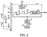
- FIG. 2 a more detailed schematic block diagram illustrating the power-on reset circuit of FIG. 1 is shown. It is understood that components shown in FIG. 2 that are identical to components shown in FIG. 1 are identified by like reference numbers.
- the embodiment of FIG. 2 comprises trip point generator 12 including electronically programmable read-only-memory (EPROM) transistor 22 for generating the trip point threshold voltage to be used for resetting EPROM 20.
- EPROM electronically programmable read-only-memory
- the worst case device is chosen to be EPROM transistor 22 because the transistors used in the EPROM memory cells have a threshold voltage substantially higher than the other transistors used in the process. Accordingly, when EPROM memory cell transistor 22 becomes operative, it is assured that all transistors and components within EPROM 20 are also operative.
- EPROM transistor 22 has a control/gate electrode coupled to receive power supply voltage V DD , and a source electrode returned to ground.
- Trip point generator 12 further includes transistors 24 and 26 as well as resistor 28.
- Transistor 24 has a source electrode coupled to the drain electrode of transistor 22 and drain electrode coupled to circuit node 28.
- the gate electrode of transistor 24 is coupled through resistor-configured transistor 26 to receive power supply voltage V DD -
- transistor 26 has a source electrode coupled to the gate electrode of transistor 24, a gate electrode returned to ground and a drain electrode coupled to receive power supply voltage V DD .
- circuit node 28 is coupled through resistor 27 to receive power supply voltage V DD .
- Sensor 14 senses and detects when EPROM transistor 22 becomes operative and generates a corresponding pulse to allow EPROM 20 to be taken out of reset (assuming that all the other conditions set by reset logic 16 are also satisfied).
- Sensor 14 includes NOR gate 30, AND gate 33, reset pulse generator 32 and noise filter 34.
- NOR gate 30 has a first input coupled to circuit node 28 and a second input coupled to the output of reset generator 32.
- the output of NOR gate 30 is coupled to a first input of AND gate 33 the output of which is supplied to an input of generator 32.
- the second input of AND gate 33 is coupled to an output of noise filter 34 the latter having an input coupled to the supply voltage terminal for receiving operating potential V DD .
- reset pulse generator 32 supplies not power-on reset signal (NPOR) to EPROM 20, via logic 16, wherein signal NPOR is a logic low when worst EPROM transistor 22 is non-operative thereby holding EPROM 20 in a reset condition and a logic high when transistor 22 is operative thereby allowing EPROM 20 to be taken out of reset.
- generator 32 provides a not power-on reset (NPOR) signal, it is understood that the inversion thereof, a power-on reset (POR) signal, could also be provided.
- reset pulse generator 32 In operation and upon voltage power-on, reset pulse generator 32 initially provides a logic low output thereby placing signal NPOR at a logic low ("0") level and holding EPROM 20 in .a reset condition. Accordingly, the second input of NOR gate 30 is at a logic "0". Moreover, the voltage at circuit node 28 is substantially equal to voltage V DD to thereby apply a logic "1" to the first input of NOR gate 30. In response, NOR gate 30 applies a logic "0" to the first input of AND gate 33.
- noise filter 34 is initialized to apply a logic" 1 "to the second input of NOR gate 33. Accordingly, AND gate 33 applies a logic "0" to the input of reset pulse generator 32 thereby holding the output of reset pulse generator 32 at a logic low and forcing the electronic circuitry to be monitored, in this case, EPROM 20, to remain in a reset condition.
- NOR gate 30 provides a logic "0" at the first input of NOR gate 33 which accordingly provides a logic low at the input of reset pulse generator 32 and causes the output of generator 32 to go low again and place EPROM 20 back into reset.
- the present invention includes noise filter 34 that monitors the power supply voltage after power-on to determine if the power supply has fallen below the threshold level set by the worst case device for a long enough time to cause damage to EPROM 20, but possibly not long enough to cause transistor 22 to turn off. In this manner, noise filter 34 responds to such mid-frequency noise that may cause failures within EPROM 20 of which may not be long enough to turn off transistor 22, but does not respond to high frequency noise that would not cause improper operation of EPROM 20.
- noise filter 34 includes simple circuitry (not shown) such that if the power supply voltage falls below a predetermined threshold for a predetermined amount of time to allow discharging of a capacitor, then noise filter 34 provides a logic "0" at its output. This provides a logic "0" at the input of reset pulse generator 32 thereby causing generator 32 to assert signal NPOR and reset EPROM 20.
- the present invention not only holds EPROM 20 in a reset condition until the power supply voltage has increased to a level such that the worst case component becomes operative, but it also includes noise filter 34 for placing the EPROM back into reset if the power supply voltage falls below a predetermined threshold for at least a minimum period of time.
- the present invention generally requires one to ascertain the worst case component within the electronic circuitry to be monitored. Once this is obtained, however, it is assured that once the worst case component is operative, all components within the electronic circuitry are operative and the circuitry can be taken out of reset. Ascertaining the worst case device of an electronic circuit may be fairly simple such as in the above embodiment where the electronic circuitry to be monitored was an EPROM memory device. In that case, the worst case component was ascertained to be an EPROM transistor because the transistors used in the EPROM memory cells have a threshold voltage substantially higher than the other transistors used in the process.
- trip point generator 12 includes serially-coupled transistors 41 and 42 coupled between a supply voltage terminal for receiving operating potential V DD and circuit node 44.
- transistor 41 is configured to operate as a diode whereby its drain and gate electrodes are coupled to receive the power supply voltage potential V DD while its source electrode coupled to the drain and gate electrodes of diode-configured transistor 42. Further, the source electrode of transistor 42 is coupled to circuit node 44 the later of which is returned to ground through resistor 46.
- Circuit node 44 is further coupled to the gate electrode of transistor 48 the latter of which has a drain electrode coupled to the first input of NOR gate 30 and through resistor 49 to receive power supply voltage V DD .
- the source electrode of transistor 48 is coupled to the drain electrode of transistor 50 the latter of which has a source electrode return to ground and a gate electrode coupled for receiving the power supply voltage V DD .
- both transistors 41 and 42 must become operative before the electronic circuitry is allowed to come out of reset.
- the power-on reset circuit includes a trip point generator including the worst case component (the component that requires the greatest power supply voltage to operate) within the electronic circuitry for setting the threshold voltage for taking the electronic circuitry out of reset such that if the worst case component is operative, it is guaranteed that all components are operative. Moreover, because the threshold voltage is based upon the worst case component of the electronic circuitry, the threshold voltage of the trip point generator will adequately track the electronic circuitry over normal process and temperature variations. Additionally, the power-on reset circuit includes a noise filter for placing the electronic circuitry back into reset if variations within the power supply voltage causes the power supply voltage level to fall below a predetermined threshold for at least a minimum period of time.
Landscapes
- Engineering & Computer Science (AREA)
- Power Engineering (AREA)
- Electronic Switches (AREA)
- Direct Current Feeding And Distribution (AREA)
- Emergency Protection Circuit Devices (AREA)
Applications Claiming Priority (3)
| Application Number | Priority Date | Filing Date | Title |
|---|---|---|---|
| US508332 | 1995-07-27 | ||
| US08/508,332 US5587866A (en) | 1995-07-27 | 1995-07-27 | Power-on reset circuit |
| EP96924422A EP0787379B1 (de) | 1995-07-27 | 1996-07-17 | Einschalt-rücksetzschaltung |
Related Parent Applications (1)
| Application Number | Title | Priority Date | Filing Date |
|---|---|---|---|
| EP96924422A Division EP0787379B1 (de) | 1995-07-27 | 1996-07-17 | Einschalt-rücksetzschaltung |
Publications (2)
| Publication Number | Publication Date |
|---|---|
| EP1087492A2 true EP1087492A2 (de) | 2001-03-28 |
| EP1087492A3 EP1087492A3 (de) | 2001-09-05 |
Family
ID=24022326
Family Applications (2)
| Application Number | Title | Priority Date | Filing Date |
|---|---|---|---|
| EP96924422A Expired - Lifetime EP0787379B1 (de) | 1995-07-27 | 1996-07-17 | Einschalt-rücksetzschaltung |
| EP00125108A Withdrawn EP1087492A3 (de) | 1995-07-27 | 1996-07-17 | Einschalt-Rücksetzschaltung |
Family Applications Before (1)
| Application Number | Title | Priority Date | Filing Date |
|---|---|---|---|
| EP96924422A Expired - Lifetime EP0787379B1 (de) | 1995-07-27 | 1996-07-17 | Einschalt-rücksetzschaltung |
Country Status (7)
| Country | Link |
|---|---|
| US (1) | US5587866A (de) |
| EP (2) | EP0787379B1 (de) |
| JP (1) | JPH10503920A (de) |
| KR (1) | KR100271951B1 (de) |
| DE (1) | DE69616266T2 (de) |
| TW (1) | TW293103B (de) |
| WO (1) | WO1997005683A1 (de) |
Families Citing this family (15)
| Publication number | Priority date | Publication date | Assignee | Title |
|---|---|---|---|---|
| US5778238A (en) * | 1996-06-19 | 1998-07-07 | Microchip Technology Incorporated | Power-down reset circuit |
| US6178501B1 (en) | 1998-04-28 | 2001-01-23 | Micron Technology. Inc. | Method and apparatus for initializing a memory device |
| US5978297A (en) * | 1998-04-28 | 1999-11-02 | Micron Technology, Inc. | Method and apparatus for strobing antifuse circuits in a memory device |
| US6181628B1 (en) | 1998-06-29 | 2001-01-30 | Cypress Semiconductor Corp. | Power-on-reset circuit with analog delay and high noise immunity |
| EP0986175A1 (de) * | 1998-09-08 | 2000-03-15 | EM Microelectronic-Marin SA | Einschalt-Rücksetzschaltung |
| US6970939B2 (en) * | 2000-10-26 | 2005-11-29 | Intel Corporation | Method and apparatus for large payload distribution in a network |
| US20050162794A1 (en) * | 2003-10-30 | 2005-07-28 | Donnelly David S. | System for mitigating radiation effects on componentry in space |
| US7450359B1 (en) * | 2005-03-03 | 2008-11-11 | National Semiconductor Corporation | System and method for providing a temperature compensated under-voltage-lockout circuit |
| US7711971B1 (en) * | 2006-06-28 | 2010-05-04 | Linear Technology Corporation | Multi-input power supply supervisor |
| TW200828001A (en) | 2006-12-25 | 2008-07-01 | Realtek Semiconductor Corp | Reset circuit and the associated method |
| CN102298951A (zh) * | 2010-06-25 | 2011-12-28 | 鸿富锦精密工业(深圳)有限公司 | 控制装置及具有控制装置的电子设备 |
| US9369124B2 (en) * | 2011-04-07 | 2016-06-14 | Nxp B.V. | Power-on-reset circuit with low power consumption |
| US10692581B2 (en) * | 2017-01-18 | 2020-06-23 | Microchip Technology Incorporated | Circuits for bleeding supply voltage from a device in a power down state |
| JP7447840B2 (ja) * | 2021-02-12 | 2024-03-12 | 株式会社デンソー | 電源制御装置 |
| GB2617874B (en) * | 2022-04-20 | 2024-08-14 | Cirrus Logic Int Semiconductor Ltd | Power converter circuitry |
Family Cites Families (4)
| Publication number | Priority date | Publication date | Assignee | Title |
|---|---|---|---|---|
| US4103348A (en) * | 1977-08-29 | 1978-07-25 | Westinghouse Electric Corp. | Volatile and nonvolatile random access memory cell |
| US5121358A (en) * | 1990-09-26 | 1992-06-09 | Sgs-Thomson Microelectronics, Inc. | Semiconductor memory with power-on reset controlled latched row line repeaters |
| JP2797844B2 (ja) * | 1992-06-17 | 1998-09-17 | 三菱電機株式会社 | 半導体集積回路 |
| US5243233A (en) * | 1992-09-24 | 1993-09-07 | Altera Corporation | Power on reset circuit having operational voltage trip point |
-
1995
- 1995-07-27 US US08/508,332 patent/US5587866A/en not_active Expired - Fee Related
- 1995-09-13 TW TW084109553A patent/TW293103B/zh active
-
1996
- 1996-07-17 DE DE69616266T patent/DE69616266T2/de not_active Expired - Fee Related
- 1996-07-17 KR KR1019970702004A patent/KR100271951B1/ko not_active Expired - Fee Related
- 1996-07-17 EP EP96924422A patent/EP0787379B1/de not_active Expired - Lifetime
- 1996-07-17 WO PCT/US1996/011529 patent/WO1997005683A1/en not_active Ceased
- 1996-07-17 EP EP00125108A patent/EP1087492A3/de not_active Withdrawn
- 1996-07-17 JP JP9507606A patent/JPH10503920A/ja active Pending
Also Published As
| Publication number | Publication date |
|---|---|
| KR100271951B1 (ko) | 2000-11-15 |
| EP0787379B1 (de) | 2001-10-24 |
| WO1997005683A1 (en) | 1997-02-13 |
| KR970706634A (ko) | 1997-11-03 |
| US5587866A (en) | 1996-12-24 |
| DE69616266D1 (de) | 2001-11-29 |
| DE69616266T2 (de) | 2002-07-04 |
| TW293103B (de) | 1996-12-11 |
| EP1087492A3 (de) | 2001-09-05 |
| JPH10503920A (ja) | 1998-04-07 |
| EP0787379A4 (de) | 1999-08-25 |
| EP0787379A1 (de) | 1997-08-06 |
Similar Documents
| Publication | Publication Date | Title |
|---|---|---|
| US6367024B1 (en) | Low power power-on reset circuitry having dual states | |
| US5587866A (en) | Power-on reset circuit | |
| US5778238A (en) | Power-down reset circuit | |
| US5428252A (en) | Power supply interruption detection and response system for a microcontroller | |
| US5563799A (en) | Low cost/low current watchdog circuit for microprocessor | |
| US6204701B1 (en) | Power up detection circuit | |
| KR100302589B1 (ko) | 기준전압발생기의스타트업회로 | |
| US5942925A (en) | Power-on detection and enabling circuit with very fast detection of power-off | |
| TW201824293A (zh) | 資料儲存裝置以及其備用電力來源的儲電能力監控方法 | |
| JP2019186943A (ja) | 低自己消費電流パワーオンリセット回路 | |
| US5467053A (en) | Circuit for filtering a signal and integrated circuit comprising such a circuit | |
| US5543741A (en) | Reset circuit for generating reset pulse over an interval of reduced voltage supply | |
| US6281723B1 (en) | Device and method for power-on/power-off checking of an integrated circuit | |
| CN115173365B (zh) | 过压保护装置的控制方法以及过压保护装置 | |
| JPH08223017A (ja) | パワーオン・パワーオフリセット装置 | |
| KR20010023048A (ko) | 집적 회로의 동작 상태를 모니터링하는 방법 | |
| EP0661714B1 (de) | Schaltungsanordnung und entsprechendes Verfahren zum Rücksetzen nichtflüchtiger elektrisch programmierbarer Speicheranordnungen | |
| US6573767B1 (en) | Power ground short circuit, with adjustable activation delay and activation time period | |
| JPH0446011B2 (de) | ||
| JPH066627Y2 (ja) | センサの瞬時停電時の誤動作防止回路 | |
| US20070050687A1 (en) | Watchdog monitoring circuit and method for controlling energization of the load using the watchdog monitoring circuit | |
| US20010045848A1 (en) | Power-up stable signal detection circuit | |
| JP2558332Y2 (ja) | 電圧監視回路 | |
| JPS58119019A (ja) | 論理回路のリセツト方式 | |
| KR0112449Y1 (ko) | 단말기의 에러 감시장치 |
Legal Events
| Date | Code | Title | Description |
|---|---|---|---|
| PUAI | Public reference made under article 153(3) epc to a published international application that has entered the european phase |
Free format text: ORIGINAL CODE: 0009012 |
|
| 17P | Request for examination filed |
Effective date: 20001117 |
|
| AC | Divisional application: reference to earlier application |
Ref document number: 787379 Country of ref document: EP |
|
| AK | Designated contracting states |
Kind code of ref document: A2 Designated state(s): CH DE ES FR GB IT LI NL SE |
|
| PUAL | Search report despatched |
Free format text: ORIGINAL CODE: 0009013 |
|
| AK | Designated contracting states |
Kind code of ref document: A3 Designated state(s): CH DE ES FR GB IT LI NL SE |
|
| AKX | Designation fees paid |
Free format text: CH DE ES FR GB IT LI NL SE |
|
| 17Q | First examination report despatched |
Effective date: 20030509 |
|
| STAA | Information on the status of an ep patent application or granted ep patent |
Free format text: STATUS: THE APPLICATION IS DEEMED TO BE WITHDRAWN |
|
| 18D | Application deemed to be withdrawn |
Effective date: 20030920 |