EP1087509A2 - Verfahren und Vorrichtung zur Ausgangsstrombestimmung und Umrichter der diese anwendet - Google Patents
Verfahren und Vorrichtung zur Ausgangsstrombestimmung und Umrichter der diese anwendet Download PDFInfo
- Publication number
- EP1087509A2 EP1087509A2 EP00306516A EP00306516A EP1087509A2 EP 1087509 A2 EP1087509 A2 EP 1087509A2 EP 00306516 A EP00306516 A EP 00306516A EP 00306516 A EP00306516 A EP 00306516A EP 1087509 A2 EP1087509 A2 EP 1087509A2
- Authority
- EP
- European Patent Office
- Prior art keywords
- output
- circuit
- coupled
- capacitor
- component
- Prior art date
- Legal status (The legal status is an assumption and is not a legal conclusion. Google has not performed a legal analysis and makes no representation as to the accuracy of the status listed.)
- Withdrawn
Links
Images


Classifications
-
- H—ELECTRICITY
- H02—GENERATION; CONVERSION OR DISTRIBUTION OF ELECTRIC POWER
- H02M—APPARATUS FOR CONVERSION BETWEEN AC AND AC, BETWEEN AC AND DC, OR BETWEEN DC AND DC, AND FOR USE WITH MAINS OR SIMILAR POWER SUPPLY SYSTEMS; CONVERSION OF DC OR AC INPUT POWER INTO SURGE OUTPUT POWER; CONTROL OR REGULATION THEREOF
- H02M3/00—Conversion of DC power input into DC power output
- H02M3/22—Conversion of DC power input into DC power output with intermediate conversion into AC
- H02M3/24—Conversion of DC power input into DC power output with intermediate conversion into AC by static converters
- H02M3/28—Conversion of DC power input into DC power output with intermediate conversion into AC by static converters using discharge tubes with control electrode or semiconductor devices with control electrode to produce the intermediate AC
- H02M3/325—Conversion of DC power input into DC power output with intermediate conversion into AC by static converters using discharge tubes with control electrode or semiconductor devices with control electrode to produce the intermediate AC using devices of a triode or a transistor type requiring continuous application of a control signal
- H02M3/335—Conversion of DC power input into DC power output with intermediate conversion into AC by static converters using discharge tubes with control electrode or semiconductor devices with control electrode to produce the intermediate AC using devices of a triode or a transistor type requiring continuous application of a control signal using semiconductor devices only
- H02M3/33507—Conversion of DC power input into DC power output with intermediate conversion into AC by static converters using discharge tubes with control electrode or semiconductor devices with control electrode to produce the intermediate AC using devices of a triode or a transistor type requiring continuous application of a control signal using semiconductor devices only with automatic control of the output voltage or current, e.g. flyback converters
-
- G—PHYSICS
- G01—MEASURING; TESTING
- G01R—MEASURING ELECTRIC VARIABLES; MEASURING MAGNETIC VARIABLES
- G01R19/00—Arrangements for measuring currents or voltages or for indicating presence or sign thereof
- G01R19/0092—Measuring current only
-
- G—PHYSICS
- G01—MEASURING; TESTING
- G01R—MEASURING ELECTRIC VARIABLES; MEASURING MAGNETIC VARIABLES
- G01R1/00—Details of instruments or arrangements of the types included in groups G01R5/00 - G01R13/00 and G01R31/00
- G01R1/20—Modifications of basic electric elements for use in electric measuring instruments; Structural combinations of such elements with such instruments
- G01R1/203—Resistors used for electric measuring, e.g. decade resistors standards, resistors for comparators, series resistors, shunts
-
- H—ELECTRICITY
- H02—GENERATION; CONVERSION OR DISTRIBUTION OF ELECTRIC POWER
- H02M—APPARATUS FOR CONVERSION BETWEEN AC AND AC, BETWEEN AC AND DC, OR BETWEEN DC AND DC, AND FOR USE WITH MAINS OR SIMILAR POWER SUPPLY SYSTEMS; CONVERSION OF DC OR AC INPUT POWER INTO SURGE OUTPUT POWER; CONTROL OR REGULATION THEREOF
- H02M1/00—Details of apparatus for conversion
- H02M1/0003—Details of control, feedback or regulation circuits
- H02M1/0009—Devices or circuits for detecting current in a converter
Definitions
- the present invention is directed, in general, to power conversion and, more specifically, to a system and method for indirectly determining an output current of a power converter and a power converter employing the system or the method.
- a power converter is a power processing circuit that converts an input voltage waveform into a specified output voltage waveform.
- DC-DC converters generally include an inverter, a primary winding of a transformer coupled to the inverter, a rectifier coupled to a secondary winding of the transformer, and an output filter.
- the inverter generally includes a power switch, such as a field-effect transistor (FET), that converts the DC input voltage to an AC voltage.
- FET field-effect transistor
- the transformer then transforms the AC voltage to another value and the rectifier generates the desired DC voltage at the output of the converter.
- the output filter typically an output inductor and an output capacitor, smooths and filters the output voltage for delivery to a load.
- voltage-mode control the output voltage of the converter is fed back through a compensated error amplifier to produce a threshold voltage.
- a comparator then generates a drive signal for the power switch as a function of the threshold voltage (e.g. , the comparator may turn on the power switch when the threshold voltage exceeds a periodic ramp signal).
- current-mode control a current in the converter, such as a switch current or an inductor current, is substituted for, or added to, the periodic ramp signal.
- the output voltage of the converter is also fed back through the compensated error amplifier to provide the threshold voltage for the comparator.
- Low voltage digital loads that generate wide bandwidth step changes in output current may cause the converter to produce unacceptable transient output voltages.
- the variations in the output voltage are caused, in part, by the output inductor.
- the output filter advantageously attenuates output ripple current resulting from the switching action of the converter, the output inductor impedes rapid changes in the output current of the converter.
- Designers have attempted to reduce the effects of the output inductor by increasing a bandwidth of the control loop or by decreasing the size of the output inductor. The bandwidth of the control loop, however, is limited because the control loop may not be able to reliably compensate for the interactions between the various reactive elements in the converter at high frequencies.
- the output voltage of the converter should ideally be regulated to a substantially constant value, it is important that the output impedance of the converter be kept as low as possible to reduce any effect on the output voltage caused by changes in the output current. Further, the output impedance should be minimized to meet the output ripple voltage requirements, which may be less than 1% of the output voltage.
- the output impedance of the converter is generally a function of frequency components in the output current. When a substantial portion of the frequency components are well below the bandwidth of the converter control loop, a high-gain control loop may be able to adequately compensate for changes in the output current, resulting in a very low output impedance.
- the output impedance of the converter may be principally determined, at high frequencies, by the characteristics of the passive components of the output filter, such as the output capacitor. As frequency increases, the impedance of the output capacitor decreases until an equivalent series resistance or a reactance (due to the parasitic inductance) of the output capacitor becomes larger than the reactance of the output capacitor itself.
- the parasitic properties of the interconnecting wiring paths that couple the output capacitor to the circuit are typically included in determining the parasitic properties of the output capacitor. Thus, the interconnecting wiring path between the output capacitor and the load should be as short as possible to minimize the parasitic inductance of the output capacitor, thereby minimizing the output impedance of the converter.
- a common solution to the aforementioned problem has been to add substantial amounts of capacitance at the output of the converter and at the load, thereby decreasing the output impedance of the converter.
- the additional capacitance will increase both the size and cost of the converter.
- Another way to reduce the effects of fast transients in a converter is to interleave a number of power trains togther. Interleaved power trains may accommodate smaller output inductors without substantial increases in the total output ripple current. Multiple power trains, however, may significantly increase the complexity and cost of the converter.
- Output current feedforward techniques require that the output current of the converter be sensed. Circuit elements introduced into the converter circuitry to sense the output current, however, typically have an adverse effect on the output impedance of the converter, especially at high frequencies.
- Redl and Sokal describe the use of a small current sensing transformer in series with the output capacitor to sense the current through the output capacitor. While the current sensing transformer may be effective in many applications, the introduction of any series element in the output circuit of the converter(on the load side of the output capacitors) may adversely affect the output impedance of the converter, especially at high frequencies. Converters using the approach described by Redl and Sokal, therefore, cannot be readily employed in many applications, particularly applications wherein the loads experience wide bandwidth current changes. Further, board space for the converter may be limited, requiring the current sensing transformer to be placed on the end user's board, presenting further obstacles.
- the present invention provides, for use with a power converter having an output capacitor and a component coupled thereto, a system and method for determining an output current of the power converter and a power converter employing the system or the method.
- the system includes (1) an observer circuit, parallel-coupled to the output capacitor, that senses a voltage across the output capacitor and develops therefrom a capacitor signal representing a current through the output capacitor, (2) a sensor circuit, coupled to the component, that senses a characteristic of the component and develops therefrom a component signal representing a current through the component and (3) a summer circuit, coupled to the observer and sensor circuits, that derives an output signal representing the output current from the capacitor signal and the component signal.
- the present invention introduces, in one aspect, the broad concept of indirectly measuring the output current of the power converter.
- the output current of the power converter may be determined as a function of the current through the component and the current through the output capacitor. For instance, in one embodiment, the output current may be determined by subtracting the component signal from the capacitor signal.
- the present invention advantageously employs an observer circuit to indirectly measure the current through the output capacitor.
- the observer circuit may be a series-coupled capacitor and resistor. The voltage across the output capacitor may be determined by measuring a voltage across the resistor.
- the observer circuit may be a series-coupled resistor and inductor. The voltage across the output capacitor may be determined by measuring a voltage across the inductor.
- the observer circuit indirectly senses the voltage across the output capacitor and develops therefrom the capacitor signal representing the current through the output capacitor. Indirect measurement of the current in the output capacitor may be important in applications that experience wide bandwidth step changes in the output current. In such applications, coupling a circuit element in series with the output capacitor may introduce an extraneous circuit impedance that may compromise the high frequency transient response of the power converter.
- the present invention also employs a sensor circuit that senses a characteristic of the component and develops therefrom the component signal.
- the sensor circuit is an observer circuit that indirectly measures the current through the component.
- the sensor circuit may be coupled across the component. Of course, the sensor circuit need not be coupled across the component.
- the sensor circuit is selected from the group consisting of (1) a series-coupled capacitor and resistor and (2) a series-coupled resistor and inductor. The sensor circuit indirectly senses the characteristic (e.g., a voltage across the component) by measuring a voltage across the resistor or inductor, respectively, and develops therefrom the component signal.
- the sensor circuit is series-coupled to the component.
- the sensor circuit includes an element selected from the group consisting of a resistor and a current-sensing transformer.
- the sensor circuit may directly measure the current through the component by employing the element.
- the sensor circuit is adapted to sense a characteristic of the component and directly or indirectly derive therefrom the component signal.
- the component is an inductor.
- the component may be an output inductor, cooperating with the output capacitor to form an output filter.
- the component may be a diode.
- the component may be any other component, conventional or later-developed, through which a portion of the output current flows.
- the system further includes a scaling circuit that adjusts a gain of the capacitor signal relative to the component signal.
- a scaling factor e.g. , amperes/volt
- the scaling circuit is not necessary to the present invention.
- the system further includes a filter circuit that limits a bandwidth of the output signal.
- the filter circuit may thus frequency shape the output signal to control noise.
- the filter circuit may also adjust a gain of the output signal as required.
- Those skilled in the art are familiar with filter circuits and their operation. Of course, the filter circuit is not necessary to the present invention.
- the output voltage of a power converter should ideally be regulated to a substantially constant value without regard to changes in a load current I LOAD provided by the power converter.
- a constant output voltage indicates that a voltage across the output capacitor is constant and that a current through the output capacitor is substantially zero.
- a current I L through the output inductor should thus be substantially equal to the load current I LOAD .
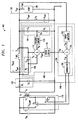
- the power converter 100 includes an inverter (power switching circuit) 110 coupled to an input of the power converter 100.
- the power converter 100 further includes a transformer T 1 having a primary winding S 1 coupled to the inverter 110 and a secondary winding S 2 .
- the power converter 100 further includes a rectifier 120, coupled to the secondary winding S 2 , that rectifies a periodic waveform supplied by the secondary winding S 2 .
- the power converter 100 further includes an output filter 130 coupled to the rectifier 120.
- the output filter 130 filters the rectified waveform from the rectifier 120 to supply an output voltage V OUT to a load 190 at an output of the power converter 100.
- the power converter 100 still further includes a control circuit 140, coupled to the inverter 110, that monitors the output voltage V OUT and adjusts the switching cycle of inverter 110 to regulate the output voltage V OUT . While the illustrated embodiment includes a transformer T 1 , those skilled in the pertinent art will realize that the transformer T 1 is not necessary to the present invention and that the principles of the present invention are applicable to isolated and non-isolated power converter topologies.
- the inverter 110 includes a power switch Q 1 coupled to the input of the power converter 100.
- the control circuit 140 intermittently switches the power switch Q 1 to impress a DC input voltage V IN across the primary winding S 1 .
- the inverter 110 includes a clamping circuit (having a clamping switch Q 2 and a clamping capacitor C CLAMP ) to reset the flux in the transformer T 1 during the off period of the power switch Q 1 . While the embodiment illustrated and described shows a generic inverter 110, those skilled in the art will realize that the principles of the present invention may be employed with a wide variety of inverter topologies.
- the rectifier 120 includes first and second rectifier diodes D 1 , D 2 arranged in a forward topology.
- first and second rectifier diodes D 1 , D 2 arranged in a forward topology.
- Those skilled in the art are familiar with forward rectifier circuits.
- other rectifier topologies, including those employing synchronous rectifiers, are well within the broad scope of the present invention.
- the output filter 130 includes an output capacitor C OUT , having an equivalent series resistance R esrC , coupled across the output of the power converter 100.
- the output filter 130 further includes a component coupled to the output capacitor C OUT .
- the component is an output inductor L OUT having an equivalent series resistance R esrL .
- control circuit 140 includes a feedback circuit 150.
- the feedback circuit 150 monitors the output voltage V OUT and adjusts the switching cycle of the inverter 110 to maintain the output voltage V OUT at a substantially constant level.
- the feedback circuit 150 includes an error amplifier 152 coupled to the output of the power converter 100.
- the error amplifier 152 monitors the output voltage V OUT and produces therefrom an error amplifier voltage V EA representing a difference between the output voltage V OUT and a reference voltage.
- the reference voltage may include a signal representing an output current I OUT or another parameter in the power converter 100.
- the feedback circuit 150 further includes a feedback summer circuit 154 coupled to the error amplifier 152 and a feedforward circuit 160.
- the feedback summer circuit 154 develops a threshold voltage V TH that is a sum of the error amplifier voltage V EA and a feedforward signal V FF from the feedforward circuit 160.
- the feedback circuit 150 still further includes a modulator 156 coupled to the feedback summer circuit 154.
- the modulator 156 compares the threshold voltage V TH to a periodic ramp signal and develops therefrom a switching waveform that drives the power switch Q 1 .
- the feedback circuit 150 may not be able to adequately regulate the output voltage V OUT when the power converter 100 is employed to power loads requiring wide bandwidth step changes in the output current.
- the control circuit 140 further includes the feedforward circuit 160 that estimates a time-varying output current I OUT to the load 190.
- the feedforward circuit 160 includes an observer circuit 164 parallel-coupled to the output capacitor C OUT (and its equivalent series resistance R esrC ).
- the observer circuit 164 is designed to indirectly measure a capacitor current I C through the output capacitor C OUT .
- the observer circuit 164 includes a series-coupled capacitor C 1 and resistor R 1 .
- a capacitor signal V IC representing the capacitor current I C may, therefore, be determined by measuring a resistor voltage V R1 across the resistor R 1 . While the illustrated observer circuit 164 employs a series-coupled capacitor and resistor, those skilled in the art realize that other observer circuits 164 are well within the broad scope of the present invention.
- the feedforward circuit 160 further includes a sensor circuit 168 coupled to the output inductor L OUT .
- the sensor circuit 168 is an observer circuit that indirectly measures an inductor current I L through the output inductor L OUT .
- the sensor circuit 168 need not be an observer circuit.
- the sensor circuit 168 includes a series-coupled capacitor C 2 and resistor R 2 .
- the sensor circuit 168 senses an inductor voltage V LOUT across the output inductor L OUT and develops therefrom an inductor signal V IL (component signal) representing the inductor current I L through the output inductor L OUT . While the illustrated sensor circuit 168 employs a series-coupled capacitor C 2 and resistor R 2 , those skilled in the art realize that other sensor circuits 168 are well within the broad scope of the present invention.
- the feedforward circuit 160 further includes a feedforward summer circuit 172 coupled to the observer circuit 164 and the sensor circuit 168.
- the feedforward circuit 160 further includes a scaling circuit 174 coupled between the observer circuit 164 and the feedforward summer circuit 172.
- the scaling circuit 174 adjusts a gain of the capacitor signal V IC relative to the inductor signal V IL .
- the scaling circuit 174 may be coupled between the sensor circuit 168 and the feedforward summer circuit 172 to adjust a gain of the inductor signal V IL relative to capacitor signal V IC .
- the scaling circuit 174 is not required to practice the present invention.
- the scaling circuit 174 advantageously adjusts a scaling factor measured in amperes/volt of the capacitor signal V IC or the inductor signal V IL to enable the feedforward summer circuit 172 to derive an output signal V IOUT representing the output current I OUT of the power converter 100.
- Those skilled in the art are familiar with scaling circuits.
- the feedforward circuit 160 still further includes a filter circuit 176 coupled to the feedforward summer circuit 172.
- the filter circuit 176 receives the output signal V IOUT from the feedforward summer circuit 172 and develops therefrom the feedforward signal V FF .
- the filter circuit 176 frequency shapes the output signal V IOUT to produce the feedforward signal V FF .
- the filter circuit 176 may adjust a gain of the output signal V IOUT as required to allow the feedback circuit 150 to properly employ the feedforward signal V FF .
- Those skilled in the art are familiar with the frequency shaping capability of filter circuits.
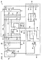
- FIGURE 2 illustrated is a schematic diagram of another embodiment of a power converter 200 constructed in accordance with the principles of the present invention.
- the power converter 200 includes an inverter 210, having a power switch Q1, coupled to an input of the power converter 200. While the inverter 210 is illustrated as a generic inverter, those skilled in the art will realize that the principles of the present invention may be employed with a wide variety of inverter topologies.
- the power converter 200 further includes a transformer T 1 having primary winding S 1 coupled to the inverter 210 and a secondary winding S 2 .
- the power converter 200 further includes a rectifier 220, coupled to the secondary winding S 2 , that rectifies a periodic waveform supplied by the secondary winding S 2 . While the power converter 200 employs a forward rectifier 220, other rectifier topologies are well within the broad scope of the present invention.
- the power converter 200 further includes an output filter 230, coupled to the rectifier 220, that filters the rectified waveform from the rectifier 220 to supply an output voltage V OUT to a load 290 at an output of the power converter 200.
- the output filter 230 includes an output capacitor C OUT , having an equivalent series resistance R esrC , coupled across the output of the power converter 200.
- the output filter 230 further includes an output inductor L OUT , having an equivalent series resistance R esrL , coupled to the output capacitor C OUT .
- the equivalent series resistances R esrC , R esrL are intrinsic to the output capacitor C OUT and the output inductor L OUT , respectively.
- the power converter 200 still further includes a control circuit 240 coupled to the inverter 210.
- the control circuit 240 includes a feedback circuit 250 and a feedforward circuit 270.
- the feedforward circuit 270 estimates a time-varying output current I OUT to the load 190 and develops therefrom a feedforward signal V FF .
- the feedback circuit 250 monitors the output voltage V OUT and the feedforward signal V FF and adjusts the switching cycle of the inverter 210 to maintain the output voltage V OUT at a substantially constant level.
- the feedback circuit 250 includes a voltage scaling circuit 252, an error amplifier 255, a feedback summer circuit 260 and a modulator 265.
- the voltage scaling circuit 252 is coupled to the output of the power converter 200 and includes first and second voltage scaling resistors 253, 254.
- the voltage scaling circuit 252 scales the output voltage V OUT to develop a scaled output voltage.
- the error amplifier 255 is coupled to the voltage scaling circuit 252 and receives the scaled output voltage therefrom.
- the error amplifier 255 (and its associated compensation network) compares the scaled output voltage to a reference voltage V REF1 and develops therefrom an error amplifier voltage V EA representing a scaled difference between a desired output voltage (represented by the reference voltage V REF1 ) and the actual output voltage V OUT .
- the feedback summer circuit 260 is coupled to the error amplifier 255 and the feedforward circuit 270.
- the feedback summer circuit 260 receives the error amplifier voltage V EA and the feedforward signal V FF and develops therefrom a threshold signal V TH .
- the modulator 265 is coupled to the feedback summer circuit 260 and receives the threshold signal V TH therefrom.
- the modulator 265 compares the threshold voltage V TH to a periodic ramp signal V RAMP and develops therefrom a switching waveform that drives the power switch Q 1 .
- the feedforward circuit 270 includes an observer circuit 272, a sensor circuit 274, a feedforward summer circuit 280 and a filter circuit 285.
- the observer circuit 272 is parallel-coupled to the output capacitor C OUT and its equivalent series resistance R esrC to indirectly measure a capacitor current I C through the output capacitor C OUT .
- the observer circuit 272 includes a series-coupled capacitor C 1 and resistor R 1 .
- a capacitor signal representing the capacitor current I C may, therefore, be determined by measuring a resistor voltage across the resistor R 1 . While the illustrated observer circuit 272 employs a series-coupled capacitor and resistor, those skilled in the art realize that other observer circuits 272 are well within the broad scope of the present invention.
- the sensor circuit 274 is coupled to the output inductor L OUT and its equivalent series resistance R esrL .
- the sensor circuit 274 is an observer circuit that indirectly measures an inductor current I L through the output inductor L OUT .
- the sensor circuit 274 includes a series-coupled capacitor C 2 and resistor R 2 .
- the sensor circuit 274 senses a voltage across the output inductor L OUT and develops therefrom a component signal representing the inductor current I L . While the illustrated sensor circuit 274 employs a series-coupled capacitor C 2 and resistor R 2 , those skilled in the art realize that other sensor circuits 274 are well within the broad scope of the present invention.
- the feedforward summer circuit 280 is coupled to the observer circuit 272 and the sensor circuit 274.
- the feedforward summer circuit 280 includes a differential amplifier 282 and its associated circuitry. By selecting the components of the feedforward summer circuit 280, a scaled and weighted difference between the capacitor signal and the component signal may be obtained. The feedforward summer circuit 280 may thus derive an output signal representing the estimated output current I OUT of the power converter 100.
- the feedforward summer circuit 280 further includes a blocking capacitor C BLOCK coupled between the sensor circuit 274 and the differential amplifier 282. The blocking capacitor C BLOCK blocks a DC component of the output voltage V OUT from the differential amplifier 282.
- the filter circuit 285 is coupled between the feedforward summer circuit 280 and the feedback summer circuit 260 of the feedback circuit 250.
- the filter circuit 285 includes a capacitor 286 and a resistor 287 parallel-coupled across the capacitor 286.
- the resistor 287 adds a feedforward component to the feedback summer circuit 260 to compensate for parasitic resistances in an output path of the power converter 200.
- FIGURE 3A illustrates a first observer circuit 300.
- the first observer circuit 300 is parallel-coupled across the output capacitor C OUT (and its equivalent series resistance R esrC ) and includes a series-coupled capacitor C 1 and resistor R 1 .
- the first observer circuit 300 is designed to observe a capacitor current I C through the output capacitor C OUT .
- a resistor voltage V R1 across the resistor R 1 may be represented by the following equation.
- V R 1 I C ⁇ R 1 ⁇ C 1 C OUT 1+ s ⁇ R esrC ⁇ C out 1+ s ⁇ R 1 ⁇ C 1
- the above equation may be simplified by selecting the capacitor C 1 and the resistor R 1 such that a time constant thereof is equivalent to a time constant of the output capacitor C OUT and its equivalent series resistance R esrC .
- the capacitor current I C through the output capacitor C OUT may thus be represented as set forth below.
- I C V R 1 ⁇ C OUT R 1 ⁇ C 1
- the capacitor current I C may, therefore, be determined by measuring the resistor voltage V R1 .
- FIGURE 3B illustrated is a second observer circuit 350 constructed in accordance with the principles of the present invention.
- the second observer circuit 350 is also parallel-coupled across the output capacitor C OUT and may be employed to observe the capacitor current I C through the output capacitor C OUT .
- the second observer circuit 350 includes a series-coupled resistor R 2 and inductor L 2 .
- the capacitor current I C is related to an inductor voltage V L2 across the inductor L 2 by the following equation.
- the inductor L 2 and the resistor R 2 are selected such that a time constant thereof is equivalent to a time constant of the output capacitor C OUT and its equivalent series resistance R esrC , the above equation may be simplified as set forth below.
- I C V L 2 R esrC
- the capacitor current I C may, therefore, be determined by measuring the inductor voltage V L2 .
- FIGURE 4A illustrates a first sensor circuit 400.
- the first sensor circuit 400 is an observer circuit that indirectly measures an inductor current I L through the output inductor L OUT .
- the first sensor circuit 400 is parallel-coupled across the output inductor L OUT (and its equivalent series resistance R esrL ) and includes a series-coupled resistor R 1 and capacitor C 1 .
- the inductor current I L develops a capacitor voltage V C1 across the capacitor C 1 .
- the capacitor voltage V C1 may be represented by the following equation.
- the above equation may be simplified by selecting the resistor R 1 and the capacitor C 1 such that a time constant thereof is equivalent to a time constant of the output inductor L OUT and its equivalent series resistance R esrL .
- the inductor current I L through the output inductor L OUT may thus be represented as set forth below.
- I L V C 1 R esrL
- the inductor current I L may, therefore, be determined by measuring the capacitor voltage V C1 .
- FIGURE 4B illustrated is a second sensor circuit 450 constructed in accordance with the principles of the present invention.
- the second sensor circuit 450 is an observer circuit that indirectly measures the inductor current I L through the output inductor L OUT .
- the second sensor circuit 450 is parallel-coupled across the output inductor L OUT and includes a series-coupled resistor R 2 and inductor L 2 .
- the inductor current I L is related to a resistor voltage V R2 across the resistor R 2 by the following equation.
- the inductor L 2 and the resistor R 2 are selected such that a time constant thereof is equivalent to a time constant of the output inductor L OUT and its equivalent series resistance R esrL , the above equation may be simplified as set forth below.
- I L V R 2 R esrL
- the inductor current I L may, therefore, be determined by measuring the resistor voltage V R2 .
- the first and second sensor circuits 400, 450 are submitted for illustrative purposes only and that other sensor circuits capable of measuring a characteristic of the component (e.g. , the inductor current I L through the output inductor L OUT ) are well within the broad scope of the present invention.
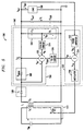
- FIGURE 5 illustrated is a schematic diagram of another embodiment of a power converter 500 constructed in accordance with the principles of the present invention.
- the power converter 500 employs a flyback topology and includes an inverter 510 coupled to an input of the power converter 500.
- the power converter 500 further includes a transformer T 1 having a primary winding S 1 coupled to the inverter 510 and a secondary winding S 2 .
- the inverter 510 switches intermittently to apply a DC input voltage V IN across the primary winding S 1 of the transformer T 1 .
- the power converter 500 further includes a rectifier 520 coupled to the secondary winding S 2 .
- the rectifier 520 includes a flyback diode D 1 that rectifies a periodic waveform supplied by the secondary winding S 2 .
- the power converter 500 further includes an output capacitor C OUT coupled to the flyback diode D 1 .
- the output capacitor C OUT filters the rectified waveform from the rectifier 520 to supply an output voltage V OUT to a load 590 at an output of the power converter 500.
- the equivalent series resistance R esrC of the output capacitor C OUT is explicitly illustrated. Those skilled in the art realize, of course, that the equivalent series resistance R esrC is intrinsic to the output capacitor C OUT .
- the power converter 500 still further includes a control circuit 540 coupled to the inverter 510.
- control circuit 540 includes a feedback circuit 550 that monitors the output voltage V OUT and adjusts the switching cycle of inverter 510 to regulate the output voltage V OUT .
- the control circuit 540 further includes a feedforward circuit 560 that estimates a time-varying output current I OUT to the load 590.
- the feedback circuit 550 includes an error amplifier 552 coupled to the output of the power converter 500.
- the error amplifier 552 monitors the output voltage V OUT and produces therefrom an error amplifier voltage V EA representing a difference between the output voltage V OUT and a reference voltage.
- the reference voltage may include a signal representing the output current I OUT or another parameter in the power converter 500.
- the feedback circuit 550 thither includes a feedback summer circuit 554 coupled to the error amplifier 552 and the feedforward circuit 560.
- the feedback summer circuit 554 develops a threshold voltage V TH that is a sum of the error amplifier voltage V EA and a feedforward signal V FF from the feedforward circuit 560.
- the feedback circuit 550 still further includes a modulator 556 coupled to the feedback summer circuit 554.
- the modulator 556 compares the threshold voltage V TH to a periodic ramp signal and develops therefrom a switching waveform that drives the power switch Q 1 .
- the feedforward circuit 560 includes an observer circuit 564, parallel-coupled to the output capacitor C OUT (and its equivalent series resistance R esrC ), that indirectly measures a capacitor current I C through the output capacitor C OUT .
- the observer circuit 564 includes a series-coupled capacitor C 1 and resistor R 1 .
- a capacitor signal V IC representing the capacitor current I C may, therefore, be developed by measuring a resistor voltage V R1 across the resistor R 1 . While the illustrated observer circuit 564 employs a series-coupled capacitor and resistor, those skilled in the art realize that other observer circuits are well within the broad scope of the present invention.
- the feedforward circuit 560 further includes a sensor circuit 568 series-coupled to the flyback diode D 1 .
- the sensor circuit 568 includes a sense resistor R SENSE .
- the sensor circuit 568 may include other elements, such as a current-sensing transformer. In either case, the sensor circuit 568 directly measures the voltage across the sense resistor R SENSE and develops a flyback signal V ID (component signal) representing the current through the flyback diode D 1 .
- the feedforward circuit 560 further includes a feedforward summer circuit 572 coupled to the observer circuit 564 and the sensor circuit 568.
- the feedforward circuit 560 further includes a scaling circuit 574 coupled between the observer circuit 564 and the feedforward summer circuit 572.
- the scaling circuit 560 adjusts a gain of the capacitor signal V IC relative to the flyback signal V ID .
- the scaling circuit 574 may be coupled between the sensor circuit 568 and the feedforward summer circuit 572 to adjust a gain of the flyback signal V ID relative to capacitor signal V IC .
- the scaling circuit 574 is not required to practice the present invention.
- the scaling circuit 574 advantageously adjusts a scaling factor measured in amperes/volt of the capacitor signal V IC or the flyback signal V ID to enable the feedforward summer circuit 572 to derive an output signal V IOUT representing the output current I OUT of the power converter 500.
- Those skilled in the art are familiar with scaling circuits.
- the feedforward circuit 560 still further includes a filter circuit 576 coupled to the feedforward summer circuit 572.
- the filter circuit 576 receives the output signal V IOUT from the feedforward summer circuit 572 and develops therefrom the feedforward signal V FF .
- the filter circuit 576 frequency shapes the output signal V IOUT to produce the feedforward signal V FF .
- the filter circuit 576 may adjust a gain of the output signal V IOUT as required to allow the feedback circuit 550 to properly employ the feedforward signal V FF .
- Those skilled in the art are familiar with the frequency shaping capability of filter circuits.
- the observer and sensor circuits 564, 568 thus cooperate to provide the feedforward circuit 560 with a measurement of the output current I OUT .
- the feedforward signal V FF may, therefore, be supplied to the feedback circuit 550 to allow the control circuit 540 to compensate for the fast changes in the output current I OUT required by the load 590.
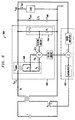
- FIGURE 6 illustrated is a schematic diagram of yet another embodiment of a power converter 600 constructed in accordance with the principles of the present invention.
- the power converter 600 is substantially similar to the power converter 500 of FIGURE 5 and, as a result, will not be described in detail.
- the power converter 600 includes a feedforward circuit 660 having an observer circuit 664 and a sensor circuit 668.
- the observer circuit 664 is parallel-coupled across the output capacitor C OUT while the sensor circuit 668 is series-coupled to the flyback diode D 1 .
- the sensor circuit 668 includes a current-sensing transformer T SENSE .
- the sensor circuit 668 further includes a resistor R S coupled across the current-sensing transformer T SENSE .
- the sensor circuit 668 still further includes a diode D S coupled between a terminal of the current-sensing transformer T SENSE and the feedforward summer circuit 672.
- the sensor circuit 668 develops a voltage signal V ID (component signal) across the resistor R S that is proportional to the current I D1 through the flyback diode D 1 .
- V ID component signal
- Those skilled in the art are familiar with current-sensing transformers and their operation. Of course, the use of other components may be coupled in series with the flyback diode D 1 and be well within the broad scope of the present invention.
- the principles of the present invention may be applied to various other converter topologies such as half bridge, full bridge, flyback, and boost converter topologies employing discrete or integrated magnetics.
- converter topologies employing discrete and integrated magnetic techniques, see Modern DC-to-DC Switchmode Power Converter Circuits , by Rudolph P. Severns and Gordon Bloom, Van Nostrand Reinhold Company, New York, New York (1985) and Principles of Solid-State Power conversion, by Ralph E. Tarter, Howard W. Sam & Co., Inc., Indianapolis, Indiana (1985), which are incorporated herein by reference in their entirety.
Landscapes
- Physics & Mathematics (AREA)
- General Physics & Mathematics (AREA)
- Engineering & Computer Science (AREA)
- Power Engineering (AREA)
- Dc-Dc Converters (AREA)
- Measurement Of Current Or Voltage (AREA)
- Control Of Voltage And Current In General (AREA)
Applications Claiming Priority (2)
| Application Number | Priority Date | Filing Date | Title |
|---|---|---|---|
| US374217 | 1989-06-29 | ||
| US09/374,217 US6249447B1 (en) | 1999-08-13 | 1999-08-13 | System and method for determining output current and converter employing the same |
Publications (1)
| Publication Number | Publication Date |
|---|---|
| EP1087509A2 true EP1087509A2 (de) | 2001-03-28 |
Family
ID=23475843
Family Applications (1)
| Application Number | Title | Priority Date | Filing Date |
|---|---|---|---|
| EP00306516A Withdrawn EP1087509A2 (de) | 1999-08-13 | 2000-07-31 | Verfahren und Vorrichtung zur Ausgangsstrombestimmung und Umrichter der diese anwendet |
Country Status (3)
| Country | Link |
|---|---|
| US (1) | US6249447B1 (de) |
| EP (1) | EP1087509A2 (de) |
| JP (1) | JP2001100849A (de) |
Cited By (5)
| Publication number | Priority date | Publication date | Assignee | Title |
|---|---|---|---|---|
| EP1085647A3 (de) * | 1999-09-15 | 2003-04-16 | Lucent Technologies Inc. | Kompensationsschaltung, Verfahren zum Betrieb derselben und Umrichter der diese anwendet |
| EP2113996A3 (de) * | 2001-09-25 | 2010-01-06 | Daikin Industries, Ltd. | Phasenstromerkennungsvorrichtung |
| WO2012075229A3 (en) * | 2010-12-03 | 2012-12-06 | Microchip Technology Incorporated | Lossless inductor current sensing in a switch-mode power supply |
| WO2013090112A3 (en) * | 2011-12-15 | 2013-08-15 | Eaton Corporation | System and method for detecting phase loss and diagnosing dc link capacitor health in an adjustable speed drive |
| CN105866582A (zh) * | 2016-04-15 | 2016-08-17 | 孝感致诚科技服务有限公司 | 一种电子镇流器的检测装置及方法 |
Families Citing this family (97)
| Publication number | Priority date | Publication date | Assignee | Title |
|---|---|---|---|---|
| US6724220B1 (en) | 2000-10-26 | 2004-04-20 | Cyress Semiconductor Corporation | Programmable microcontroller architecture (mixed analog/digital) |
| US8103496B1 (en) | 2000-10-26 | 2012-01-24 | Cypress Semicondutor Corporation | Breakpoint control in an in-circuit emulation system |
| US7765095B1 (en) | 2000-10-26 | 2010-07-27 | Cypress Semiconductor Corporation | Conditional branching in an in-circuit emulation system |
| US8176296B2 (en) | 2000-10-26 | 2012-05-08 | Cypress Semiconductor Corporation | Programmable microcontroller architecture |
| US8149048B1 (en) | 2000-10-26 | 2012-04-03 | Cypress Semiconductor Corporation | Apparatus and method for programmable power management in a programmable analog circuit block |
| US8160864B1 (en) | 2000-10-26 | 2012-04-17 | Cypress Semiconductor Corporation | In-circuit emulator and pod synchronized boot |
| US7042952B1 (en) * | 2001-02-12 | 2006-05-09 | Custom One Design, Inc. | Methods and apparatuses for receiving and transmitting signals |
| US6449177B1 (en) * | 2001-08-14 | 2002-09-10 | Lee-Fei Chen | Power supply having a mixed mode regulator |
| US7406674B1 (en) | 2001-10-24 | 2008-07-29 | Cypress Semiconductor Corporation | Method and apparatus for generating microcontroller configuration information |
| US8078970B1 (en) | 2001-11-09 | 2011-12-13 | Cypress Semiconductor Corporation | Graphical user interface with user-selectable list-box |
| US8042093B1 (en) | 2001-11-15 | 2011-10-18 | Cypress Semiconductor Corporation | System providing automatic source code generation for personalization and parameterization of user modules |
| US8069405B1 (en) | 2001-11-19 | 2011-11-29 | Cypress Semiconductor Corporation | User interface for efficiently browsing an electronic document using data-driven tabs |
| US6971004B1 (en) | 2001-11-19 | 2005-11-29 | Cypress Semiconductor Corp. | System and method of dynamically reconfiguring a programmable integrated circuit |
| US7844437B1 (en) | 2001-11-19 | 2010-11-30 | Cypress Semiconductor Corporation | System and method for performing next placements and pruning of disallowed placements for programming an integrated circuit |
| US7770113B1 (en) | 2001-11-19 | 2010-08-03 | Cypress Semiconductor Corporation | System and method for dynamically generating a configuration datasheet |
| US7774190B1 (en) | 2001-11-19 | 2010-08-10 | Cypress Semiconductor Corporation | Sleep and stall in an in-circuit emulation system |
| US8103497B1 (en) | 2002-03-28 | 2012-01-24 | Cypress Semiconductor Corporation | External interface for event architecture |
| US7308608B1 (en) | 2002-05-01 | 2007-12-11 | Cypress Semiconductor Corporation | Reconfigurable testing system and method |
| US7761845B1 (en) | 2002-09-09 | 2010-07-20 | Cypress Semiconductor Corporation | Method for parameterizing a user module |
| US20040125621A1 (en) * | 2002-12-30 | 2004-07-01 | Ta-Yung Yang | Synchronous rectifier of flyback power converter |
| US7295049B1 (en) | 2004-03-25 | 2007-11-13 | Cypress Semiconductor Corporation | Method and circuit for rapid alignment of signals |
| US8069436B2 (en) | 2004-08-13 | 2011-11-29 | Cypress Semiconductor Corporation | Providing hardware independence to automate code generation of processing device firmware |
| US8286125B2 (en) | 2004-08-13 | 2012-10-09 | Cypress Semiconductor Corporation | Model for a hardware device-independent method of defining embedded firmware for programmable systems |
| US7332976B1 (en) | 2005-02-04 | 2008-02-19 | Cypress Semiconductor Corporation | Poly-phase frequency synthesis oscillator |
| US7400183B1 (en) | 2005-05-05 | 2008-07-15 | Cypress Semiconductor Corporation | Voltage controlled oscillator delay cell and method |
| US8089461B2 (en) | 2005-06-23 | 2012-01-03 | Cypress Semiconductor Corporation | Touch wake for electronic devices |
| US8159203B2 (en) | 2005-08-01 | 2012-04-17 | St-Ericsson Sa | DC-DC converter with switchable estimators |
| US7307485B1 (en) | 2005-11-14 | 2007-12-11 | Cypress Semiconductor Corporation | Capacitance sensor using relaxation oscillators |
| US8085067B1 (en) | 2005-12-21 | 2011-12-27 | Cypress Semiconductor Corporation | Differential-to-single ended signal converter circuit and method |
| US7312616B2 (en) | 2006-01-20 | 2007-12-25 | Cypress Semiconductor Corporation | Successive approximate capacitance measurement circuit |
| US20070176903A1 (en) * | 2006-01-31 | 2007-08-02 | Dahlin Jeffrey J | Capacitive touch sensor button activation |
| US8067948B2 (en) | 2006-03-27 | 2011-11-29 | Cypress Semiconductor Corporation | Input/output multiplexer bus |
| US8144125B2 (en) | 2006-03-30 | 2012-03-27 | Cypress Semiconductor Corporation | Apparatus and method for reducing average scan rate to detect a conductive object on a sensing device |
| US7721609B2 (en) | 2006-03-31 | 2010-05-25 | Cypress Semiconductor Corporation | Method and apparatus for sensing the force with which a button is pressed |
| US8040142B1 (en) | 2006-03-31 | 2011-10-18 | Cypress Semiconductor Corporation | Touch detection techniques for capacitive touch sense systems |
| US7459893B2 (en) * | 2006-04-20 | 2008-12-02 | Mark E Jacobs | Optimal feedback control of switch-mode power converters |
| US8089472B2 (en) | 2006-05-26 | 2012-01-03 | Cypress Semiconductor Corporation | Bidirectional slider with delete function |
| US8537121B2 (en) | 2006-05-26 | 2013-09-17 | Cypress Semiconductor Corporation | Multi-function slider in touchpad |
| US8040321B2 (en) | 2006-07-10 | 2011-10-18 | Cypress Semiconductor Corporation | Touch-sensor with shared capacitive sensors |
| US7253643B1 (en) | 2006-07-19 | 2007-08-07 | Cypress Semiconductor Corporation | Uninterrupted radial capacitive sense interface |
| US9507465B2 (en) | 2006-07-25 | 2016-11-29 | Cypress Semiconductor Corporation | Technique for increasing the sensitivity of capacitive sensor arrays |
| KR100759897B1 (ko) * | 2006-08-02 | 2007-09-18 | 삼성전자주식회사 | 전류 검출 회로 및 방법 |
| US9766738B1 (en) | 2006-08-23 | 2017-09-19 | Cypress Semiconductor Corporation | Position and usage based prioritization for capacitance sense interface |
| US8547114B2 (en) * | 2006-11-14 | 2013-10-01 | Cypress Semiconductor Corporation | Capacitance to code converter with sigma-delta modulator |
| US8089288B1 (en) | 2006-11-16 | 2012-01-03 | Cypress Semiconductor Corporation | Charge accumulation capacitance sensor with linear transfer characteristic |
| US7642762B2 (en) * | 2007-01-29 | 2010-01-05 | Linear Technology Corporation | Current source with indirect load current signal extraction |
| US8058937B2 (en) | 2007-01-30 | 2011-11-15 | Cypress Semiconductor Corporation | Setting a discharge rate and a charge rate of a relaxation oscillator circuit |
| US9564902B2 (en) | 2007-04-17 | 2017-02-07 | Cypress Semiconductor Corporation | Dynamically configurable and re-configurable data path |
| US8092083B2 (en) | 2007-04-17 | 2012-01-10 | Cypress Semiconductor Corporation | Temperature sensor with digital bandgap |
| US8130025B2 (en) | 2007-04-17 | 2012-03-06 | Cypress Semiconductor Corporation | Numerical band gap |
| US7737724B2 (en) | 2007-04-17 | 2010-06-15 | Cypress Semiconductor Corporation | Universal digital block interconnection and channel routing |
| US8040266B2 (en) | 2007-04-17 | 2011-10-18 | Cypress Semiconductor Corporation | Programmable sigma-delta analog-to-digital converter |
| US8516025B2 (en) | 2007-04-17 | 2013-08-20 | Cypress Semiconductor Corporation | Clock driven dynamic datapath chaining |
| US8026739B2 (en) | 2007-04-17 | 2011-09-27 | Cypress Semiconductor Corporation | System level interconnect with programmable switching |
| US8065653B1 (en) | 2007-04-25 | 2011-11-22 | Cypress Semiconductor Corporation | Configuration of programmable IC design elements |
| US8266575B1 (en) | 2007-04-25 | 2012-09-11 | Cypress Semiconductor Corporation | Systems and methods for dynamically reconfiguring a programmable system on a chip |
| US9720805B1 (en) | 2007-04-25 | 2017-08-01 | Cypress Semiconductor Corporation | System and method for controlling a target device |
| US8144126B2 (en) | 2007-05-07 | 2012-03-27 | Cypress Semiconductor Corporation | Reducing sleep current in a capacitance sensing system |
| US9500686B1 (en) | 2007-06-29 | 2016-11-22 | Cypress Semiconductor Corporation | Capacitance measurement system and methods |
| US8089289B1 (en) | 2007-07-03 | 2012-01-03 | Cypress Semiconductor Corporation | Capacitive field sensor with sigma-delta modulator |
| US8169238B1 (en) | 2007-07-03 | 2012-05-01 | Cypress Semiconductor Corporation | Capacitance to frequency converter |
| WO2009006556A1 (en) | 2007-07-03 | 2009-01-08 | Cypress Semiconductor Corporation | Normalizing capacitive sensor array signals |
| US8570053B1 (en) | 2007-07-03 | 2013-10-29 | Cypress Semiconductor Corporation | Capacitive field sensor with sigma-delta modulator |
| US8049569B1 (en) | 2007-09-05 | 2011-11-01 | Cypress Semiconductor Corporation | Circuit and method for improving the accuracy of a crystal-less oscillator having dual-frequency modes |
| US8120346B2 (en) * | 2007-12-11 | 2012-02-21 | Infineon Technologies Austria Ag | Methods and apparatus for current sensing |
| US8044650B2 (en) * | 2007-12-11 | 2011-10-25 | Infineon Technologies Austria Ag | Methods and apparatus for current sensing in mutually coupled inductors |
| JP4768704B2 (ja) * | 2007-12-17 | 2011-09-07 | 富士通テレコムネットワークス株式会社 | 電流検出回路 |
| US8525798B2 (en) | 2008-01-28 | 2013-09-03 | Cypress Semiconductor Corporation | Touch sensing |
| US8487912B1 (en) | 2008-02-01 | 2013-07-16 | Cypress Semiconductor Corporation | Capacitive sense touch device with hysteresis threshold |
| US8319505B1 (en) | 2008-10-24 | 2012-11-27 | Cypress Semiconductor Corporation | Methods and circuits for measuring mutual and self capacitance |
| US8358142B2 (en) | 2008-02-27 | 2013-01-22 | Cypress Semiconductor Corporation | Methods and circuits for measuring mutual and self capacitance |
| US9104273B1 (en) | 2008-02-29 | 2015-08-11 | Cypress Semiconductor Corporation | Multi-touch sensing method |
| CN101572485B (zh) * | 2008-04-30 | 2012-06-06 | 杭州茂力半导体技术有限公司 | 用于副边同步整流管的智能驱动控制方法及装置 |
| US8321174B1 (en) | 2008-09-26 | 2012-11-27 | Cypress Semiconductor Corporation | System and method to measure capacitance of capacitive sensor array |
| US8487639B1 (en) | 2008-11-21 | 2013-07-16 | Cypress Semiconductor Corporation | Receive demodulator for capacitive sensing |
| DE112009004058T5 (de) * | 2008-11-21 | 2012-05-31 | L & L Engineering Llc | Verfahren und Systeme für die Komponentenwertschätzung inStromversorgungen/Leistungsumsetzern |
| CN102334076B (zh) * | 2008-11-21 | 2014-05-07 | L&L建筑公司 | 利用转移函数测量电源自适应控制的方法和系统 |
| US8866500B2 (en) | 2009-03-26 | 2014-10-21 | Cypress Semiconductor Corporation | Multi-functional capacitance sensing circuit with a current conveyor |
| US8358114B1 (en) * | 2009-04-28 | 2013-01-22 | Western Digital Technologies, Inc. | Output capacitor current as feedback to control a hysteretic voltage regulator |
| US9448964B2 (en) | 2009-05-04 | 2016-09-20 | Cypress Semiconductor Corporation | Autonomous control in a programmable system |
| US8749213B2 (en) * | 2009-06-09 | 2014-06-10 | Silergy Technology | Mixed mode control for switching regulator with fast transient responses |
| US8723827B2 (en) | 2009-07-28 | 2014-05-13 | Cypress Semiconductor Corporation | Predictive touch surface scanning |
| US8450988B2 (en) * | 2010-10-05 | 2013-05-28 | Maxim Integrated Products, Inc. | Systems and methods for controlling inductive energy in DC-DC converters |
| CN102609066A (zh) * | 2011-01-20 | 2012-07-25 | 鸿富锦精密工业(深圳)有限公司 | 多相电源供电电路 |
| JP2014506776A (ja) | 2011-02-11 | 2014-03-17 | バランセル(ピーティーワイ)リミテッド | 無損失インダクタ電流検出を行う双方向コンバータ用ヒステリシス電流モードコントローラ |
| US9268441B2 (en) | 2011-04-05 | 2016-02-23 | Parade Technologies, Ltd. | Active integrator for a capacitive sense array |
| CN102684490A (zh) * | 2012-04-28 | 2012-09-19 | 浙江大学 | 应用于单电感双输出降压变换器的定频准滑模控制器 |
| US8736244B1 (en) * | 2013-03-04 | 2014-05-27 | Google Inc. | Capacitive current-mode control of a DC/DC converter |
| FR3018967B1 (fr) * | 2014-03-21 | 2016-04-15 | Valeo Vision | Convertisseur asservi en courant de sortie |
| US20160268912A1 (en) * | 2015-03-12 | 2016-09-15 | Dell Products L.P. | Systems and methods for current sensing in a power system |
| US9733283B2 (en) * | 2015-04-23 | 2017-08-15 | Semiconductor Components Industries, Llc | DC-DC converter load current estimation circuit |
| US11099216B2 (en) * | 2016-03-03 | 2021-08-24 | Kongsberg Inc. | Circuit and method for shunt current sensing |
| US10224831B1 (en) * | 2018-01-22 | 2019-03-05 | Northern Power Systems, Inc. | Control systems, methods, and software for keeping power converters within operating limits during disturbances |
| EP3584902A1 (de) * | 2018-06-20 | 2019-12-25 | Siemens Gamesa Renewable Energy A/S | Dämpfung von schwingungen durch aktive filter |
| JP7361457B2 (ja) * | 2018-06-20 | 2023-10-16 | 新電元工業株式会社 | スイッチング電源装置 |
| US11460873B2 (en) * | 2020-06-09 | 2022-10-04 | Samsung Electronics Co., Ltd. | Power management integrated circuit including detection circuit with capacitive element |
| US12142998B2 (en) * | 2022-05-31 | 2024-11-12 | Texas Instruments Incorporated | System and method for estimating a current in an inductor of a power converter |
Family Cites Families (7)
| Publication number | Priority date | Publication date | Assignee | Title |
|---|---|---|---|---|
| US5481178A (en) * | 1993-03-23 | 1996-01-02 | Linear Technology Corporation | Control circuit and method for maintaining high efficiency over broad current ranges in a switching regulator circuit |
| US5747976A (en) * | 1996-03-26 | 1998-05-05 | Raytheon Company | Constant on-time architecture for switching regulators |
| US5757626A (en) * | 1996-06-21 | 1998-05-26 | Delta Electronics Inc. | Single-stage, single-switch, islolated power-supply technique with input-current shaping and fast output-voltage regulation |
| US5877611A (en) | 1996-10-09 | 1999-03-02 | Lucent Technologies Inc. | Simple and efficient switching regulator for fast transient loads such as microprocessors |
| US5991171A (en) * | 1998-02-05 | 1999-11-23 | Pi Electronics (H.K.) Ltd. | DC-to-DC converters |
| US5982160A (en) * | 1998-12-24 | 1999-11-09 | Harris Corporation | DC-to-DC converter with inductor current sensing and related methods |
| US6009000A (en) * | 1999-02-05 | 1999-12-28 | The Aerospace Corporation | Shared-bus current sharing parallel connected current-mode DC to DC converters |
-
1999
- 1999-08-13 US US09/374,217 patent/US6249447B1/en not_active Expired - Lifetime
-
2000
- 2000-07-31 EP EP00306516A patent/EP1087509A2/de not_active Withdrawn
- 2000-08-11 JP JP2000243503A patent/JP2001100849A/ja active Pending
Cited By (9)
| Publication number | Priority date | Publication date | Assignee | Title |
|---|---|---|---|---|
| EP1085647A3 (de) * | 1999-09-15 | 2003-04-16 | Lucent Technologies Inc. | Kompensationsschaltung, Verfahren zum Betrieb derselben und Umrichter der diese anwendet |
| EP2113996A3 (de) * | 2001-09-25 | 2010-01-06 | Daikin Industries, Ltd. | Phasenstromerkennungsvorrichtung |
| WO2012075229A3 (en) * | 2010-12-03 | 2012-12-06 | Microchip Technology Incorporated | Lossless inductor current sensing in a switch-mode power supply |
| US8447275B2 (en) | 2010-12-03 | 2013-05-21 | Microchip Technology Incorporated | Lossless inductor current sensing in a switch-mode power supply |
| WO2013090112A3 (en) * | 2011-12-15 | 2013-08-15 | Eaton Corporation | System and method for detecting phase loss and diagnosing dc link capacitor health in an adjustable speed drive |
| US8796982B2 (en) | 2011-12-15 | 2014-08-05 | Eaton Corporation | System and method for detecting phase loss and diagnosing DC link capacitor health in an adjustable speed drive |
| CN104040441A (zh) * | 2011-12-15 | 2014-09-10 | 伊顿公司 | 用于在可调节速度驱动器中检测相位损耗并且诊断dc链路电容器健康的系统和方法 |
| CN105866582A (zh) * | 2016-04-15 | 2016-08-17 | 孝感致诚科技服务有限公司 | 一种电子镇流器的检测装置及方法 |
| CN105866582B (zh) * | 2016-04-15 | 2019-02-22 | 孝感致诚科技服务有限公司 | 一种电子镇流器的检测装置及方法 |
Also Published As
| Publication number | Publication date |
|---|---|
| US6249447B1 (en) | 2001-06-19 |
| JP2001100849A (ja) | 2001-04-13 |
Similar Documents
| Publication | Publication Date | Title |
|---|---|---|
| US6249447B1 (en) | System and method for determining output current and converter employing the same | |
| US6828762B2 (en) | Inductor current sensing in isolated switching regulators and related methods | |
| CN101741244B (zh) | 提高功率因数校正电路中的效率的方法和装置 | |
| Erickson | DC–DC power converters | |
| EP0636889B1 (de) | Schaltnetzteil mit einer Schaltung zum Abschätzen des Ausgangsstroms | |
| KR101584169B1 (ko) | 스위칭 조정기 및 이를 이용한 전압을 조정하는 방법 | |
| US6069807A (en) | Compensation circuit method of operations thereof and converter employing the same | |
| US9391523B2 (en) | Controller with constant current limit | |
| US20130021008A1 (en) | Power converter apparatus and method with compensation for light load conditions | |
| US6396725B1 (en) | System and method for improving control loop response of a power supply | |
| US8964412B2 (en) | Split current mirror line sensing | |
| US12278551B2 (en) | Trans-inductor voltage regulator current sensing techniques | |
| US7352161B2 (en) | Burst-mode switching voltage regulator with ESR compensation | |
| Sheehan et al. | Switch-mode power converter compensation made easy | |
| US5917312A (en) | System and method for voltage positioning a regulator and regulator employing the same | |
| JP2868422B2 (ja) | 電力変換における電流検出装置及び方法 | |
| CN104283420A (zh) | 具压降补偿功能的电压转换控制器及电压转换电路 | |
| TWI867081B (zh) | 用於電力轉換器之電壓模式控制的數位非線性變換 | |
| US5629841A (en) | Low power dc-dc converter | |
| US20070069699A1 (en) | Dc/dc converter with inductor current sensing capability | |
| CA2746761A1 (en) | Power converter apparatus and methods | |
| JP3324096B2 (ja) | クロス・レギュレーション・チョークコイルを用いた多出力直流電源装置 | |
| JP3001057B1 (ja) | スイッチング電源装置及びその制御方法 | |
| Controller | Dual Synchronous | |
| Blanc | A 1-Watt Flyback Converter Using the Si9100 |
Legal Events
| Date | Code | Title | Description |
|---|---|---|---|
| PUAI | Public reference made under article 153(3) epc to a published international application that has entered the european phase |
Free format text: ORIGINAL CODE: 0009012 |
|
| AK | Designated contracting states |
Kind code of ref document: A2 Designated state(s): AT BE CH CY DE DK ES FI FR GB GR IE IT LI LU MC NL PT SE |
|
| AX | Request for extension of the european patent |
Free format text: AL;LT;LV;MK;RO;SI |
|
| STAA | Information on the status of an ep patent application or granted ep patent |
Free format text: STATUS: THE APPLICATION HAS BEEN WITHDRAWN |
|
| 18W | Application withdrawn |
Withdrawal date: 20020208 |