EP1089212A2 - Steckkarte für elektronische Geräte - Google Patents
Steckkarte für elektronische Geräte Download PDFInfo
- Publication number
- EP1089212A2 EP1089212A2 EP00118128A EP00118128A EP1089212A2 EP 1089212 A2 EP1089212 A2 EP 1089212A2 EP 00118128 A EP00118128 A EP 00118128A EP 00118128 A EP00118128 A EP 00118128A EP 1089212 A2 EP1089212 A2 EP 1089212A2
- Authority
- EP
- European Patent Office
- Prior art keywords
- plug
- card
- frame
- contacting device
- housing part
- Prior art date
- Legal status (The legal status is an assumption and is not a legal conclusion. Google has not performed a legal analysis and makes no representation as to the accuracy of the status listed.)
- Withdrawn
Links
Images


Classifications
-
- G—PHYSICS
- G06—COMPUTING OR CALCULATING; COUNTING
- G06K—GRAPHICAL DATA READING; PRESENTATION OF DATA; RECORD CARRIERS; HANDLING RECORD CARRIERS
- G06K7/00—Methods or arrangements for sensing record carriers, e.g. for reading patterns
- G06K7/04—Methods or arrangements for sensing record carriers, e.g. for reading patterns by mechanical means, e.g. by pins operating electric contacts
-
- H—ELECTRICITY
- H05—ELECTRIC TECHNIQUES NOT OTHERWISE PROVIDED FOR
- H05K—PRINTED CIRCUITS; CASINGS OR CONSTRUCTIONAL DETAILS OF ELECTRIC APPARATUS; MANUFACTURE OF ASSEMBLAGES OF ELECTRICAL COMPONENTS
- H05K5/00—Casings, cabinets or drawers for electric apparatus
- H05K5/02—Details
- H05K5/0256—Details of interchangeable modules or receptacles therefor, e.g. cartridge mechanisms
- H05K5/026—Details of interchangeable modules or receptacles therefor, e.g. cartridge mechanisms having standardized interfaces
- H05K5/0265—Details of interchangeable modules or receptacles therefor, e.g. cartridge mechanisms having standardized interfaces of PCMCIA type
- H05K5/0269—Card housings therefor, e.g. covers, frames, PCB
-
- G—PHYSICS
- G06—COMPUTING OR CALCULATING; COUNTING
- G06K—GRAPHICAL DATA READING; PRESENTATION OF DATA; RECORD CARRIERS; HANDLING RECORD CARRIERS
- G06K19/00—Record carriers for use with machines and with at least a part designed to carry digital markings
- G06K19/06—Record carriers for use with machines and with at least a part designed to carry digital markings characterised by the kind of the digital marking, e.g. shape, nature, code
- G06K19/067—Record carriers with conductive marks, printed circuits or semiconductor circuit elements, e.g. credit or identity cards also with resonating or responding marks without active components
- G06K19/07—Record carriers with conductive marks, printed circuits or semiconductor circuit elements, e.g. credit or identity cards also with resonating or responding marks without active components with integrated circuit chips
- G06K19/077—Constructional details, e.g. mounting of circuits in the carrier
-
- G—PHYSICS
- G06—COMPUTING OR CALCULATING; COUNTING
- G06K—GRAPHICAL DATA READING; PRESENTATION OF DATA; RECORD CARRIERS; HANDLING RECORD CARRIERS
- G06K19/00—Record carriers for use with machines and with at least a part designed to carry digital markings
- G06K19/06—Record carriers for use with machines and with at least a part designed to carry digital markings characterised by the kind of the digital marking, e.g. shape, nature, code
- G06K19/067—Record carriers with conductive marks, printed circuits or semiconductor circuit elements, e.g. credit or identity cards also with resonating or responding marks without active components
- G06K19/07—Record carriers with conductive marks, printed circuits or semiconductor circuit elements, e.g. credit or identity cards also with resonating or responding marks without active components with integrated circuit chips
- G06K19/077—Constructional details, e.g. mounting of circuits in the carrier
- G06K19/07737—Constructional details, e.g. mounting of circuits in the carrier the record carrier consisting of two or more mechanically separable parts
- G06K19/07741—Constructional details, e.g. mounting of circuits in the carrier the record carrier consisting of two or more mechanically separable parts comprising a first part operating as a regular record carrier and a second attachable part that changes the functional appearance of said record carrier, e.g. a contact-based smart card with an adapter part which, when attached to the contact card makes the contact card function as a non-contact card
Definitions
- the present invention relates to a plug-in card for electronic devices according to the preamble of Claim 1.
- Such plug-in cards are used for example as PC-cards according to the standards of the "Personal Computer Memory Card Industry Association” (PCMCIA) in portable computers (for example laptops, notebooks) in which the identification of the user for the use of, or access to, a service is required by means of a chip card, such as for example a SIM- or CCM-card.
- PCMCIA Personal Computer Memory Card Industry Association
- Such services can relate for example to credit cards, on-line services or the mobile telephone network.
- a plug-in card is known for example, wherein the chip card accommodating means is a separate component which can be inserted into the plug-in card and into the pivoted cover of which the chip card is plugged in (ITT Cannon Brochure "CCM-Plug Connector for Chip Cards 12/95").
- the structural height is problematic and on the other hand shielding problems arise in respect of the synthetic resin cover.
- the accommodating means is designed such that the chip card is inserted from the narrow side of the plug-in card.
- This type of chip card accommodating means on the narrow side of the plug-in card affects the stability of the plug-in card as an opening must be provided on the narrow side, which is substantially responsible for the rigidity. Therefore in most cases such an accommodating means requires a frameless plug-in card as otherwise the supporting frame must be interrupted.
- the object of the present invention is to provide a plug-in card for electronic devices of the type referred to in the introduction, the chip card accommodating means of which does not impair or negatively influence the structural height and stability of the plug-in card.
- the measures according to the invention provide that the chip card accommodating means can be used not only for frameless plug-in cards but also for those with a bracing frame without impairing the stability of the plug-in card. Due to the direct arrangement of the frame-like element on one of the housing parts, the required small structural height of the plug-in card is retained. As the frame is pre-mounted on the one housing part, a simplified assembly of the plug-in card is achieved.
- the frame-like element is secured on the underneath of the relevant housing part.
- the corresponding feature of Claim 3 is for example adhesively attached via a double-sided adhesive strip.
- the frame-like element can also be inserted into the opening in the relevant housing part and its edge portion can rest on the upper side of the housing part.
- the upper side of the relevant housing part can be provided with a small depression around the opening.
- the features according to Claim 7 are provided which facilitate a simple production of frame-like element and contacting device.
- the features according to Claim 8 are provided here.
- the contact arms of the contacting device which contact the relevant conductor paths of the circuit board, to be of sprung construction.
- the frame-like element and the contacting device are formed as separate components, such that the contacting device is attached to the circuit board and following the assembly of the plug-in card is accommodated in the recess of the frame-like component mounted on the housing part.
- the chip card can be readily removed from its use state, in which it is inserted in the plug-in card, by a finger-tip and thus by frictional engagement.
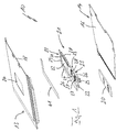
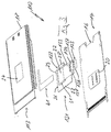
- the plug-in card 10, 110, 210 which is suitable for use in electronic devices, comprises an oblong and very flat frameless housing which is composed of a lower metallic housing part (not shown) and an upper metallic housing part 13, 113, 213 which is connectible or connected to said lower part by locking engagement at its longitudinal edge.
- a unit 14 is arranged and fixed between the lower housing part (not shown) and the upper housing part 13, 113, 213, which unit 14 comprises a circuit board 16 equipped with electronic components in a manner which has not been illustrated and, arranged at at least one transverse end of the circuit board 16, a plug-in connector (likewise not shown) connected thereto.
- the plug-in card 10, 110, 210 further comprises a device 21, 121, 221 for accommodating and holding a chip card 20, for example in the form of a SIM-, CCM- or the like card, as is used for plug-in cards, designed as PC cards according to the standards of the "Personal Computer Memory Card Industry Association (PCMCIA)", in portable computers, such as lap-tops, notebooks and the like.
- PCMCIA Personal Computer Memory Card Industry Association
- the device 21 according to the first exemplary embodiment of Figures 1 and 2 comprises a frame-like element 22 made of synthetic resin and a contact block or contacting device 23 which is electrically connectible to the circuit board 16.
- a rectangular opening 24 is provided through which the chip card 20 can be brought to the contacting device 23 via the frame-like element 22.
- the frame-like element 22 has a substantially approximately U-shaped frame 26 with legs of different length, of which the long leg 27 is wider than the parallel short leg 28.
- the two longitudinal legs 27 and 28 are connected by a transverse leg 29, the width of which corresponds approximately to that of the short longitudinal leg 28.
- the frame legs 27, 28 and 29 have a U-shaped, flange-like elevation 31, a ramp 32 extending in sloping fashion from the upper side of the transverse part of said elevation to the lower side thereof and continuing into a lower guide plate 33, the plane of which extends in parallel to the plane of the frame legs 27 to 29 and which projects beyond the long longitudinal leg 27.
- a mounting plate 36 of the contacting device 23 is arranged inside the guide plate 33.
- the contacts 37 of the contacting device 23 are inserted, and held stationery, in the mounting plate 36.
- the contacts 37 comprise first upper sprung ends 38, which project beyond the mounting plate 36 and which contact the chip card 20, and second, lower sprung ends 39 which in the assembled state contact the relevant conductor paths of the circuit board 16.
- the mounting plate 36 is thicker than the guide plate, their upper sides being aligned flush with one another.
- connection between the mounting plate 36 and the guide plate 33 is illustrated such that the mounting plate 36 is firmly inserted in a recess 34 of the guide plate 33 either by force-locking engagement or by an adhesive connection.
- the frame-like element 22 and the contacting device 23 form an integral component such that guide plate 33 and mounting plate 36 form one piece, the contacts 37 being injection-moulded into this one-piece plate 33, 36.
- the consequently integral component comprising frame-like element 22 and contacting device 23 is attached to the underneath 18 of the upper housing part 13 in such manner that the U-shaped elevation 31 of the frame 26 is arranged inside the opening 24 and bears against the inner edges thereof.
- an attachment in the form of an adhesion of housing part 13 and frame-like element 22 is employed.
- a L-shaped, double-sided adhesive strip 41 is used which, adjacent to the U-shaped elevation 31, is adhesively attached on the one hand to the long longitudinal leg 27 and the transverse leg 29, and on the other hand to the underneath 18 of the housing part 13 surrounding the opening 24 in parts.
- the device 21 prior to the full assembly of the plug-in card 10, the device 21 is pre-mounted on the upper housing part 13, and specifically in such a way that upon the full assembly of the plug-in card 10 a corresponding contacting is readily achieved between the second sprung ends 39 of the contacts 37 and the relevant conductor paths of the circuit board 16.
- the U-shaped elevation 31 of the frame 26 lies within the relevant boundary edges of the opening 24, the inside outer dimensions of the U-shaped elevation 31 corresponding exactly to the inside inner dimensions of the opening 24.
- the U-shaped elevation 31 serves to guide the chip card 20 which can be pushed via the ramp 32 towards the guide plate 33 and onto the contacting device 23 and the contact sprung ends 38 thereof.
- a corresponding end stop for the chip card 20 can be formed on the guide plate 33 or can be formed by one or more components on the circuit board 16.
- the distance of the contacting device 23 from the opening 24 or the rear boundary thereof in the insertion direction is however such that, as shown in Figure 2, in its inserted state the chip card 20 can be "gripped" at its surface, for example by frictional engagement with a finger-tip, and removed from the frame-like element 22 via the ramp 23.
- frame-like element 122 and contacting device 123 constitute two interconnected yet separate components.
- the guide plate 133 comprises a recess 134 which is open at its free end and into which the mounting plate 136 of the contacting device 123 is snugly held and secured.
- the permanent connection can take place by force-locking or shape-locking or adhesion.
- the device 121 corresponds to the device 21 according to Figures 1 and 2 and is pre-mounted on the upper housing part 113 in the same manner.
- the plug-in card 210 shown in Figure 4 differs from the plug-in card 110 shown in Figure 3 inasmuch as the frame-like element 222 and the contacting device 323 of the device 221 are not only formed separately from one another but are also mounted on different parts of the plug-in card 210.
- the frame-like element 222 is secured on the upper housing part 213, for example by an adhesive connection, while the contacting device 223 is secured on the circuit board 16 however.
- the downwardly projecting second contact ends (not shown here) are of pin-like formation so that they can be soldered in corresponding metallized bores of the circuit board 16 in a manner which has not been shown.
- the positioning of the contacting device 223 on the circuit board 16 is such that upon the assembly of the plug-in card 210, the mounting plate 236 of the contacting device 223 fits snugly into the recess 234 of the guide plate 233.
- the frame-like element 22, 122, 222 is attached to the underneath of the upper housing part 13, 113, 213, it will be obvious that the lower housing part (not shown here) can be used instead for this purpose.
- the frame-like element 22, 122, 222 is applied to the relevant housing part not from the underneath but from the upper side through the opening 24.
- the frame-like element is provided with a U-shaped collar which projects beyond the relevant inside dimension of the opening 24 and which, surrounding the opening 24 for example in a U-formation, rests and is supported on the upper side of the relevant housing part.
- the opening 24 it can be expedient to arrange the opening 24 in a depression which is formed in the relevant housing part and which accommodates the bearing collar.
- the L-shaped adhesive strip 41 provided for the adhesive connection can be rendered conductive for shielding purposes in a manner not shown here.
Landscapes
- Engineering & Computer Science (AREA)
- Microelectronics & Electronic Packaging (AREA)
- Physics & Mathematics (AREA)
- General Physics & Mathematics (AREA)
- Theoretical Computer Science (AREA)
- Computer Hardware Design (AREA)
- Artificial Intelligence (AREA)
- Computer Vision & Pattern Recognition (AREA)
- Coupling Device And Connection With Printed Circuit (AREA)
- Credit Cards Or The Like (AREA)
- Casings For Electric Apparatus (AREA)
Applications Claiming Priority (2)
| Application Number | Priority Date | Filing Date | Title |
|---|---|---|---|
| DE19947162 | 1999-10-01 | ||
| DE19947162A DE19947162C1 (de) | 1999-10-01 | 1999-10-01 | Steckkarte für elektronische Geräte |
Publications (2)
| Publication Number | Publication Date |
|---|---|
| EP1089212A2 true EP1089212A2 (de) | 2001-04-04 |
| EP1089212A3 EP1089212A3 (de) | 2001-11-14 |
Family
ID=7924041
Family Applications (1)
| Application Number | Title | Priority Date | Filing Date |
|---|---|---|---|
| EP00118128A Withdrawn EP1089212A3 (de) | 1999-10-01 | 2000-08-28 | Steckkarte für elektronische Geräte |
Country Status (6)
| Country | Link |
|---|---|
| US (1) | US6421246B1 (de) |
| EP (1) | EP1089212A3 (de) |
| JP (1) | JP2001134737A (de) |
| KR (1) | KR20010050660A (de) |
| DE (1) | DE19947162C1 (de) |
| TW (1) | TW563013B (de) |
Families Citing this family (25)
| Publication number | Priority date | Publication date | Assignee | Title |
|---|---|---|---|---|
| US7107378B1 (en) * | 2000-09-01 | 2006-09-12 | Sandisk Corporation | Cooperative interconnection and operation of a non-volatile memory card and an input-output card |
| US6783926B2 (en) * | 2001-09-15 | 2004-08-31 | Kenneth Reece | Circuit board IC card connector |
| DE20201237U1 (de) | 2002-01-28 | 2002-06-13 | SCM Microsystems GmbH, 85737 Ismaning | Chipkartenlesegerät |
| US7440774B2 (en) | 2002-04-08 | 2008-10-21 | Socket Mobile, Inc. | Wireless enabled memory module |
| US7367503B2 (en) | 2002-11-13 | 2008-05-06 | Sandisk Corporation | Universal non-volatile memory card used with various different standard cards containing a memory controller |
| US8037229B2 (en) * | 2002-11-21 | 2011-10-11 | Sandisk Technologies Inc. | Combination non-volatile memory and input-output card with direct memory access |
| US20050055479A1 (en) * | 2002-11-21 | 2005-03-10 | Aviad Zer | Multi-module circuit card with inter-module direct memory access |
| DE10256716A1 (de) * | 2002-12-04 | 2004-06-24 | Siemens Ag | Chipkartenaufnahme |
| DE10303740B4 (de) * | 2003-01-30 | 2006-09-14 | Infineon Technologies Flash Gmbh & Co. Kg | Sicherheitsspeicherkarte und Herstellungsverfahren |
| US7305535B2 (en) * | 2003-04-17 | 2007-12-04 | Sandisk Corporation | Memory cards including a standard security function |
| DE10321242B4 (de) | 2003-05-12 | 2008-04-10 | Siemens Ag | Kartenaufnahmevorrichtung |
| US7209995B2 (en) * | 2003-12-09 | 2007-04-24 | Sandisk Corporation | Efficient connection between modules of removable electronic circuit cards |
| DE102006021023A1 (de) * | 2006-04-28 | 2007-10-31 | Würth Elektronik Rot am See GmbH & Co. KG | Baugruppenaufbau |
| US7572152B2 (en) * | 2007-06-27 | 2009-08-11 | Sandisk Il Ltd. | Memory interface card with SIM functions |
| CN101394716B (zh) * | 2007-09-19 | 2011-11-16 | 深圳富泰宏精密工业有限公司 | 壳体组件及具有该壳体组件的便携式电子装置 |
| US8718541B2 (en) * | 2007-12-31 | 2014-05-06 | Intel Corporation | Techniques for optimal location and configuration of infrastructure relay nodes in wireless networks |
| CN101553100A (zh) * | 2008-03-31 | 2009-10-07 | 深圳富泰宏精密工业有限公司 | 芯片卡固持结构 |
| US8462514B2 (en) | 2008-04-25 | 2013-06-11 | Apple Inc. | Compact ejectable component assemblies in electronic devices |
| CN101753644A (zh) * | 2008-12-10 | 2010-06-23 | 深圳富泰宏精密工业有限公司 | 便携式电子装置 |
| TWM367443U (en) * | 2008-12-26 | 2009-10-21 | D & Amp C Technology Co Ltd | Electronic card for smart card to insert in |
| US8325486B2 (en) * | 2009-01-13 | 2012-12-04 | Dy 4 Systems Inc. | Tamper respondent module |
| US8654535B2 (en) * | 2012-03-08 | 2014-02-18 | Proconn Technology Co., Ltd. | Card holder |
| CN103579853A (zh) * | 2012-08-06 | 2014-02-12 | 深圳富泰宏精密工业有限公司 | 芯片卡固持装置及应用其的电子装置 |
| USD707682S1 (en) * | 2012-12-05 | 2014-06-24 | Logomotion, S.R.O. | Memory card |
| US9195929B2 (en) * | 2013-08-05 | 2015-11-24 | A-Men Technology Corporation | Chip card assembling structure and method thereof |
Family Cites Families (6)
| Publication number | Priority date | Publication date | Assignee | Title |
|---|---|---|---|---|
| DE4029576C2 (de) * | 1990-09-18 | 1994-12-01 | Amphenol Tuchel Elect | Kontaktiereinrichtung für Standard-Chipkarte und SIM-Karte |
| JP3439868B2 (ja) * | 1995-03-20 | 2003-08-25 | 富士通株式会社 | 携帯電話機 |
| FR2747847B1 (fr) * | 1996-04-18 | 1998-07-03 | Itt Composants Instr | Boitier de raccordement electronique, a un ordinateur individuel, equipe d'un connecteur pour une carte a puce |
| DE29607253U1 (de) * | 1996-04-22 | 1996-07-04 | Stocko Metallwarenfabriken Henkels & Sohn GmbH & Co, 42327 Wuppertal | Kombichipkartenleser |
| GB2327792B (en) * | 1997-07-25 | 2001-09-12 | Nokia Mobile Phones Ltd | A data card housing |
| DE19846366C2 (de) * | 1998-04-07 | 2000-07-27 | Itt Mfg Enterprises Inc | Steckkarte für elektronische Geräte |
-
1999
- 1999-10-01 DE DE19947162A patent/DE19947162C1/de not_active Expired - Fee Related
-
2000
- 2000-08-28 EP EP00118128A patent/EP1089212A3/de not_active Withdrawn
- 2000-09-18 US US09/664,980 patent/US6421246B1/en not_active Expired - Fee Related
- 2000-09-21 JP JP2000286252A patent/JP2001134737A/ja active Pending
- 2000-09-27 KR KR1020000056665A patent/KR20010050660A/ko not_active Withdrawn
- 2000-09-30 TW TW089120393A patent/TW563013B/zh active
Also Published As
| Publication number | Publication date |
|---|---|
| US6421246B1 (en) | 2002-07-16 |
| DE19947162C1 (de) | 2000-09-28 |
| TW563013B (en) | 2003-11-21 |
| JP2001134737A (ja) | 2001-05-18 |
| EP1089212A3 (de) | 2001-11-14 |
| KR20010050660A (ko) | 2001-06-15 |
Similar Documents
| Publication | Publication Date | Title |
|---|---|---|
| EP1089212A2 (de) | Steckkarte für elektronische Geräte | |
| US5877488A (en) | Combination chip card reader | |
| EP1070446B1 (de) | Steckbare karte für ein elektrisches gerät | |
| US6095868A (en) | Card reader connector having a separable cover | |
| KR100433725B1 (ko) | 플래시 메모리 카드용 커넥터와 그것을 이용한 접속 구조및 이 접속 구조를 이용한 전자 장치 | |
| KR100447683B1 (ko) | 접촉형스마트카드용전기커넥터 | |
| JP3726215B2 (ja) | チップカード装置用接触装置 | |
| US5739515A (en) | IC card reader/writer | |
| US6231360B1 (en) | Memory card adapter | |
| US6398572B1 (en) | SIM (subscriber identity module) card holder with separate end stop | |
| JPH0836622A (ja) | マイクロサーキットカードの読取り装置 | |
| KR960043357A (ko) | Sim 카드 커넥터 | |
| US6244902B1 (en) | Smart card reader for elevated placement relative to a printed circuit board | |
| US7350705B1 (en) | Compact robust smart card reader | |
| EP1181849B1 (de) | Steckkarte für elektronische geräte | |
| US6508673B2 (en) | Low cost smart card reader, extension style, with wiping contacts | |
| HK1035421A (en) | A plug-in card for electronic devices | |
| US6527189B2 (en) | Card reader connector with removable extension bracket | |
| US7372136B2 (en) | Chip card retaining mechanism | |
| KR100227243B1 (ko) | 아이씨 카드 | |
| KR20050055412A (ko) | 이종 메모리 카드 겸용 소켓 | |
| JP3629986B2 (ja) | Icカードの装填装置 | |
| GB2360117A (en) | A SIM card holding device | |
| TW200905993A (en) | Electrical card connector | |
| HK1034852B (en) | Insertable card for electronic equipment |
Legal Events
| Date | Code | Title | Description |
|---|---|---|---|
| PUAI | Public reference made under article 153(3) epc to a published international application that has entered the european phase |
Free format text: ORIGINAL CODE: 0009012 |
|
| AK | Designated contracting states |
Kind code of ref document: A2 Designated state(s): DE FR GB Kind code of ref document: A2 Designated state(s): AT BE CH CY DE DK ES FI FR GB GR IE IT LI LU MC NL PT SE |
|
| AX | Request for extension of the european patent |
Free format text: AL;LT;LV;MK;RO;SI |
|
| PUAL | Search report despatched |
Free format text: ORIGINAL CODE: 0009013 |
|
| AK | Designated contracting states |
Kind code of ref document: A3 Designated state(s): AT BE CH CY DE DK ES FI FR GB GR IE IT LI LU MC NL PT SE |
|
| AX | Request for extension of the european patent |
Free format text: AL;LT;LV;MK;RO;SI |
|
| 17P | Request for examination filed |
Effective date: 20020410 |
|
| AKX | Designation fees paid |
Free format text: DE FR GB |
|
| STAA | Information on the status of an ep patent application or granted ep patent |
Free format text: STATUS: THE APPLICATION IS DEEMED TO BE WITHDRAWN |
|
| 18D | Application deemed to be withdrawn |
Effective date: 20051215 |
|
| REG | Reference to a national code |
Ref country code: HK Ref legal event code: WD Ref document number: 1035421 Country of ref document: HK |